EP0426270A2 - Dispositif de mémoire à semi-conducteurs portable - Google Patents
Dispositif de mémoire à semi-conducteurs portable Download PDFInfo
- Publication number
- EP0426270A2 EP0426270A2 EP90304512A EP90304512A EP0426270A2 EP 0426270 A2 EP0426270 A2 EP 0426270A2 EP 90304512 A EP90304512 A EP 90304512A EP 90304512 A EP90304512 A EP 90304512A EP 0426270 A2 EP0426270 A2 EP 0426270A2
- Authority
- EP
- European Patent Office
- Prior art keywords
- bus
- circuit
- data
- control
- address bus
- Prior art date
- Legal status (The legal status is an assumption and is not a legal conclusion. Google has not performed a legal analysis and makes no representation as to the accuracy of the status listed.)
- Granted
Links
Images



Classifications
-
- G—PHYSICS
- G06—COMPUTING OR CALCULATING; COUNTING
- G06F—ELECTRIC DIGITAL DATA PROCESSING
- G06F11/00—Error detection; Error correction; Monitoring
- G06F11/22—Detection or location of defective computer hardware by testing during standby operation or during idle time, e.g. start-up testing
- G06F11/2205—Detection or location of defective computer hardware by testing during standby operation or during idle time, e.g. start-up testing using arrangements specific to the hardware being tested
- G06F11/2221—Detection or location of defective computer hardware by testing during standby operation or during idle time, e.g. start-up testing using arrangements specific to the hardware being tested to test input/output devices or peripheral units
-
- G—PHYSICS
- G11—INFORMATION STORAGE
- G11C—STATIC STORES
- G11C5/00—Details of stores covered by group G11C11/00
-
- G—PHYSICS
- G11—INFORMATION STORAGE
- G11C—STATIC STORES
- G11C5/00—Details of stores covered by group G11C11/00
- G11C5/14—Power supply arrangements, e.g. power down, chip selection or deselection, layout of wirings or power grids, or multiple supply levels
- G11C5/141—Battery and back-up supplies
-
- G—PHYSICS
- G11—INFORMATION STORAGE
- G11C—STATIC STORES
- G11C5/00—Details of stores covered by group G11C11/00
- G11C5/14—Power supply arrangements, e.g. power down, chip selection or deselection, layout of wirings or power grids, or multiple supply levels
- G11C5/143—Detection of memory cassette insertion or removal; Continuity checks of supply or ground lines; Detection of supply variations, interruptions or levels ; Switching between alternative supplies
Definitions
- the present invention relates to a portable semiconductor memory device, and particularly to a memory device which allows access to internal memory when connected to a terminal equipment through a connector.
- Fig. 7 shows the configuration of a circuit of a conventional portable semiconductor memory device.
- the memory device has as an internal memory a static RAM 1 to which a battery 4 is connected through an internal power line 8 for supplying a power voltage, a reverse charge preventing diode 6 and a current limiting resistance 5.
- a power input line 7 is connected to the internal power line 8 through a power control circuit 3 and to a connector 35.
- a buffer circuit 2 is connected to the internal power line 8, the RAM 1 and the connector 35 being connected to each other by an address bus 10, a control bus 11 and a data bus 12 through the buffer circuit 2.
- the power control circuit 3 and the buffer circuit 2 are connected to each other by a control line 9.
- reference numeral 33 denotes a pull-up resistance connected between the internal power line 8 and the control bus 11.
- the memory device having the above-mentioned configuration When the memory device having the above-mentioned configuration is used, it is mounted on terminal equipment (not shown) through the connector 35. If a power voltage of a value greater than a defined value is applied to the power input line 7, the power control circuit 3 causes the connection between the power input line 7 and the internal power line 8, as well as sending a high level control signal to the buffer circuit 2 over the control line 9. This operation causes the power voltage supplied to the RAM 1 and the buffer circuit 2 over the internal power line 8, and the high level control signal brings the buffer circuit 2 into an enable (operable) state. In other words, the terminal equipment can get access to the RAM 1, i.e, reading from or writing in the RAM 1, over the address bus 10, the control bus 11 and the data bus 12. During this operation, since the potential of the internal power line 8 is set to a value higher than the potential of the positive side of the battery 4, the current of the battery 4 is not consumed.
- the power control circuit 3 When access to the RAM 1 is completed, and when a given power voltage is not applied to the power input line 7, the power control circuit 3 detects that the voltage value of the power input line 7 is less than the defined value and cuts off the connection between the power input line 7 and the internal power line 8, as well as sending a low level control signal to the buffer circuit 2 over the control line 9. The control signal brings the buffer circuit 2 into a disable (non-operating) state wherein any access to the RAM 1 is prohibited.
- the present invention has been achieved with a view to resolving the above-mentioned problem, and it is an object of the present invention to provide a portable semiconductor memory device which is capable of preventing any malfunction causing trouble in the connection of a connector.
- a portable semiconductor memory device in accordance with the present invention comprises internal memory for storing data, an address bus, a control bus and a data bus which are connected to the internal memory, a connector for electrically connecting the address bus, the control bus and the data bus to terminal equipment, and a contact confirmation/control circuit which is connected to the address bus, the control bus and the data bus and in which known data is previously stored so as to output the known data to the data bus when a reading control signal is input from the terminal equipment over the control bus and when a given address is specified on the address bus.
- the contact confirmation/control circuit can be constructed by a full-address bus "L” coincidence circuit for detecting that all the bits of the address bus are in the "L” level, a full-address bus “H” coincidence circuit for detecting that all the bits of the address bus are in the "H” level, a first memory circuit for storing first known data and outputting it to the data bus by the AND output of the read control signal input from the terminal equipment and the detection signal from the full-address bus "L” coincidence circuit, and a second storage circuit for storing second known data and outputting it to the data bus by the AND output of the read control signal input from the terminal equipment and the detection signal from the full-address bus "H” coincidence circuit.
- the first storage circuit may be provided with a change means for changing the level of a given bit of the first known data when a write control signal is input from the terminal equipment over the control bus.
- a portable semiconductor memory device A has as an internal memory a static RAM 1 to which a battery 4 is connected through an internal power line 8 for supplying a power voltage, a reverse charge preventing diode 6 and a current limiting resistance 5.
- a power input line 7 is connected to the internal power line 8 through a power control circuit 3 and to a connector 35.
- a buffer circuit 2 is also connected to the internal power line 8, and the RAM 1 is connected to the connector 35 by an address bus 10, a control bus 11 and a data bus 12 through the buffer circuit 2.
- the power control circuit 3 is connected to the buffer circuit 2 by a control line 9.
- reference numeral 33 denotes a pull-up resistance which is connected between the internal power line 8 and the control bus 11.
- a contact confirmation/control circuit 15 is connected to the address bus 10, the control bus 11 and the data bus 12.
- each of the address bus 10 and the data bus 12 comprises a 8-bit bus
- the control bus 11 is formed by a write-enable signal line 13, a card-enable signal line 14 and an output-enable signal line 26.
- a test signal line 16 is also connected between the contact confirmation/control circuit 15 and the connector 35, and a pull-down resistance 22c is connected to the test signal line 16.
- the power input line 7 is connected to the contact confirmation/control circuit 15 for the purpose of supplying a power thereto.
- the contact confirmation/control circuit 15 is connected to the address bus 10, the control bus 11 and the data bus 12 which are provided in the conventional memory device shown in Fig. 7, and the test signal line 16 is connected between the connector 35 and the contact confirmation/control circuit 15, the pull-down resistance 22c being connected to the test signal line 16.
- Fig.2 shows the internal configuration of the contact confirmation/control circuit 15.
- a full-address bus “L” coincidence circuit 17 and a full-address bus “H” coincidence circuit 18 are connected to the address bus 10, the output lines 23a and 23b of the coincidence circuits 17 and 18 being connected to the first input terminals of AND circuits 19a and 19b, respectively.
- the full-address bus “L” coincidence circuit 17 and the full-address bus “H” coincidence circuit 18 output "H" level detection signals to the output lines 23a and 23b when all the bits of the address bus 10 are in the "L” level and the "H” level, respectively.
- the card-enable signal line 14 is connected to the second input terminals of the AND circuits 19a and 19b through an inverter circuit 25c, and the test signal line 16 is connected to the third input terminals.
- the output terminals of the AND circuits 19a and 19b are respectively connected to the first input terminals of AND circuits 34a and 34b, and the output-enable signal line 26 is connected to the second input terminals of the AND circuits 34a ad 34b through an inverter circuit 25b.
- the output lines 24a and 24b of the AND circuits 34a and 34b are respectively connected to a "55 H " memory circuit 20 and an "AA H " memory circuit 21 which serve as first and second memory circuits, respectively.
- the output line 25d of the inverter circuit 25a connected to the AND circuit 34b and the write-enable signal line 13 are connected to the "55 H " memory circuit 20.
- the data bus 12 is connected to the "55 H " memory circuit 20 and the "AA H " memory circuit 21.
- reference numeral 22a and 22b respectively denote pull-down resistances connected to the output lines 24a and 24b of the AND circuits 34a and 34b, respectively.
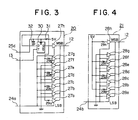
- the "55 H " memory circuit 20 comprises non-inverter circuits 27a to 27h which are respectively provided corresponding to 8 bits from a least significant bit LSB to a most significant bit MSB of the data bus 12, pull-up resistances 29a, 29c, 29e and 29g which are respectively connected to the non-inverter circuits 27a, 27c, 27e and 27g of the bits in odd numbers counted from the LSB, and a latch circuit 30 connected to the non-inverter circuit 27h of the MSB.
- the latch circuit 30 forms a change means in which a 5-V power source, the output line 25d of the inverter circuit 25a, the write-enable signal line 13 and the non-inverter circuit 27h are connected to the input terminal D, the (reset) terminal R, the input terminal T and the output terminal Q, respectively.
- the latch circuit 30 serves to latch-output to the output terminal Q the value of D input at the edge of rise of the input terminal T.
- the "AA H " memory circuit 21 comprises non-inverter circuits 28a to 28h provided corresponding to 8 bits from the LSB to the MSB of the data bus 12, and pull-up resistances 29b, 29d, 29f and 29h which are connected to the non-inverter circuits 28b, 28d, 28f and 28h of the bits in even numbers counted from the LSB.
- the "AA H " (second known data) of the input to the non-inverter circuits 28a to 28h is coded in the manner of hexadecimal representation, as shown in Table 3.
- the memory device A is mounted to a terminal equipment B through the connector 35.
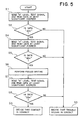
- the terminal equipment B has the function of supplying a power voltage to the power input line 7 of the memory device A and confirming the connection of the connector 35 in accordance with the flow chart described below and shown in Fig. 5.
- Step S1 the terminal equipment B first specifies the most significant address (all the bits are in the "H” level) in the address bus 10 while sending an "H" level test signal to the contact confirmation/control circuit 15 over the test signal line 16, as well as reading the most significant address by sending an "L" level control signal to each of the card-enable signal line 14 and the output-enable signal line 26 of the control bus 11.
- the terminal equipment B first specifies the most significant address (all the bits are in the "H” level) in the address bus 10 while sending an "H" level test signal to the contact confirmation/control circuit 15 over the test signal line 16, as well as reading the most significant address by sending an "L" level control signal to each of the card-enable signal line 14 and the output-enable signal line 26 of the control bus 11.
- Fig. 6 is a drawing which shows the timing of a signal in each unit of the contact confirmation/control circuit 15 during this process.
- Step S2 the terminal equipment B then confirms that the data read is "AA H ", and if the data is not "AA H ", it is decided in Step S3 that a trouble occurs in the contact of the connector 35.
- the "H" level signal output to the output line 24b of the AND circuit 34b is inverted by the inverter circuit 25a and then input to the terminal R of the latch circuit 30 of the "55 H " memory circuit 20 so that the latch circuit 30 is reset, with the output terminal Q being in the "L" level.
- Step S4 the terminal equipment B specifies again the least significant address (all the bits are in the "L" level) in the address bus 10 while sending an "H" level test signal to the contact confirmation/control circuit 15 over the test signal line 16, as well as reading the least significant address by sending an "L" level control signal to each of the card- enable signal line 14 and the output-enable signal line 26 of the control bus 11.
- Step S5 the terminal equipment B confirms that the data read is "55 H ", and if the data is not “55 H “, it is decided in Step S3 that trouble occurs in the contact of the connector 35.
- Step S6 pseudo writing is performed by outputting an "H” level pulses to the write-enable signal line 13.
- the Q output becomes the "H” level at the edge of rise of the write-enable signal which is input to the input terminal T of the latch circuit 30 of the "55 H " memory circuit 20 whereby "D5H” is coded.
- Step S7 the least significant address is then read in the same way as in Step S4.
- the terminal equipment B confirms that the read data is "D5 H ", and if the data is not "D5H", it is decided in Step S3 that trouble occurs in the contact of the connector 35. While if it is confirmed that the data is "D5 H ", it is decided in Step S9 that the connector 35 is accurately connected, and an access to the RAM 1 of the memory device A shown in Fig. 1 is started. Although the access to the RAM 1 is performed in the state wherein the test signal of the test signal line 16 is the "L" level, the access is the same as the access to the conventional memory device shown in Fig. 7 and is not described below.
- Step S3 When trouble occurs in the contact of the connector 35, in Step S3, after the cause of the trouble in the contact has been removed, and the connector 35 has been connected again, the contact is confirmed again in accordance with the flow chart shown in Fig. 5.
- An address bus of more significant than the address bus required for accessing to the RAM 1 or an input/output port may be utilized as the test signal line 16 in place of the use of an independent signal line as the test signal line 16.
- the full-address bus "L" coincidence circuit 17 and the full-address bus “H” coincidence circuit 18 can be easily constructed by using OR circuits, NOR circuits, AND circuits, digital comparators or the like.
- the data bus 12 comprises 8 bits, even if it comprises 16 bits or other bits, the same memory device can be formed.
- the contact confirmation/control circuit 15 may be constructed by using general IC or dedicated IC or may be incorporated in dedicated IC together with the buffer circuit 2.
- the first and second known data are not limited to "55 H” and "AA H ", other data may be used.
- the internal memory may be a semiconductor memory other than the static RAM 1.
- a nonvolatile memory is used as the internal memory, the battery 4, the current limiting resistance 5 and the reverse charge preventing diode 6 which are provided for keeping the data stored are not required
Landscapes
- Engineering & Computer Science (AREA)
- General Engineering & Computer Science (AREA)
- Theoretical Computer Science (AREA)
- Power Engineering (AREA)
- Computer Hardware Design (AREA)
- Quality & Reliability (AREA)
- Physics & Mathematics (AREA)
- General Physics & Mathematics (AREA)
- Techniques For Improving Reliability Of Storages (AREA)
Applications Claiming Priority (2)
| Application Number | Priority Date | Filing Date | Title |
|---|---|---|---|
| JP284855/89 | 1989-11-02 | ||
| JP1284855A JPH03147161A (ja) | 1989-11-02 | 1989-11-02 | 携帯型半導体記憶装置 |
Publications (3)
| Publication Number | Publication Date |
|---|---|
| EP0426270A2 true EP0426270A2 (fr) | 1991-05-08 |
| EP0426270A3 EP0426270A3 (en) | 1992-01-02 |
| EP0426270B1 EP0426270B1 (fr) | 1995-12-27 |
Family
ID=17683904
Family Applications (1)
| Application Number | Title | Priority Date | Filing Date |
|---|---|---|---|
| EP90304512A Expired - Lifetime EP0426270B1 (fr) | 1989-11-02 | 1990-04-26 | Dispositif de mémoire à semi-conducteurs portable |
Country Status (4)
| Country | Link |
|---|---|
| US (1) | US5025420A (fr) |
| EP (1) | EP0426270B1 (fr) |
| JP (1) | JPH03147161A (fr) |
| DE (1) | DE69024462T2 (fr) |
Cited By (1)
| Publication number | Priority date | Publication date | Assignee | Title |
|---|---|---|---|---|
| EP0971290A1 (fr) * | 1998-07-10 | 2000-01-12 | Kabushiki Kaisha Bandai | Dispositif electronique avec protection de cartouche amovible |
Families Citing this family (4)
| Publication number | Priority date | Publication date | Assignee | Title |
|---|---|---|---|---|
| JPH03248249A (ja) * | 1990-02-27 | 1991-11-06 | Mitsubishi Electric Corp | Icメモリカード |
| US5216637A (en) * | 1990-12-07 | 1993-06-01 | Trw Inc. | Hierarchical busing architecture for a very large semiconductor memory |
| US5948085A (en) * | 1996-08-08 | 1999-09-07 | Thomson Consumer Electronics, Inc. | Bus voltage detection and protection |
| DE102013206147B4 (de) * | 2013-04-08 | 2022-06-09 | Beckhoff Automation Gmbh | Dongle-Modul und Automatisierungssystem |
Family Cites Families (3)
| Publication number | Priority date | Publication date | Assignee | Title |
|---|---|---|---|---|
| JPS58118078A (ja) * | 1981-12-29 | 1983-07-13 | Fanuc Ltd | メモリカセツトの信号・電源供給方式 |
| US4485472A (en) * | 1982-04-30 | 1984-11-27 | Carnegie-Mellon University | Testable interface circuit |
| JPH0769759B2 (ja) * | 1988-09-08 | 1995-07-31 | 三菱電機株式会社 | メモリカード用接続機構 |
-
1989
- 1989-11-02 JP JP1284855A patent/JPH03147161A/ja active Pending
-
1990
- 1990-01-16 US US07/465,497 patent/US5025420A/en not_active Expired - Lifetime
- 1990-04-26 EP EP90304512A patent/EP0426270B1/fr not_active Expired - Lifetime
- 1990-04-26 DE DE69024462T patent/DE69024462T2/de not_active Expired - Fee Related
Cited By (2)
| Publication number | Priority date | Publication date | Assignee | Title |
|---|---|---|---|---|
| EP0971290A1 (fr) * | 1998-07-10 | 2000-01-12 | Kabushiki Kaisha Bandai | Dispositif electronique avec protection de cartouche amovible |
| CN1123829C (zh) * | 1998-07-10 | 2003-10-08 | 株式会社万代 | 电子设备 |
Also Published As
| Publication number | Publication date |
|---|---|
| EP0426270A3 (en) | 1992-01-02 |
| JPH03147161A (ja) | 1991-06-24 |
| EP0426270B1 (fr) | 1995-12-27 |
| DE69024462T2 (de) | 1996-08-22 |
| DE69024462D1 (de) | 1996-02-08 |
| US5025420A (en) | 1991-06-18 |
Similar Documents
| Publication | Publication Date | Title |
|---|---|---|
| US4587640A (en) | Cassette type semiconductor memory device | |
| KR100336530B1 (ko) | 기록 및 판독 가능한 집적 회로의 버스 터미널을테스트하기 위한 방법 | |
| EP0184737A2 (fr) | Dispositif de mémoire à semi-conducteur ayant une fonction de détection et de correction d'erreur | |
| EP0399258A3 (fr) | Dispositif de mémoire à semi-conducteurs avec fonction autocorrectrice | |
| US5157634A (en) | Dram having extended refresh time | |
| US5860134A (en) | Memory system with memory presence and type detection using multiplexed memory line function | |
| US4580248A (en) | Electronic apparatus with memory backup system | |
| US6724678B2 (en) | Nonvolatile semiconductor memory unit | |
| EP0426270B1 (fr) | Dispositif de mémoire à semi-conducteurs portable | |
| US5765188A (en) | Memory presence and type detection using multiplexed memory select line | |
| US6796501B2 (en) | Smart card reader circuit and method of monitoring | |
| US6687168B2 (en) | Method for writing data bits to a memory array | |
| US5436862A (en) | IC card including multiple connectors providing memory write production | |
| JP2960752B2 (ja) | 半導体記憶装置 | |
| US5943277A (en) | Apparatus and method for recognizing the state of connection of terminals | |
| US5797024A (en) | PC card | |
| EP0449052A2 (fr) | Procédé et appareil de test de parité pour une puce de mémoire | |
| US5134384A (en) | Data coincidence detecting circuit | |
| US6563344B2 (en) | Buffer circuit for the reception of a clock signal | |
| JPH06195863A (ja) | データ伝送装置 | |
| US5404475A (en) | Memory apparatus comprising memory cards with a side detecting signal pin and address assignment circuitry | |
| US5557233A (en) | Filter for computer bus signals | |
| US5399848A (en) | Portable type semiconductor storage apparatus | |
| US5867431A (en) | Memory device and method of controlling the same | |
| US6094091A (en) | Interface circuit capable of preventing reflected waves and glitches |
Legal Events
| Date | Code | Title | Description |
|---|---|---|---|
| PUAI | Public reference made under article 153(3) epc to a published international application that has entered the european phase |
Free format text: ORIGINAL CODE: 0009012 |
|
| 17P | Request for examination filed |
Effective date: 19901212 |
|
| AK | Designated contracting states |
Kind code of ref document: A2 Designated state(s): DE FR GB |
|
| PUAL | Search report despatched |
Free format text: ORIGINAL CODE: 0009013 |
|
| AK | Designated contracting states |
Kind code of ref document: A3 Designated state(s): DE FR GB |
|
| 17Q | First examination report despatched |
Effective date: 19940223 |
|
| GRAA | (expected) grant |
Free format text: ORIGINAL CODE: 0009210 |
|
| AK | Designated contracting states |
Kind code of ref document: B1 Designated state(s): DE FR GB |
|
| REF | Corresponds to: |
Ref document number: 69024462 Country of ref document: DE Date of ref document: 19960208 |
|
| REG | Reference to a national code |
Ref country code: GB Ref legal event code: 727 |
|
| REG | Reference to a national code |
Ref country code: GB Ref legal event code: 727A |
|
| ET | Fr: translation filed | ||
| REG | Reference to a national code |
Ref country code: GB Ref legal event code: 727B |
|
| REG | Reference to a national code |
Ref country code: GB Ref legal event code: SP |
|
| PLBE | No opposition filed within time limit |
Free format text: ORIGINAL CODE: 0009261 |
|
| STAA | Information on the status of an ep patent application or granted ep patent |
Free format text: STATUS: NO OPPOSITION FILED WITHIN TIME LIMIT |
|
| 26N | No opposition filed | ||
| REG | Reference to a national code |
Ref country code: GB Ref legal event code: IF02 |
|
| PGFP | Annual fee paid to national office [announced via postgrant information from national office to epo] |
Ref country code: FR Payment date: 20060410 Year of fee payment: 17 |
|
| PGFP | Annual fee paid to national office [announced via postgrant information from national office to epo] |
Ref country code: DE Payment date: 20060420 Year of fee payment: 17 |
|
| PGFP | Annual fee paid to national office [announced via postgrant information from national office to epo] |
Ref country code: GB Payment date: 20060426 Year of fee payment: 17 |
|
| GBPC | Gb: european patent ceased through non-payment of renewal fee |
Effective date: 20070426 |
|
| PG25 | Lapsed in a contracting state [announced via postgrant information from national office to epo] |
Ref country code: DE Free format text: LAPSE BECAUSE OF NON-PAYMENT OF DUE FEES Effective date: 20071101 |
|
| PG25 | Lapsed in a contracting state [announced via postgrant information from national office to epo] |
Ref country code: GB Free format text: LAPSE BECAUSE OF NON-PAYMENT OF DUE FEES Effective date: 20070426 |
|
| PG25 | Lapsed in a contracting state [announced via postgrant information from national office to epo] |
Ref country code: FR Free format text: LAPSE BECAUSE OF NON-PAYMENT OF DUE FEES Effective date: 20070430 |