EP0426282B1 - Programmierbare logische Vorrichtung - Google Patents
Programmierbare logische Vorrichtung Download PDFInfo
- Publication number
- EP0426282B1 EP0426282B1 EP90309521A EP90309521A EP0426282B1 EP 0426282 B1 EP0426282 B1 EP 0426282B1 EP 90309521 A EP90309521 A EP 90309521A EP 90309521 A EP90309521 A EP 90309521A EP 0426282 B1 EP0426282 B1 EP 0426282B1
- Authority
- EP
- European Patent Office
- Prior art keywords
- floating gate
- transistor
- signal line
- row
- programming
- Prior art date
- Legal status (The legal status is an assumption and is not a legal conclusion. Google has not performed a legal analysis and makes no representation as to the accuracy of the status listed.)
- Expired - Lifetime
Links
Images


Classifications
-
- G—PHYSICS
- G11—INFORMATION STORAGE
- G11C—STATIC STORES
- G11C16/00—Erasable programmable read-only memories
-
- G—PHYSICS
- G11—INFORMATION STORAGE
- G11C—STATIC STORES
- G11C16/00—Erasable programmable read-only memories
- G11C16/02—Erasable programmable read-only memories electrically programmable
- G11C16/04—Erasable programmable read-only memories electrically programmable using variable threshold transistors, e.g. FAMOS
- G11C16/0408—Erasable programmable read-only memories electrically programmable using variable threshold transistors, e.g. FAMOS comprising cells containing floating gate transistors
- G11C16/0433—Erasable programmable read-only memories electrically programmable using variable threshold transistors, e.g. FAMOS comprising cells containing floating gate transistors comprising cells containing a single floating gate transistor and one or more separate select transistors
-
- H—ELECTRICITY
- H10—SEMICONDUCTOR DEVICES; ELECTRIC SOLID-STATE DEVICES NOT OTHERWISE PROVIDED FOR
- H10B—ELECTRONIC MEMORY DEVICES
- H10B69/00—Erasable-and-programmable ROM [EPROM] devices not provided for in groups H10B41/00 - H10B63/00, e.g. ultraviolet erasable-and-programmable ROM [UVEPROM] devices
Definitions
- the present invention relates generally to integrated circuits, and more specifically to an electrically erasable programmable read only memory circuit.
- EEPROM Electrically erasable programmable read only memory
- EEPROM memory cells can be used in some types of programmable logic devices to store configuration information for such devices. They are also used to define switch connections in a AND-OR array, such as used in programmable logic arrays and more sophisticated devices which are programmed in a similar way.
- EEPROM cells each containing a memory bit, are programmed ON using a high voltage signal to inject charge onto a floating gate. These cells are programmed off by reversing the polarity of the high voltage, and removing charge from the floating gate. Once programmed, the charge on the floating gate causes the floating gate device to behave as a field effect transistor which remains switched either on or off.
- EP-A-0284724 (Toshiba) is directed to providing a nonvolatile memory device, and in particular to the provision of simple peripheral circuits including the sense amplifier.
- the document describes a so-called three transistor cell where a floating gate transistor is connected between a write select transistor and a read select transistor.
- the cell can operate in a data erase mode, data write mode and data read mode according to different voltages applied to the transistors.
- the read select and write select transistors are of a similar configuration, and thus in particular in the case of the read select transistors present a significant capacitance on the read select lines.
- the addition of a third transistor as shown in Figures 5 and 7 has as its object to allow a 5V voltage on the read line of the memory cell, instead of 1V previously, without causing a so-called "soft write".
- Read/write transistors used to access the floating gate transistors are among those which must be able to handle the higher programming voltages.
- the circuitry used to drive these transistors must be fabricated using N-channel technology.
- CMOS circuitry cannot be used to drive the read/write transistors because the higher voltage used therein makes the drive circuitry more susceptible to latch-up problems.
- N-channel technology is used in the driving circuitry, the maximum signal which can be applied to turn on the read/write transistors during normal operation is V cc -V Tn . This lower driving voltage provides less signal margin for the read/write transistors, and results in slower operation. Bootstrapping can be used to raise the signal back to V cc , but the necessary circuitry adds delay.
- a programmable logic device having an AND-OR array containing input signal'rows and product term signal lines, wherein each junction of a row with a product term signal line contains a switching element, said switching element comprising:
- the device preferably comprises means for, during a read operation, switching said programming transistor on at all times, connecting the supply voltage to ground, and switching said select transistor on in response to a high voltage applied to its select control input, whereby, when said select transistor is switched on, the product term signal line is connected to ground if said floating gate transistor is controlled to be on by the floating gate, and the product term signal line is not connected to ground through the floating gate transistor otherwise.
- Input signal lines 12 , 14 carry input signals provided from off chip.
- Input signal lines 12, 14 are connected to input buffers 16, 18 respectively.
- Each input buffer 16, 18 provides a true signal line 20, 22 and a complement signal line 24, 26 .
- Only two input signal lines 12, 14 and input buffers 16, 18 are shown in Figure 1 , but an actual device typically has a much larger number.
- Each of the signal lines 20-26 is connected to a row line 28, 30, 32, 34 .
- Row lines 28 and 30 designated with the signals ROW and ROWB carry complementary signals determined by the input on line 12 .
- row lines 32, 34 contain complementary signals determined by the input on line 14 .
- additional row lines can be used to carry feedback signals from output registers (not shown).
- a product signal line 36 crosses all of the row lines 28-34 , and drives a sense amplifier 38 .
- Sense amplifier 38 generates output signal PT. Only one product signal line 36 is shown, but it is understood that many such lines are included in actual devices. A typical device might include, for example, 44 row lines and 122 product signal lines.
- the signal available on line 36 is determined by programmed connections made between the row lines 28-34 and the product signal lines 36 . Connections are made at the intersections of these lines by using transistor switches.
- a typical transistor switch includes an EEPROM cell which is programmed ON or OFF in order for the connection at any particular point to be made or not made, respectively.
- EEPROM cells are typically built in pairs, with a single EEPROM cell pair 40, 42 having two switches and being programmed to determine the connections between one product signal line 36 and one row and its complement.
- a device having 44 row lines (22 pairs) and 122 product signal lines would include 2684 EEPROM cell pairs in the AND-OR array.
- Floating gate devices 44, 46 are connected to product signal line 36 .
- Each device contains a floating gate node 48 which is capacitively coupled to a programming voltage supply line 50 .
- Read/write transistors 52, 54 are connected between floating gate devices 44, 46, respectively, and product term ground signal line 56 .
- signal line 56 is connected to device ground.
- the signals ROW and ROWB are used to switch read/write transistors 52, 54 respectively. As described above, the signals ROW and ROWB are complementary, so that only one of the read/write transistors 52, 54 is switched on at all times.
- the floating gate devices 44, 46 are programmed ON by storing charge on their respective nodes 48 . If floating gate device 44 is programmed ON, and ROW is high, output signal line 36 is connected to ground through floating gate device 44 and transistor 52 . If floating gate device 44 is programmed OFF, device 44 is non-conductive and signal line 36 is not connected to ground. Floating gate device 46 and transistor 54 operate on a similar fashion.
- Floating gate device 44 is programmed ON by tunneling charge onto the floating gate node 48 through a thin gate oxide. This is accomplished by driving the signals ROW and PTG to a super voltage while grounding the signal MCGO.
- the super voltage is substantially higher than the normal operating voltage of the programmable logic device. For example, for a device which normally operates using a supply voltage of 5 volts, the programming super voltage is typically 12-18 volts.
- signal line 56 With MCGO at ground, and ROW and PTG at the super voltage, signal line 56 has a net positive charge on it with respect to the floating gate node 48 . Electrons flow from node 48 to signal line 56 through the gate oxide of floating gate device 44 and through transistor 52 . After this tunneling has been completed signal line 50 is connected to ground, leaving a net positive charge on floating gate node 48 . This causes floating gate device 44 to be ON, providing a DC current path between read/write transistor 52 and output signal line 36 .
- Figure 3 illustrates a portion of a programmable logic device having a plurality of prior art EEPROM cell pairs 40 connected to a product signal line 36 .
- 22 different true and complement row pairs are connected to each signal line 36 .
- the floating gate devices 44 and 46 have a relatively large capacitance regardless of whether they are programmed ON or OFF. Since all of the floating gate devices 44, 46 are connected to the product signal line 36, a relatively large lumped capacitance is attached to such signal line 36 . As will be appreciated by those skilled in the art, the existence of this capacitance greatly decreases the speed at which the voltage level of line 36 can change. If the combination of floating gate device programming and ROW inputs causes the voltage level on line 36 to change from high to low, or vice versa, the capacitive load provided by the floating gate devices 44, 46 limits the rate of which such change can occur.
- the read/write transistors 52, 54 must have a larger than minimum size because of the super voltage signals applied across their source/drains when the gate is low during programming. Larger transistors induce a larger capacitive load than do smaller transistors, which further increases the time required for the signal on output line 36 to change state.
- the signals ROW and ROWB are the inverse of each other. Thus, one signal rises when the other signal falls. It is preferable to have both signals change symmetrically in order to ensure equivalent data access times in both directions.
- the cell pair 40 if only one of the floating gate devices 44, 46 is programmed ON, there will exist a unidirectional coupling on signal line 36 when the signals ROW and ROWB switch.
- Cell pair 60 includes connections to product term output signal line 62 and product term ground 64 . These two signal lines 62, 64 function in a manner substantially equivalent to their counterpart signal lines 36 and 56 in the prior art cell pair 40 .
- Cell pair 60 includes floating gate devices 66 and 68, each of which has a floating gate node 70 .
- the floating gate nodes 70 are capacitively coupled to programming voltage supply line 72, driven by the signal MCGO.
- Floating gate devices 66, 68 are connected to the output signal line 62 through select, or read, transistors 74 and 76 respectively. Floating gate devices 66, 68 are connected to the product term ground signal line 64 through decode, or programming, transistors 78 and 80 respectively. Read transistors 74, 76 are driven by the ROW and ROWB signals, respectively, and the programming transistors 78, 80 are driven by the decode signals DECA and DECB, respectively.
- the floating gate devices 66, 68 are programmed in a similar fashion to that used for the prior art devices. To program the floating gate devices ON, MCGO is grounded and PTG is driven to the super voltage. For each floating gate device 66, 68 which is to be programmed ON, the corresponding decode signal DECA or DECB, is also driven to the super voltage. This causes tunneling to produce a net positive charge on the floating gate node 70 of the corresponding floating gate device 66 or 68 .
- MCGO is driven to the super voltage while PTG is grounded.
- DECA and DECB are driven to the super voltage for all of the associated floating gate devices 66, 68 which are to be programmed OFF. Tunneling causes a net negative charge to occur on the selected floating gate nodes 70 .
- both MCGO and PTG are grounded.
- both signals DECA and DECB are driven to the positive supply voltage at all times.
- a depletion-mode N-channel device (not shown) can be used to bring the DECA and DECB signals up to V cc .
- Such a device adds some delay to the driving circuitry, but this does not matter since DECA and DECB never change during normal operation of the device. Since only N-channel devices can be used in the driving circuitry for the signals DECA and DECB, the signals will actually have a voltage limited to V cc -V Tn . This is sufficient to bias programming transistors 78, 80 ON, and has no adverse effect because these transistors are never switched during normal operation.
- ROW and ROWB are complements, one of the select transistors 74 or 76 will always be ON. If the associated floating gate device 66 or 68 is programmed ON, signal line 62 will be connected to ground. If the associated floating gate device 66, 68 is programmed OFF, signal line 62 will not be connected to ground.
- High voltages are applied to the floating gate devices 66, 68 for programming as in the usual case. High voltages are also applied to programming transistors 78, 80, which must be of a larger size for the reasons described above.
- the select transistor 74, 76 which are the ones actually switched during normal operation of the device, are never driven using high programming voltages. Therefore, these devices may be made smaller, resulting in faster switching during normal operation.
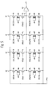
- a plurality of improved cells 60 are shown connected to an output signal line 62 .
- Signal line 62 is connected to sense amplifier 82, which drives the signal PT.
- the sense amplifier 82 includes a resistive pull-up element (not shown), which pulls the voltage on signal line 62 up to a one level when none of the cell pairs 60 contains a DC path to ground.
- CMOS circuitry can be used to drive them. This allows the signals ROW and ROWB to actually be driven all the way to the supply voltage. This larger voltage swing than that found in the prior art devices improves their signal margin and allows faster switching times. In addition, there is no high voltage driver circuitry connected to the ROW and ROWB signals. This results in a lower capacitance in the driving circuitry, allowing ROW and ROWB to switch faster and contribution to further decreased switching times of the device.
Landscapes
- Engineering & Computer Science (AREA)
- Microelectronics & Electronic Packaging (AREA)
- Read Only Memory (AREA)
- Non-Volatile Memory (AREA)
- Logic Circuits (AREA)
Claims (2)
- Programmierbare Logikvorrichtung mit einem UND-ODER-Array, das Eingabesignalreihen und Produktterm-Signalleitungen beinhaltet, bei welcher jede Verbindung einer Reihe mit einer Produktterm-Signalleitung ein Schaltelement beinhaltet, wobei das Schaltelement folgendes aufweist:einen Auswahltransistor (74) mit einem Source-/Drain-Anschluß, der mit einer Produktterm-Signalleitung (PT) verbunden ist, und mit einem Steueranschluß, um eine Auswahlsteuereingabe auf einer Eingangssignalreihe (ROW) zu empfangen;einen Floating-Gate-Transistor (66) mit einem Source-/Drain-Anschluß, der mit einem anderen Source-/Drain-Anschluß des Auswahltransistors (74) verbunden ist, wobei der Betrieb des Floating-Gate-Transistors (66) durch eine Ladung gesteuert wird, die auf einem Floating-Gate (70) durch ein Gateoxid gespeichert ist, das für ein Ladungstunneln geeignet ist, und wobei ein Einschalten des Auswahltransistors (74) in Antwort auf die Auswahlsteuerungseingabe (ROW) bewirkt, daß die Produktterm-Signalleitung (PT) die Anwesenheit oder Abwesenheit von Ladung auf dem Floating-Gate (70) anzeigt, wodurch das Schaltelement gelesen wird; undeinen Programmiertransistor (78) mit einem Source-/Drain-Anschluß, der mit dem anderen Source-/Drain-Anschluß des Floating-Gate-Transistors (66) verbunden ist, mit einem anderen Source-/Drain-Anschluß, der mit einer Versorgungsspannung (PTG) verbunden ist, und mit einem Steueranschluß zum Empfangen einer Programmier-Steuereingabe (DECA), wobei eine Ladung, die auf dem Floating-Gate (70) gespeichert ist, von der Versorgungsspannung (PTG) durch den Programmiertransistor (78) bereitgestellt wird; wobei der Programmiertransistor angepaßt ist, um Programmierspannungen zu empfangen, die höher sind als eine normale Betriebsspannung, und wobei der Auswahltransistor (74) physikalisch kleiner ist als der Programmiertransistor (78), wodurch die Kapazität verringert wird, die durch die Produktterm-Signalleitung (PT) dargestellt wird.
- Vorrichtung nach Anspruch 1, die eine Einrichtung aufweist, um während einer Leseoperation den Programmiertransistor (78) zu allen Zeiten einzuschalten, die Versorgungsspannung (PTG) mit der Erde bzw. Masse zu verbinden und den Auswahltransistor (74) in Antwort auf eine Hochspannung einzuschalten, die an seinen Auswahl-Steuereingang (ROW) angelegt wird, wodurch, wenn der Auswahltransistor (74) eingeschaltet wird, die Produktterm-Signalleitung (PT) mit der Erde bzw. der Masse verbunden wird, falls der Floating-Gate-Transistor (66) durch das Floating-Gate so gesteuert wird, daß er EIN ist, und ansonsten die Produktterm-Signalleitung (PT) nicht mit der Masse über den Floating-Gate-Transistor verbunden wird.
Applications Claiming Priority (2)
| Application Number | Priority Date | Filing Date | Title |
|---|---|---|---|
| US429308 | 1989-10-31 | ||
| US07/429,308 US5170373A (en) | 1989-10-31 | 1989-10-31 | Three transistor eeprom cell |
Publications (3)
| Publication Number | Publication Date |
|---|---|
| EP0426282A2 EP0426282A2 (de) | 1991-05-08 |
| EP0426282A3 EP0426282A3 (en) | 1992-05-13 |
| EP0426282B1 true EP0426282B1 (de) | 1997-10-29 |
Family
ID=23702691
Family Applications (1)
| Application Number | Title | Priority Date | Filing Date |
|---|---|---|---|
| EP90309521A Expired - Lifetime EP0426282B1 (de) | 1989-10-31 | 1990-08-30 | Programmierbare logische Vorrichtung |
Country Status (5)
| Country | Link |
|---|---|
| US (1) | US5170373A (de) |
| EP (1) | EP0426282B1 (de) |
| JP (1) | JPH03210818A (de) |
| KR (1) | KR910008732A (de) |
| DE (1) | DE69031648T2 (de) |
Cited By (11)
| Publication number | Priority date | Publication date | Assignee | Title |
|---|---|---|---|---|
| US6911682B2 (en) | 2001-12-28 | 2005-06-28 | Nantero, Inc. | Electromechanical three-trace junction devices |
| US6919592B2 (en) | 2001-07-25 | 2005-07-19 | Nantero, Inc. | Electromechanical memory array using nanotube ribbons and method for making same |
| US6942921B2 (en) | 2001-07-25 | 2005-09-13 | Nantero, Inc. | Nanotube films and articles |
| US7120047B2 (en) | 2001-07-25 | 2006-10-10 | Segal Brent M | Device selection circuitry constructed with nanotube technology |
| US7264990B2 (en) | 2001-07-25 | 2007-09-04 | Nantero, Inc. | Methods of nanotubes films and articles |
| US7274078B2 (en) | 2001-07-25 | 2007-09-25 | Nantero, Inc. | Devices having vertically-disposed nanofabric articles and methods of making the same |
| US7304357B2 (en) | 2001-07-25 | 2007-12-04 | Nantero, Inc. | Devices having horizontally-disposed nanofabric articles and methods of making the same |
| US7335395B2 (en) | 2002-04-23 | 2008-02-26 | Nantero, Inc. | Methods of using pre-formed nanotubes to make carbon nanotube films, layers, fabrics, ribbons, elements and articles |
| US7342818B2 (en) | 2001-07-25 | 2008-03-11 | Nantero, Inc. | Hybrid circuit having nanotube electromechanical memory |
| US7560136B2 (en) | 2003-01-13 | 2009-07-14 | Nantero, Inc. | Methods of using thin metal layers to make carbon nanotube films, layers, fabrics, ribbons, elements and articles |
| US7566478B2 (en) | 2001-07-25 | 2009-07-28 | Nantero, Inc. | Methods of making carbon nanotube films, layers, fabrics, ribbons, elements and articles |
Families Citing this family (20)
| Publication number | Priority date | Publication date | Assignee | Title |
|---|---|---|---|---|
| DE4121053C2 (de) * | 1991-06-26 | 1995-10-19 | Eurosil Electronic Gmbh | Speicherzelle mit Floating-Gate-Transistor |
| US5930638A (en) * | 1993-07-12 | 1999-07-27 | Peregrine Semiconductor Corp. | Method of making a low parasitic resistor on ultrathin silicon on insulator |
| US5863823A (en) * | 1993-07-12 | 1999-01-26 | Peregrine Semiconductor Corporation | Self-aligned edge control in silicon on insulator |
| US5864162A (en) * | 1993-07-12 | 1999-01-26 | Peregrine Seimconductor Corporation | Apparatus and method of making a self-aligned integrated resistor load on ultrathin silicon on sapphire |
| JPH09512658A (ja) * | 1994-04-29 | 1997-12-16 | アトメル・コーポレイション | 高速で、不揮発性の電気的にプログラム可能で、かつ消去可能なセルおよび方法 |
| US5596524A (en) * | 1995-04-21 | 1997-01-21 | Advanced Micro Devices, Inc. | CMOS memory cell with gate oxide of both NMOS and PMOS transistors as tunneling window for program and erase |
| US5754471A (en) * | 1995-06-06 | 1998-05-19 | Advanced Micro Devices, Inc. | Low power CMOS array for a PLD with program and erase using controlled avalanche injection |
| US5742542A (en) * | 1995-07-03 | 1998-04-21 | Advanced Micro Devices, Inc. | Non-volatile memory cells using only positive charge to store data |
| US5581501A (en) * | 1995-08-17 | 1996-12-03 | Altera Corporation | Nonvolatile SRAM cells and cell arrays |
| US5587945A (en) * | 1995-11-06 | 1996-12-24 | Advanced Micro Devices, Inc. | CMOS EEPROM cell with tunneling window in the read path |
| US6005806A (en) * | 1996-03-14 | 1999-12-21 | Altera Corporation | Nonvolatile configuration cells and cell arrays |
| US5646901A (en) * | 1996-03-26 | 1997-07-08 | Advanced Micro Devices, Inc. | CMOS memory cell with tunneling during program and erase through the NMOS and PMOS transistors and a pass gate separating the NMOS and PMOS transistors |
| US6018476A (en) * | 1996-09-16 | 2000-01-25 | Altera Corporation | Nonvolatile configuration cells and cell arrays |
| US6327182B1 (en) | 1998-06-22 | 2001-12-04 | Motorola Inc. | Semiconductor device and a method of operation the same |
| US6232634B1 (en) | 1998-07-29 | 2001-05-15 | Motorola, Inc. | Non-volatile memory cell and method for manufacturing same |
| US6064595A (en) * | 1998-12-23 | 2000-05-16 | Vantis Corporation | Floating gate memory apparatus and method for selected programming thereof |
| US7430137B2 (en) * | 2004-09-09 | 2008-09-30 | Actel Corporation | Non-volatile memory cells in a field programmable gate array |
| US8320191B2 (en) | 2007-08-30 | 2012-11-27 | Infineon Technologies Ag | Memory cell arrangement, method for controlling a memory cell, memory array and electronic device |
| JP2012191455A (ja) * | 2011-03-10 | 2012-10-04 | Toshiba Corp | 半導体集積回路 |
| JP5771315B2 (ja) * | 2014-06-23 | 2015-08-26 | 株式会社東芝 | 半導体集積回路 |
Family Cites Families (13)
| Publication number | Priority date | Publication date | Assignee | Title |
|---|---|---|---|---|
| NL7905548A (nl) * | 1979-07-17 | 1981-01-20 | Unilever Nv | Vaste koolwaterstofharsen. |
| US4380804A (en) * | 1980-12-29 | 1983-04-19 | Ncr Corporation | Earom cell matrix and logic arrays with common memory gate |
| US4715014A (en) * | 1985-10-29 | 1987-12-22 | Texas Instruments Incorporated | Modified three transistor EEPROM cell |
| JPS62266793A (ja) * | 1986-05-13 | 1987-11-19 | Mitsubishi Electric Corp | 不揮発性半導体記憶装置 |
| JPS63138598A (ja) * | 1986-11-28 | 1988-06-10 | Mitsubishi Electric Corp | 不揮発性半導体記憶装置 |
| JPH0777078B2 (ja) * | 1987-01-31 | 1995-08-16 | 株式会社東芝 | 不揮発性半導体メモリ |
| US5008856A (en) * | 1987-06-29 | 1991-04-16 | Kabushiki Kaisha Toshiba | Electrically programmable nonvolatile semiconductor memory device with NAND cell structure |
| JPH07120719B2 (ja) * | 1987-12-02 | 1995-12-20 | 三菱電機株式会社 | 半導体記憶装置 |
| US4855955A (en) * | 1988-04-08 | 1989-08-08 | Seeq Technology, Inc. | Three transistor high endurance eeprom cell |
| US5005155A (en) * | 1988-06-15 | 1991-04-02 | Advanced Micro Devices, Inc. | Optimized electrically erasable PLA cell for minimum read disturb |
| US5101378A (en) * | 1988-06-15 | 1992-03-31 | Advanced Micro Devices, Inc. | Optimized electrically erasable cell for minimum read disturb and associated method of sensing |
| US4935698A (en) * | 1989-03-03 | 1990-06-19 | Sprague Electric Company | Sensor having dual Hall IC, pole piece and magnet |
| US4963769A (en) * | 1989-05-08 | 1990-10-16 | Cypress Semiconductor | Circuit for selective power-down of unused circuitry |
-
1989
- 1989-10-31 US US07/429,308 patent/US5170373A/en not_active Expired - Lifetime
-
1990
- 1990-08-30 EP EP90309521A patent/EP0426282B1/de not_active Expired - Lifetime
- 1990-08-30 DE DE69031648T patent/DE69031648T2/de not_active Expired - Fee Related
- 1990-10-22 KR KR1019900016909A patent/KR910008732A/ko not_active Ceased
- 1990-10-31 JP JP2292205A patent/JPH03210818A/ja active Pending
Cited By (15)
| Publication number | Priority date | Publication date | Assignee | Title |
|---|---|---|---|---|
| US7274078B2 (en) | 2001-07-25 | 2007-09-25 | Nantero, Inc. | Devices having vertically-disposed nanofabric articles and methods of making the same |
| US7298016B2 (en) | 2001-07-25 | 2007-11-20 | Nantero, Inc. | Electromechanical memory array using nanotube ribbons and method for making same |
| US6942921B2 (en) | 2001-07-25 | 2005-09-13 | Nantero, Inc. | Nanotube films and articles |
| US7056758B2 (en) | 2001-07-25 | 2006-06-06 | Nantero, Inc. | Electromechanical memory array using nanotube ribbons and method for making same |
| US7120047B2 (en) | 2001-07-25 | 2006-10-10 | Segal Brent M | Device selection circuitry constructed with nanotube technology |
| US7264990B2 (en) | 2001-07-25 | 2007-09-04 | Nantero, Inc. | Methods of nanotubes films and articles |
| US6919592B2 (en) | 2001-07-25 | 2005-07-19 | Nantero, Inc. | Electromechanical memory array using nanotube ribbons and method for making same |
| US7745810B2 (en) | 2001-07-25 | 2010-06-29 | Nantero, Inc. | Nanotube films and articles |
| US7566478B2 (en) | 2001-07-25 | 2009-07-28 | Nantero, Inc. | Methods of making carbon nanotube films, layers, fabrics, ribbons, elements and articles |
| US7335528B2 (en) | 2001-07-25 | 2008-02-26 | Nantero, Inc. | Methods of nanotube films and articles |
| US7304357B2 (en) | 2001-07-25 | 2007-12-04 | Nantero, Inc. | Devices having horizontally-disposed nanofabric articles and methods of making the same |
| US7342818B2 (en) | 2001-07-25 | 2008-03-11 | Nantero, Inc. | Hybrid circuit having nanotube electromechanical memory |
| US6911682B2 (en) | 2001-12-28 | 2005-06-28 | Nantero, Inc. | Electromechanical three-trace junction devices |
| US7335395B2 (en) | 2002-04-23 | 2008-02-26 | Nantero, Inc. | Methods of using pre-formed nanotubes to make carbon nanotube films, layers, fabrics, ribbons, elements and articles |
| US7560136B2 (en) | 2003-01-13 | 2009-07-14 | Nantero, Inc. | Methods of using thin metal layers to make carbon nanotube films, layers, fabrics, ribbons, elements and articles |
Also Published As
| Publication number | Publication date |
|---|---|
| EP0426282A2 (de) | 1991-05-08 |
| JPH03210818A (ja) | 1991-09-13 |
| KR910008732A (ko) | 1991-05-31 |
| EP0426282A3 (en) | 1992-05-13 |
| DE69031648T2 (de) | 1998-03-19 |
| DE69031648D1 (de) | 1997-12-04 |
| US5170373A (en) | 1992-12-08 |
Similar Documents
| Publication | Publication Date | Title |
|---|---|---|
| EP0426282B1 (de) | Programmierbare logische Vorrichtung | |
| US6028787A (en) | Nonvolatile static memory circuit | |
| JP2818803B2 (ja) | プログラム可能な論理装置 | |
| US4953127A (en) | Semiconductor memory having different read and write word line voltage levels | |
| EP0586473B1 (de) | Nicht-fluechtige loeschbare und programmierbare verbindungszelle | |
| EP0840930B1 (de) | Programmierbarer nichtflüchtiger zweiwegschalter für programmierbare logik | |
| US5978263A (en) | Negative voltage switch architecture for a nonvolatile memory | |
| US5267213A (en) | Bias circuitry for content addressable memory cells of a floating gate nonvolatile memory | |
| US6774704B2 (en) | Control circuit for selecting the greater of two voltage signals | |
| JP3375134B2 (ja) | ゼロ電力高速プログラマブル回路装置アーキテクチャ | |
| JPH0562486A (ja) | 集積回路用スイツチ | |
| JPH0715797B2 (ja) | 不揮発性ramメモリを備えたマイクロコンピユ−タ | |
| JP4262678B2 (ja) | メモリマトリクスの複数の横列に対して同時書き込みを行うデバイス | |
| JPH0821849B2 (ja) | 半導体記憶装置 | |
| EP0194091B1 (de) | Programmierbare logische Schaltung mit begrenzten Leserströmen | |
| US5138198A (en) | Integrated programmable logic device with control circuit to power down unused sense amplifiers | |
| JPH0814995B2 (ja) | 半導体メモリ | |
| US6512694B2 (en) | NAND stack EEPROM with random programming capability | |
| EP0317939B1 (de) | Eingangsschaltung, die in eine Halbleiteranlage eingegliedert ist | |
| JPH03105797A (ja) | デコーダ回路 | |
| JPS63271798A (ja) | 消去可能なプログラマブル論理装置 | |
| US5973967A (en) | Page buffer having negative voltage level shifter | |
| US4788460A (en) | Circuit arrangement of sense amplifier for rapid evaluation of logic state | |
| US5198998A (en) | Erasable programmable read only memory | |
| US5757713A (en) | Adjustable write voltage circuit for SRAMS |
Legal Events
| Date | Code | Title | Description |
|---|---|---|---|
| PUAI | Public reference made under article 153(3) epc to a published international application that has entered the european phase |
Free format text: ORIGINAL CODE: 0009012 |
|
| AK | Designated contracting states |
Kind code of ref document: A2 Designated state(s): DE FR GB IT |
|
| PUAL | Search report despatched |
Free format text: ORIGINAL CODE: 0009013 |
|
| AK | Designated contracting states |
Kind code of ref document: A3 Designated state(s): DE FR GB IT |
|
| 17P | Request for examination filed |
Effective date: 19921029 |
|
| 17Q | First examination report despatched |
Effective date: 19941216 |
|
| GRAG | Despatch of communication of intention to grant |
Free format text: ORIGINAL CODE: EPIDOS AGRA |
|
| GRAH | Despatch of communication of intention to grant a patent |
Free format text: ORIGINAL CODE: EPIDOS IGRA |
|
| GRAH | Despatch of communication of intention to grant a patent |
Free format text: ORIGINAL CODE: EPIDOS IGRA |
|
| GRAA | (expected) grant |
Free format text: ORIGINAL CODE: 0009210 |
|
| AK | Designated contracting states |
Kind code of ref document: B1 Designated state(s): DE FR GB IT |
|
| REF | Corresponds to: |
Ref document number: 69031648 Country of ref document: DE Date of ref document: 19971204 |
|
| ITF | It: translation for a ep patent filed | ||
| ET | Fr: translation filed | ||
| PLBE | No opposition filed within time limit |
Free format text: ORIGINAL CODE: 0009261 |
|
| STAA | Information on the status of an ep patent application or granted ep patent |
Free format text: STATUS: NO OPPOSITION FILED WITHIN TIME LIMIT |
|
| PGFP | Annual fee paid to national office [announced via postgrant information from national office to epo] |
Ref country code: DE Payment date: 19980907 Year of fee payment: 9 |
|
| 26N | No opposition filed | ||
| PG25 | Lapsed in a contracting state [announced via postgrant information from national office to epo] |
Ref country code: DE Free format text: LAPSE BECAUSE OF NON-PAYMENT OF DUE FEES Effective date: 20000601 |
|
| REG | Reference to a national code |
Ref country code: GB Ref legal event code: IF02 |
|
| PGFP | Annual fee paid to national office [announced via postgrant information from national office to epo] |
Ref country code: GB Payment date: 20020828 Year of fee payment: 13 |
|
| PGFP | Annual fee paid to national office [announced via postgrant information from national office to epo] |
Ref country code: FR Payment date: 20030808 Year of fee payment: 14 |
|
| PG25 | Lapsed in a contracting state [announced via postgrant information from national office to epo] |
Ref country code: GB Free format text: LAPSE BECAUSE OF NON-PAYMENT OF DUE FEES Effective date: 20030830 |
|
| GBPC | Gb: european patent ceased through non-payment of renewal fee | ||
| PG25 | Lapsed in a contracting state [announced via postgrant information from national office to epo] |
Ref country code: FR Free format text: LAPSE BECAUSE OF NON-PAYMENT OF DUE FEES Effective date: 20050429 |
|
| REG | Reference to a national code |
Ref country code: FR Ref legal event code: ST |
|
| PG25 | Lapsed in a contracting state [announced via postgrant information from national office to epo] |
Ref country code: IT Free format text: LAPSE BECAUSE OF NON-PAYMENT OF DUE FEES;WARNING: LAPSES OF ITALIAN PATENTS WITH EFFECTIVE DATE BEFORE 2007 MAY HAVE OCCURRED AT ANY TIME BEFORE 2007. THE CORRECT EFFECTIVE DATE MAY BE DIFFERENT FROM THE ONE RECORDED. Effective date: 20050830 |