EP0426349A2 - Socle support de circuit intégré de faible hauteur - Google Patents
Socle support de circuit intégré de faible hauteur Download PDFInfo
- Publication number
- EP0426349A2 EP0426349A2 EP90311546A EP90311546A EP0426349A2 EP 0426349 A2 EP0426349 A2 EP 0426349A2 EP 90311546 A EP90311546 A EP 90311546A EP 90311546 A EP90311546 A EP 90311546A EP 0426349 A2 EP0426349 A2 EP 0426349A2
- Authority
- EP
- European Patent Office
- Prior art keywords
- contacts
- chip carrier
- lead
- socket
- leads
- Prior art date
- Legal status (The legal status is an assumption and is not a legal conclusion. Google has not performed a legal analysis and makes no representation as to the accuracy of the status listed.)
- Granted
Links
Images



Classifications
-
- H—ELECTRICITY
- H05—ELECTRIC TECHNIQUES NOT OTHERWISE PROVIDED FOR
- H05K—PRINTED CIRCUITS; CASINGS OR CONSTRUCTIONAL DETAILS OF ELECTRIC APPARATUS; MANUFACTURE OF ASSEMBLAGES OF ELECTRICAL COMPONENTS
- H05K7/00—Constructional details common to different types of electric apparatus
- H05K7/02—Arrangements of circuit components or wiring on supporting structure
- H05K7/10—Plug-in assemblages of components, e.g. IC sockets
- H05K7/1015—Plug-in assemblages of components, e.g. IC sockets having exterior leads
- H05K7/1023—Plug-in assemblages of components, e.g. IC sockets having exterior leads co-operating by abutting, e.g. flat pack
-
- H—ELECTRICITY
- H01—ELECTRIC ELEMENTS
- H01R—ELECTRICALLY-CONDUCTIVE CONNECTIONS; STRUCTURAL ASSOCIATIONS OF A PLURALITY OF MUTUALLY-INSULATED ELECTRICAL CONNECTING ELEMENTS; COUPLING DEVICES; CURRENT COLLECTORS
- H01R33/00—Coupling devices specially adapted for supporting apparatus and having one part acting as a holder providing support and electrical connection via a counterpart which is structurally associated with the apparatus, e.g. lamp holders; Separate parts thereof
- H01R33/74—Devices having four or more poles, e.g. holders for compact fluorescent lamps
- H01R33/76—Holders with sockets, clips, or analogous contacts adapted for axially-sliding engagement with parallely-arranged pins, blades, or analogous contacts on counterpart, e.g. electronic tube socket
- H01R33/7664—Holders with sockets, clips, or analogous contacts adapted for axially-sliding engagement with parallely-arranged pins, blades, or analogous contacts on counterpart, e.g. electronic tube socket having additional guiding, adapting, shielding, anti-vibration or mounting means
-
- H—ELECTRICITY
- H10—SEMICONDUCTOR DEVICES; ELECTRIC SOLID-STATE DEVICES NOT OTHERWISE PROVIDED FOR
- H10W—GENERIC PACKAGES, INTERCONNECTIONS, CONNECTORS OR OTHER CONSTRUCTIONAL DETAILS OF DEVICES COVERED BY CLASS H10
- H10W76/00—Containers; Fillings or auxiliary members therefor; Seals
- H10W76/10—Containers or parts thereof
Definitions
- This invention relates to sockets for integrated circuit chip carriers having flexible leads and, more particularly to a low height chip carrier socket for electrically connecting such a carrier to conductors on a substrate.
- Tape Pak There is a packaging technology for integrated circuit chips generally known in the industry as "Tape Pak”. This technology involves attaching the chip to a lead frame in the usual manner, including wire bonded interconnections, and then molding a plastic carrier body which completely surrounds the chip with the leads of the lead frame extending outwardly from the sides of the body. A rectangularly shaped ring of plastic is also molded to completely surround but be spaced from the sides of the carrier body in the plane of the leads, the leads extending through the sides of the ring.
- the lead frame 16 and the leads 12 are stamped or etched from a thin sheet of copper or other suitable material in a manner that is well known in the industry.
- the thickness of the material is usually about 0.005 inches and the width of the leads is typically 0.010 inches or less.
- several lead frames 16 are formed end to end in a strip, as shown in Figure 1, so that several IC carrier packages can be formed simultaneously. After molding they are separated by shearing, for example, along the line 18.
- the outer portions 20 of the lead frame 16 are then sheared off leaving the individual extensions 22 of the leads 12 projecting from the ring 14. These projections are then bent about 90 degrees against the outer edge of the ring and are available for contacting.
- the device is then places into a socket which makes contact with each lead extension 22 for purposes of testing the integrated circuit and for exercising the integrated circuit at a high temperature in order to accelerate manifestations of possible failure modes of the device, more commonly known in the industry as "burn-in".
- the ring 14 is removed by severing the individual lead 12 close to the ring 14.
- the leads 12 may then be formed in accordance with industry accepted specifications developed by JCII Standards Committee (JEDEC) prior to soldering or socketing.
- JEDEC JCII Standards Committee
- the complex trimming and forming operations reguired by the JEDEC Specifications are expensive to perform and result in relatively low yield. Further, some of the dimensions are specified with very liberal tolerances which adds to the difficulty of providing a highly reliable socket. The difficulty is in handling and connecting to such extremely fragile leads.
- a low height chip carrier socket for electrically connecting leads on the chip carrier to respective pads on a mounting surface.
- the leads are spaced apart and project from a peripheral edge of the chip carrier.
- the socket includes a base having a chip carrier receiving cavity and a plurality of contacts in the base for electrically connecting each lead to a respective printed circuit board pad.
- Each contact includes a contacting portion and an opposed backup portion, both of which project from a common bight portion.
- Means is provided for positioning and aligning each contact with a respective lead so that each lead is adjacent its respective contacting portion.
- Locking means is provided for wedging between each lead and its respective backup portion so that the lead is urged into pressing electrical contact with the contact portion.
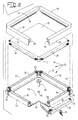
- FIGS 2 and 3 There is shown in Figures 2 and 3 an integrated circuit chip carrier socket 25 for socketing the chip carrier 10.
- the chip carrier 10 in the present example, has relatively short leads 12 projecting outwardly from the edges 28.
- the leads 12 are spaced apart and are substantially flat and straight after being severed from the ring 14 shown in figure 1.
- a substrate or printed circuit board (PCB) 30 is shown having conductive pads 32 arranged in a rectangular pattern on a major surface 34 of the PCB 30.
- the purpose of the socket 25, of the present invention, is to interconnect the lead 12 with respective ones of the pads 32.
- the socket 25 is composed of a body 40, a plurality of contacts 42, and a cover 44.
- a central hole 46 is provided through the body 40 through which a rivet or eyelet 48 is inserted for fastening the socket 25 to the PCB 30 prior to soldering.
- the body 40 includes a bottom 50 and four upstanding walls 52 which form a chip carrier receiving cavity 54 therewithin.
- the bottom 50 and walls 52 are of molded plastic unitary construction.
- a longitudinal groove 56 is formed in each wall 52 as shown in Figures 2 and 4, for a purpose that will be discussed below.
- a plurality of lateral slots 60 are formed through each wall 52 as shown in Figure 2 and are dimensioned to loosely receive the contact 42 therein, as best seen in Figure 4.
- the slots 60 which may be as little as 0.010 of an inch wide to 0.5mm or more, depending on the width of the leads 12, are arranged to leave a bottom web 62 which interconnects the bottom 50 and the remaining portions of the wall 52 for added strength.
- the slots 60 are spaced so that when the socket 25 is properly aligned and attached to the PCB 34 by means of the rivet 48, each slot 60 is directly over a respective one of the pads 32.
- the contact 42 is made of a single piece of flat sheet metal, such as copper alloy for example, having a thickness that is about the same as the width of the leads 12, about 0.010 inch in the present example.
- the contact 42 includes a U-shaped base 64 which is sized to closely slip over the web 62.
- a small protrvsion 66 is formed on one of the inner surfaces of the U-shaped base 64 in a position to engage a hole 68 disposed in the web 62 so that as the contact 42 is inserted into the slot 60 in the direction of the arrow 70 of Figure 2, the U-shaped base snaps firmly into place about the web.
- a terminal 72 extends from one side of the U-shaped base 64 and into engagement with the pad 32 as best seen in Figure 4.
- a pair of openings 74 are provided in the pad engaging surface of the terminal 72 to provide space for solder to accumulate when the terminal is soldered to the pad.
- the contact 42 also includes a tuning fork portion projecting upwardly from the base 64 into the slot 60 which includes a contacting portion 80 and an opposed backup portion 82.
- the contacting portion 80 and backup portion 82 both project from a common bight 84 which is attached to the U-shaped base 64 through a pivotal zone 86.
- the pivotal zone 86 is a relatively narrow section which permits a small amount of pivotal movement of the tuning fork in the directions of the arrows B as shown in Figure 4. The purpose of this pivotal zone 86 will be set forth below.
- the terminal 72 extends outwardly from the wall 52 to permit reflow soldering by a reflow heating tool, focused infrared radiation, hot gas flow, or other such reflow technigues. This also permits optical inspection of the soldered terminal. As set forth above, the openings 74 in the pad engaging surface of the terminal 72 create a condition that is conducive to the formation of solder fillets thereby enabling the soldered interface to be stronger than it would othervise be. Those skilled in the art will appreciate that the terminal 72, instead of being arranged for surface soldering, could be arranged to extend downwardly through a plated through hole, or the like, formed in the PCB 30 in a manner that is well known in the industry.
- the body 40 containing the contacts 42 in the slots 60, is accurately positioned on the surface 34 of the PCB 30 so that the terminals 72 are in alignment with their respective pads 32.
- the rivet or eyelet 48 is then inserted into the hole 46 and through a hole in the PCB 30.
- the rivet or eyelet 48 is peened to provide a downward force on the bottom 50 that slightly deflects the center of the bottom 50 toward the surface 34 of the PCB 30. This downward deflection of the bottom 50 tends to cause all of the terminals 72 to come into engaging contact with their respective pads 32, or at least to come very close thereto. In this way, minor variations in the flatness of the PCB 30 can be tolerated.
- the cover 44 comprises a rectangularly shaped top go being of the approximate shape and dimensions of the body 40 and includes a peripheral shroud 92 projecting downwardly from the four sides of the top 90.
- the top 90 is dimensioned so that the peripheral shroud 92 will slip over the body 40 with minimum clearance between the wall 52 and the shroud 92.
- the top 90 has a clearance opening 94 so that, when assembled to the body 40, as shown in Figure 6, the carrier body 10 may project part way into the opening 94.
- the top 90 includes a locking member 96 which projects downwardly, as viewed in Figure 4, and is spaced from the shroud 92 so that it will be in approximate centering alignment with the slot 56 that runs for substantially the length of the slot. Therefor, when the top 90, chip carrier 10, and base 40 are assembled as shown in Figure 6, the locking member 96 is positioned within its respective slot 56.
- the leads 12 Prior to inserting a chip carrier 10 into the socket 25, the leads 12 are sheared to a specific length leaving them flat and straight. The length of the sheared leads is very short, approximately 1.5mm in the present example.
- the carrier 10 is then placed in the body 40, as best seen in Figure 5, so that all of the leads 12 are loosely positioned within their respective slots 60.
- the cavity 54 and slots 60 are dimensioned so that the cavity 54 loosely aligns the carrier 10 as the carrier enters the cavity thereby aligning the leads 12 with the slots 60. Note that no force is required in placing the carrier into the cavity 54.
- the leads 12 rest on top of the contacting portions 80 and extend toward but are short of the backup portions 82. Note also that the contacting portion 80 and backup portion 82 are substantially centered with the groove 56 which is to provide clearance for the locking member 96.
- the cover 44 With the chip carrier 10 in position within the base 40, the cover 44 is lowered toward the base 44 as indicated by the arrow in Figure 5.
- the inner surface 100 of the shroud 92 engages the walls 52 thereby aligning the locking members 96 with the grooves 56.
- the rounded ends 102 of the locking members 96 engage the leads 12 and begins to deflect them downwardly, bending them about the contacting portions 80 of their respective contacts 42.
- the rounded end 102 is a camming surface which may take the form of an angled surface or other suitable shape. This downward motion continues until the rounded ends 102 engage the bottoms 104 of the slots 56.
- the leads 12 have been bent about 90 degrees downwardly, as viewed in Figure 6, and are pressed against and into electrical contact with their respective contacting portions 80.
- This pressing of the lead 12 against its contacting portion 80 is effected by means of energy stored in the expanded tuning fork which acts in a direction lateral to the bent lead 12.
- the distance between the contacting and backup portions 80 and 82 is less than the combined thickness of the locking number 96 and the lead 12 so that the tuning fork is caused to expand when the cover 44 is assembled as described above. This assures a contact force of about 150 grams between the contacting portion 80 and the lead 12. It is understood that the locking members 96 may not be perfectly straight or all of the contacts 42 in perfect alignment therewith. To accommodate such a condition, the contact will align itself with the locking member 96 as the end 102 begins to bend the lead 12 and engages the backup portion 82, by pivoting in the appropriate direction about the pivotal zone 86 to properly position itself so that the lead 12 is wedged between the contacting member 80 and the locking member 96.
- An important advantage of the present invent ion is the low height which results from this novel structure.
- This low height socket is useful in compact machines such as small lap top computers, ultra thin wall hung display devices or televisions and many other applications having very limited space.
- Another important advantage of the present invention is the relatively short electrical path provided by the socket. The reduction of electrical length enables higher speed switching and provides substantial other related advantages.
- the compact structure of the present invention utilizes a smaller amount of material than would otherwise be required, resulting in lower production costs.
- Another important advantage of the present invention is that a separate step to form the leads in unnecessary resulting in lower manufacturing cost and less chance of damaging the fragile leads. Additionally, since the contact force is supplied by energy stored in the tuning fork structure which acts literally with respect to the leads of the device, no hold down structure is needed as is required by prior art sockets.
Landscapes
- Engineering & Computer Science (AREA)
- Microelectronics & Electronic Packaging (AREA)
- Connecting Device With Holders (AREA)
- Coupling Device And Connection With Printed Circuit (AREA)
- Multi-Conductor Connections (AREA)
Applications Claiming Priority (2)
| Application Number | Priority Date | Filing Date | Title |
|---|---|---|---|
| US07/431,519 US5007845A (en) | 1989-11-03 | 1989-11-03 | Low height chip carrier socket |
| US431519 | 1989-11-03 |
Publications (3)
| Publication Number | Publication Date |
|---|---|
| EP0426349A2 true EP0426349A2 (fr) | 1991-05-08 |
| EP0426349A3 EP0426349A3 (en) | 1992-07-22 |
| EP0426349B1 EP0426349B1 (fr) | 1997-02-12 |
Family
ID=23712294
Family Applications (1)
| Application Number | Title | Priority Date | Filing Date |
|---|---|---|---|
| EP90311546A Expired - Lifetime EP0426349B1 (fr) | 1989-11-03 | 1990-10-22 | Socle support de circuit intégré de faible hauteur |
Country Status (8)
| Country | Link |
|---|---|
| US (1) | US5007845A (fr) |
| EP (1) | EP0426349B1 (fr) |
| JP (1) | JP2550437B2 (fr) |
| KR (1) | KR960014477B1 (fr) |
| CA (1) | CA2027102A1 (fr) |
| DE (1) | DE69029919T2 (fr) |
| ES (1) | ES2097754T3 (fr) |
| IE (1) | IE77635B1 (fr) |
Cited By (1)
| Publication number | Priority date | Publication date | Assignee | Title |
|---|---|---|---|---|
| EP0506263A1 (fr) * | 1991-03-27 | 1992-09-30 | Yamaichi Electronics Co., Ltd. | Connecteur |
Families Citing this family (16)
| Publication number | Priority date | Publication date | Assignee | Title |
|---|---|---|---|---|
| JPH0713191Y2 (ja) * | 1991-02-20 | 1995-03-29 | 日本航空電子工業株式会社 | コネクタ |
| US5192215A (en) * | 1991-10-17 | 1993-03-09 | Amp Incorporated | Electrical socket for leaded chip carriers |
| US5180974A (en) * | 1992-05-26 | 1993-01-19 | Micron Technology, Inc. | Semiconductor testing and shipping system |
| US5295841A (en) * | 1992-10-30 | 1994-03-22 | The Whitaker Corporation | Supportable contact and chip carrier socket for use with an assembly/disassembly tool |
| US5273442A (en) * | 1992-12-24 | 1993-12-28 | The Whitaker Corporation | Modular chip carrier socket |
| US5412540A (en) * | 1993-07-20 | 1995-05-02 | The Whitaker Corporation | Apparatus for removably applying a flat-pack to a socket |
| US5733132A (en) * | 1996-09-30 | 1998-03-31 | Berg Technology, Inc. | Socket for connecting an integrataed circuit to a printed wiring board |
| JP3379897B2 (ja) * | 1997-02-10 | 2003-02-24 | 株式会社日本マイクロニクス | 被検査体試験用補助装置 |
| US6217342B1 (en) | 1997-10-30 | 2001-04-17 | Intercon Systems, Inc. | Interposer assembly |
| US6290507B1 (en) | 1997-10-30 | 2001-09-18 | Intercon Systems, Inc. | Interposer assembly |
| US6315576B1 (en) | 1997-10-30 | 2001-11-13 | Intercon Systems, Inc. | Interposer assembly |
| US20060121754A1 (en) * | 2003-06-13 | 2006-06-08 | Milos Krejcik | Conforming Lid Socket for Leaded Surface Mount Packages |
| JP4720827B2 (ja) * | 2005-07-11 | 2011-07-13 | パナソニック株式会社 | 基板接続部材および接続構造体 |
| TWM285835U (en) * | 2005-07-15 | 2006-01-11 | Top Yang Technology Entpr Co | Chip connector |
| WO2014142246A1 (fr) * | 2013-03-14 | 2014-09-18 | 矢崎総業株式会社 | Structure d'assemblage de composant électronique et boîtier de jonction |
| WO2015029990A1 (fr) * | 2013-08-30 | 2015-03-05 | 矢崎総業株式会社 | Structure de liaison entre composant électronique et accessoire de borne |
Family Cites Families (9)
| Publication number | Priority date | Publication date | Assignee | Title |
|---|---|---|---|---|
| US3391383A (en) * | 1966-06-20 | 1968-07-02 | Hughes Aircraft Co | Electrical connector for integrated circuit elements |
| GB1405417A (en) * | 1971-11-19 | 1975-09-10 | Carr Fastener Co Ltd | Electrical connection sockets |
| US3942854A (en) * | 1974-10-09 | 1976-03-09 | Burroughs Corporation | Hold down device for use in electronic systems employing integrated circuits |
| US4354718A (en) * | 1980-08-18 | 1982-10-19 | Amp Incorporated | Dual-in-line package carrier and socket assembly |
| US4349238A (en) * | 1980-11-05 | 1982-09-14 | Amp Incorporated | Integrated circuit package connector |
| US4527850A (en) * | 1983-11-29 | 1985-07-09 | Sealectro Corp. | Zero insertion force socket |
| JPS6317550A (ja) * | 1986-07-10 | 1988-01-25 | Yamaichi Electric Mfg Co Ltd | Ic載接形ソケツト |
| US4872845A (en) * | 1987-11-03 | 1989-10-10 | Amp Incorporated | Retention means for chip carrier sockets |
| US4869674A (en) * | 1988-05-25 | 1989-09-26 | Pfaff Wayne | Cradle for electronic device package |
-
1989
- 1989-11-03 US US07/431,519 patent/US5007845A/en not_active Expired - Lifetime
-
1990
- 1990-10-03 IE IE354390A patent/IE77635B1/en not_active IP Right Cessation
- 1990-10-05 CA CA002027102A patent/CA2027102A1/fr not_active Abandoned
- 1990-10-22 DE DE69029919T patent/DE69029919T2/de not_active Expired - Fee Related
- 1990-10-22 ES ES90311546T patent/ES2097754T3/es not_active Expired - Lifetime
- 1990-10-22 EP EP90311546A patent/EP0426349B1/fr not_active Expired - Lifetime
- 1990-11-02 KR KR1019900017722A patent/KR960014477B1/ko not_active Expired - Fee Related
- 1990-11-02 JP JP2298762A patent/JP2550437B2/ja not_active Expired - Fee Related
Cited By (1)
| Publication number | Priority date | Publication date | Assignee | Title |
|---|---|---|---|---|
| EP0506263A1 (fr) * | 1991-03-27 | 1992-09-30 | Yamaichi Electronics Co., Ltd. | Connecteur |
Also Published As
| Publication number | Publication date |
|---|---|
| ES2097754T3 (es) | 1997-04-16 |
| US5007845A (en) | 1991-04-16 |
| EP0426349B1 (fr) | 1997-02-12 |
| JP2550437B2 (ja) | 1996-11-06 |
| DE69029919D1 (de) | 1997-03-27 |
| IE77635B1 (en) | 1997-12-31 |
| DE69029919T2 (de) | 1997-08-28 |
| JPH03171577A (ja) | 1991-07-25 |
| EP0426349A3 (en) | 1992-07-22 |
| KR960014477B1 (ko) | 1996-10-15 |
| KR910010671A (ko) | 1991-06-29 |
| IE903543A1 (en) | 1991-05-08 |
| CA2027102A1 (fr) | 1991-05-04 |
Similar Documents
| Publication | Publication Date | Title |
|---|---|---|
| EP0426349B1 (fr) | Socle support de circuit intégré de faible hauteur | |
| AU725875B2 (en) | Low profile connector | |
| US4979903A (en) | Surface mountable contact element and assembly | |
| US4652973A (en) | Chip carrier mounting apparatus | |
| JP3924329B2 (ja) | 多段撓みモードのコネクタと当該コネクタを用いる取り替え可能なチップモジュール | |
| US4410223A (en) | Module mounting assembly | |
| KR20040024458A (ko) | 엘지에이 소케트용 콘택트 | |
| EP0294111B1 (fr) | Connecteur à douille pour les modules ayant des broches d'interconnexion exterieure | |
| KR19990045324A (ko) | 표면 장착 전기 커넥터 | |
| KR100344050B1 (ko) | Pga 패키지용의 낮은 형상 전기 커넥터 및 단자 | |
| US6139348A (en) | Electric connector with an elastically deformable contact pin | |
| EP0303873A2 (fr) | Dispositif de conducteur | |
| US5453700A (en) | Test clip contact arrangement | |
| US6644985B2 (en) | Ball attached zero insertion force socket | |
| EP0047095A2 (fr) | Connecteur pour boîtier électronique sans fils | |
| JPH06302347A (ja) | Icソケット及びそのコンタクト | |
| US5062802A (en) | Contact module for a low height multi-chip carrier socket | |
| US6716060B2 (en) | Electrical connector with solder plate and pegs for PC board mounting | |
| US7413458B2 (en) | Socket for electrical parts | |
| US6485313B1 (en) | BGA socket with improved contacts | |
| EP1091628A2 (fr) | Fassung für elektrische Zwischenverbindung | |
| US20020160643A1 (en) | IC socket and suction-chucking sheet used in the same | |
| EP0578737B1 (fr) | Dispositif de contact pour composant electrique ou electronique | |
| US20240014584A1 (en) | Robust low profile interposer | |
| US6648655B1 (en) | Land grid array socket with supporting members |
Legal Events
| Date | Code | Title | Description |
|---|---|---|---|
| PUAI | Public reference made under article 153(3) epc to a published international application that has entered the european phase |
Free format text: ORIGINAL CODE: 0009012 |
|
| 17P | Request for examination filed |
Effective date: 19901227 |
|
| AK | Designated contracting states |
Kind code of ref document: A2 Designated state(s): DE ES FR GB IT NL SE |
|
| PUAL | Search report despatched |
Free format text: ORIGINAL CODE: 0009013 |
|
| AK | Designated contracting states |
Kind code of ref document: A3 Designated state(s): DE ES FR GB IT NL SE |
|
| RAP1 | Party data changed (applicant data changed or rights of an application transferred) |
Owner name: THE WHITAKER CORPORATION |
|
| 17Q | First examination report despatched |
Effective date: 19940330 |
|
| GRAG | Despatch of communication of intention to grant |
Free format text: ORIGINAL CODE: EPIDOS AGRA |
|
| GRAH | Despatch of communication of intention to grant a patent |
Free format text: ORIGINAL CODE: EPIDOS IGRA |
|
| GRAH | Despatch of communication of intention to grant a patent |
Free format text: ORIGINAL CODE: EPIDOS IGRA |
|
| GRAA | (expected) grant |
Free format text: ORIGINAL CODE: 0009210 |
|
| AK | Designated contracting states |
Kind code of ref document: B1 Designated state(s): DE ES FR GB IT NL SE |
|
| ITF | It: translation for a ep patent filed | ||
| REF | Corresponds to: |
Ref document number: 69029919 Country of ref document: DE Date of ref document: 19970327 |
|
| REG | Reference to a national code |
Ref country code: ES Ref legal event code: FG2A Ref document number: 2097754 Country of ref document: ES Kind code of ref document: T3 |
|
| ET | Fr: translation filed | ||
| PLBE | No opposition filed within time limit |
Free format text: ORIGINAL CODE: 0009261 |
|
| STAA | Information on the status of an ep patent application or granted ep patent |
Free format text: STATUS: NO OPPOSITION FILED WITHIN TIME LIMIT |
|
| 26N | No opposition filed | ||
| PGFP | Annual fee paid to national office [announced via postgrant information from national office to epo] |
Ref country code: NL Payment date: 19980914 Year of fee payment: 9 |
|
| PGFP | Annual fee paid to national office [announced via postgrant information from national office to epo] |
Ref country code: SE Payment date: 19981007 Year of fee payment: 9 |
|
| PGFP | Annual fee paid to national office [announced via postgrant information from national office to epo] |
Ref country code: ES Payment date: 19981021 Year of fee payment: 9 |
|
| PGFP | Annual fee paid to national office [announced via postgrant information from national office to epo] |
Ref country code: FR Payment date: 19991013 Year of fee payment: 10 |
|
| PG25 | Lapsed in a contracting state [announced via postgrant information from national office to epo] |
Ref country code: ES Free format text: LAPSE BECAUSE OF NON-PAYMENT OF DUE FEES Effective date: 19991023 |
|
| PGFP | Annual fee paid to national office [announced via postgrant information from national office to epo] |
Ref country code: DE Payment date: 19991027 Year of fee payment: 10 |
|
| PG25 | Lapsed in a contracting state [announced via postgrant information from national office to epo] |
Ref country code: SE Free format text: THE PATENT HAS BEEN ANNULLED BY A DECISION OF A NATIONAL AUTHORITY Effective date: 19991030 |
|
| PG25 | Lapsed in a contracting state [announced via postgrant information from national office to epo] |
Ref country code: NL Free format text: LAPSE BECAUSE OF NON-PAYMENT OF DUE FEES Effective date: 20000501 |
|
| EUG | Se: european patent has lapsed |
Ref document number: 90311546.7 |
|
| NLV4 | Nl: lapsed or anulled due to non-payment of the annual fee |
Effective date: 20000501 |
|
| PG25 | Lapsed in a contracting state [announced via postgrant information from national office to epo] |
Ref country code: FR Free format text: LAPSE BECAUSE OF NON-PAYMENT OF DUE FEES Effective date: 20010629 |
|
| PG25 | Lapsed in a contracting state [announced via postgrant information from national office to epo] |
Ref country code: DE Free format text: LAPSE BECAUSE OF NON-PAYMENT OF DUE FEES Effective date: 20010703 |
|
| REG | Reference to a national code |
Ref country code: FR Ref legal event code: ST |
|
| REG | Reference to a national code |
Ref country code: GB Ref legal event code: IF02 |
|
| PGFP | Annual fee paid to national office [announced via postgrant information from national office to epo] |
Ref country code: GB Payment date: 20030915 Year of fee payment: 14 |
|
| REG | Reference to a national code |
Ref country code: ES Ref legal event code: FD2A Effective date: 20001113 |
|
| PG25 | Lapsed in a contracting state [announced via postgrant information from national office to epo] |
Ref country code: GB Free format text: LAPSE BECAUSE OF NON-PAYMENT OF DUE FEES Effective date: 20041022 |
|
| GBPC | Gb: european patent ceased through non-payment of renewal fee |
Effective date: 20041022 |
|
| PG25 | Lapsed in a contracting state [announced via postgrant information from national office to epo] |
Ref country code: IT Free format text: LAPSE BECAUSE OF NON-PAYMENT OF DUE FEES;WARNING: LAPSES OF ITALIAN PATENTS WITH EFFECTIVE DATE BEFORE 2007 MAY HAVE OCCURRED AT ANY TIME BEFORE 2007. THE CORRECT EFFECTIVE DATE MAY BE DIFFERENT FROM THE ONE RECORDED. Effective date: 20051022 |