EP0426812B1 - Gallium-arsenid schaltmischstufe - Google Patents
Gallium-arsenid schaltmischstufe Download PDFInfo
- Publication number
- EP0426812B1 EP0426812B1 EP90907888A EP90907888A EP0426812B1 EP 0426812 B1 EP0426812 B1 EP 0426812B1 EP 90907888 A EP90907888 A EP 90907888A EP 90907888 A EP90907888 A EP 90907888A EP 0426812 B1 EP0426812 B1 EP 0426812B1
- Authority
- EP
- European Patent Office
- Prior art keywords
- mixer
- receiving
- transistor
- gallium
- transistors
- Prior art date
- Legal status (The legal status is an assumption and is not a legal conclusion. Google has not performed a legal analysis and makes no representation as to the accuracy of the status listed.)
- Expired - Lifetime
Links
- 229910001218 Gallium arsenide Inorganic materials 0.000 title claims abstract description 25
- JBRZTFJDHDCESZ-UHFFFAOYSA-N AsGa Chemical compound [As]#[Ga] JBRZTFJDHDCESZ-UHFFFAOYSA-N 0.000 title claims description 24
- 238000002347 injection Methods 0.000 claims abstract description 15
- 239000007924 injection Substances 0.000 claims abstract description 15
- 230000008878 coupling Effects 0.000 description 3
- 238000010168 coupling process Methods 0.000 description 3
- 238000005859 coupling reaction Methods 0.000 description 3
- 238000006243 chemical reaction Methods 0.000 description 1
- 230000000295 complement effect Effects 0.000 description 1
- 230000005669 field effect Effects 0.000 description 1
- 238000004804 winding Methods 0.000 description 1
Images
Classifications
-
- H—ELECTRICITY
- H04—ELECTRIC COMMUNICATION TECHNIQUE
- H04H—BROADCAST COMMUNICATION
- H04H40/00—Arrangements specially adapted for receiving broadcast information
Definitions
- This invention relates generally to mixers, and more specifically to gallium-arsenide (GaAs) switching mixers, and is particularly directed toward a GaAs switching mixer employing enhancement mode GaAs switching devices.
- GaAs gallium-arsenide
- GaAs switching mixers have attempted to vary device geometries of GaAs depletion mode devices to minimize the turn-on (switching point) of the devices. While helpful, such variation of depletion mode GaAs devices has not been able to satisfactorily reduce the required local oscillator drive level or harmonic distortion . Accordingly, a need exists for a superior GaAs switching mixer.
- a gallium-arsenide switching mixer for providing an output signal representing the sum and difference frequency, the mixer comprising:
- a GaAs switching mixer receives an information signal and an injection signal to provide an intermediate frequency signal.
- the injection signal controls enhancement mode GaAs devices so as to minimize the required injection drive level and distortion products.
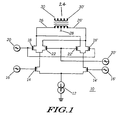
- Figure 1 illustrates a GaAs mixer in accordance with the present invention.
- a switching mixer circuit 10 is arranged in what is commonly known as a double-balanced mixer configuration.
- a current source 12 is coupled from the sources of a differential pair of gallium-arsenide depletion mode field effect transistors 14 and 14' to ground.
- Transistors 14 and 14' are coupled in what is known as a single-balanced configuration.
- the source of transistor 14 is coupled to the source of transistor 14'.
- the drain of transistor 14 is coupled to the sources of a differential pair of enhancement mode gallium-arsenide transistors 18 and 22 and the drain of transistor 14' is coupled to the sources of the differential pair of transistors 18' and 22'.
- Transistors 14 and 14' are as close to being geometrically symmetrical as possible, as are the 18 and 18' transistors and 22 and 22' transistors, respectively.
- the drain of transistor 18 is coupled to a primary terminal 26 of transformer coupling 24 and the drain of transistor 18' is coupled to the opposite primary terminal 26' of transformer coupling 24.
- the drain of transistor 22 is coupled to the drain of transistor 18' and, similarly, the drain of transistor 22' is coupled to the drain transistor 18.
- the primary winding of transformer 24 is center-tapped at terminal 28 to provide a balanced output.
- the secondary coupling of transformer 24 extends between terminals 30 and 30'.
- Radio-frequency information signal 16 is applied to the gate of transistor 14 and radio-frequency signal 16' (i.e., the compliment or negative of signal 16') is applied to the gate of transistor 14'.
- Signals 16 and 16' are known as complementary-phased signals.
- a local oscillator injection signal 20 is applied to the gates of transistors 18 and 18'.
- Signal 20', (the complement of signal 20) is applied to the gates of transistors 22 and 22'.
- the complementary-phased signals 16, 16' cause the source currents in differential pairs 18, 22 and 18', 22' to vary.
- multiplication of complementary-phased signals 16, 16' and complementary-phased signals 20, 20' is accomplished in each of the differential pairs 18, 22 and 18', 22'.
- the output signal appears between terminals 30 and 30'.
Landscapes
- Engineering & Computer Science (AREA)
- Signal Processing (AREA)
- Superheterodyne Receivers (AREA)
- Stabilization Of Oscillater, Synchronisation, Frequency Synthesizers (AREA)
- Transmitters (AREA)
- Medicines Containing Antibodies Or Antigens For Use As Internal Diagnostic Agents (AREA)
- Disintegrating Or Milling (AREA)
Claims (9)
- Eine Gallium-Arsenid Schaltmischeinrichtung (10) zum Bereitstellen eines Ausgangssignals, das die Summen- und Differenzfrequenz darstellt, wobei die Mischeinrichtung umfaßt:eine erste Einrichtung (14, 14') zum Erhalten eines Informationssignals, wobei die genannte erste Einrichtung mindestens einen ersten Transistor (14) umfaßt; undeine zweite Einrichtung (18, 18', 22, 22') zum Erhalten eines Injektionssignals, wobei die genannte zweite Einrichtung mindestens einen zweiten Transistor (18) umfaßt, der mit dem ersten Transistor (14) so gekoppelt ist, daß das Informationssignal und das Injektionssignal kombiniert werden, um das Ausgangssignal zu liefern, wobei die Mischeinrichtung dadurch gekennzeichnet ist, daß der genannte zweite Transistor ein Transistor vom Anreicherungstyp ist, so daß ein verringerter Ansteuerpegel des örtlichen Oszillators und eine verringerte harmonische Verzerrung geschaffen werden.
- Die Mischeinrichtung gemäß Anspruch 1, worin die genannte zweite Einrichtung zum Erhalten eines Injektionssignals mindestens zwei Gallium-Arsenid Transistoren (18, 22) vom Anreicherungstyp einschließt, die in einer Einzelgegentaktausgestaltung gekoppelt sind.
- Die Mischeinrichtung gemäß Anspruch 1, worin die genannte zweite Einrichtung zum Erhalten eines Injektionssignals vier Gallium-Arsenid Transistoren (18, 22, 18', 22') vom Anreicherungstyp einschließt, die in einer Doppelgegentaktausgestaltung gekoppelt sind.
- Die Mischeinrichtung gemäß Anspruch 1, 2 oder 3, worin die erste Einrichtung zum Erhalten eines Injektionssignals ein Paar von Transistoren (14, 14') einschließt.
- Die Mischeinrichtung gemäß Anspruch 1, 2, 3 oder 4, die ferner eine Einrichtung zum Bereitstellen eines abgestimmten Ausgangs (24) umfaßt.
- Die Mischeinrichtung gemäß Anspruch 1, 2, 3, 4 oder 5, worin die erste Einrichtung zum Erhalten eines Informationssignals ein Paar Transistoren (14, 14') vom Verarmungstyp einschließt.
- Die Mischeinrichtung gemäß Anspruch 6, worin die erste Einrichtung zum Erhalten eines Informationssignals ein Paar Gallium-Arsenid Transistoren (14, 14') vom Verarmungstyp einschließt.
- Die Mischeinrichtung gemäß Anspruch 1, 2, 3, 4 oder 5, worin die erste Einrichtung zum Erhalten eines Informationssignals ein Paar Transistoren vom Anreicherungstyp einschließt.
- Die Mischeinrichtung gemäß Anspruch 8, worin die erste Einrichtung zum Erhalten eines Informationssignals ein Paar Gallium-Arsenid Transistoren vom Anreicherungstyp einschließt.
Applications Claiming Priority (3)
| Application Number | Priority Date | Filing Date | Title |
|---|---|---|---|
| US34526989A | 1989-05-01 | 1989-05-01 | |
| US345269 | 1989-05-01 | ||
| PCT/US1990/002284 WO1990014150A2 (en) | 1989-05-01 | 1990-04-25 | Gallium-arsenide switching mixer |
Publications (3)
| Publication Number | Publication Date |
|---|---|
| EP0426812A1 EP0426812A1 (de) | 1991-05-15 |
| EP0426812A4 EP0426812A4 (en) | 1992-01-15 |
| EP0426812B1 true EP0426812B1 (de) | 1996-08-28 |
Family
ID=23354299
Family Applications (1)
| Application Number | Title | Priority Date | Filing Date |
|---|---|---|---|
| EP90907888A Expired - Lifetime EP0426812B1 (de) | 1989-05-01 | 1990-04-25 | Gallium-arsenid schaltmischstufe |
Country Status (7)
| Country | Link |
|---|---|
| EP (1) | EP0426812B1 (de) |
| JP (1) | JPH03506110A (de) |
| AT (1) | ATE142058T1 (de) |
| DE (1) | DE69028275T2 (de) |
| DK (1) | DK0426812T3 (de) |
| ES (1) | ES2090133T3 (de) |
| WO (1) | WO1990014150A2 (de) |
Citations (1)
| Publication number | Priority date | Publication date | Assignee | Title |
|---|---|---|---|---|
| GB2177860A (en) * | 1985-07-09 | 1987-01-28 | Multitone Electronics Plc | R.F. mixer |
Family Cites Families (3)
| Publication number | Priority date | Publication date | Assignee | Title |
|---|---|---|---|---|
| US4603435A (en) * | 1984-08-20 | 1986-07-29 | Gte Laboratories Incorporated | Microwave mixer apparatus |
| DE3509327A1 (de) * | 1985-03-15 | 1986-09-25 | Telefunken electronic GmbH, 7100 Heilbronn | Dynamischer frequenzteiler mit mischstufe und verstaerker |
| US4896374A (en) * | 1988-12-09 | 1990-01-23 | Siemens Aktiengesellschaft | Broadband monolithic balanced mixer apparatus |
-
1990
- 1990-04-25 EP EP90907888A patent/EP0426812B1/de not_active Expired - Lifetime
- 1990-04-25 DE DE69028275T patent/DE69028275T2/de not_active Expired - Fee Related
- 1990-04-25 WO PCT/US1990/002284 patent/WO1990014150A2/en not_active Ceased
- 1990-04-25 JP JP2507253A patent/JPH03506110A/ja active Pending
- 1990-04-25 DK DK90907888.3T patent/DK0426812T3/da active
- 1990-04-25 AT AT90907888T patent/ATE142058T1/de not_active IP Right Cessation
- 1990-04-25 ES ES90907888T patent/ES2090133T3/es not_active Expired - Lifetime
Patent Citations (1)
| Publication number | Priority date | Publication date | Assignee | Title |
|---|---|---|---|---|
| GB2177860A (en) * | 1985-07-09 | 1987-01-28 | Multitone Electronics Plc | R.F. mixer |
Also Published As
| Publication number | Publication date |
|---|---|
| EP0426812A4 (en) | 1992-01-15 |
| WO1990014150A2 (en) | 1990-11-29 |
| DK0426812T3 (da) | 1996-09-16 |
| DE69028275T2 (de) | 1997-03-13 |
| JPH03506110A (ja) | 1991-12-26 |
| EP0426812A1 (de) | 1991-05-15 |
| ES2090133T3 (es) | 1996-10-16 |
| WO1990014150A3 (en) | 1991-04-04 |
| DE69028275D1 (de) | 1996-10-02 |
| ATE142058T1 (de) | 1996-09-15 |
Similar Documents
| Publication | Publication Date | Title |
|---|---|---|
| US5752181A (en) | Method and apparatus for reducing inermodulation distortion in a mixer | |
| EP0854568B1 (de) | Monolithische integrierte Mikrowellenschaltung | |
| US6871059B1 (en) | Passive balun FET mixer | |
| US6064872A (en) | Totem pole mixer having grounded serially connected stacked FET pair | |
| US4682061A (en) | MOSFET transistor switch control | |
| US5551076A (en) | Circuit and method of series biasing a single-ended mixer | |
| EP0131337A1 (de) | Doppelgegentakt-Mischer | |
| JPH09153781A (ja) | スイッチ回路 | |
| US10141888B2 (en) | Double balanced mixer | |
| US20030052727A1 (en) | High linearity, high gain mixer circuit | |
| US4949398A (en) | GaAs MESFET balanced resistive mixer | |
| KR19990008262A (ko) | 보상 링 믹서 | |
| US5732345A (en) | Quasi-double balanced dual-transformer dual FET mixer, which achieves better isolation by using a first and second diplexer, and a transmission line RF balun | |
| US5323123A (en) | Integrated circuit having a variable-gain amplifier | |
| US20030157918A1 (en) | Double balanced FET mixer with high IP3 and IF response down to DC levels | |
| US4403156A (en) | Frequency conversion circuit | |
| US6861891B2 (en) | Sub-harmonic mixer | |
| KR880000366Y1 (ko) | 밸런스드 믹서회로 | |
| US5732344A (en) | Additive HF mixer | |
| WO1990014150A2 (en) | Gallium-arsenide switching mixer | |
| CA1199378A (en) | High frequency amplifier with phase compensation | |
| US20040106391A1 (en) | Sub-harmonic mixer | |
| JPH0629811A (ja) | Fetスイッチ | |
| KR100407841B1 (ko) | 불평형전계효과트랜지스터믹서 | |
| JP2563286B2 (ja) | 周波数混合回路 |
Legal Events
| Date | Code | Title | Description |
|---|---|---|---|
| PUAI | Public reference made under article 153(3) epc to a published international application that has entered the european phase |
Free format text: ORIGINAL CODE: 0009012 |
|
| 17P | Request for examination filed |
Effective date: 19901217 |
|
| AK | Designated contracting states |
Kind code of ref document: A1 Designated state(s): AT BE CH DE DK ES FR GB IT LI LU NL SE |
|
| D17D | Deferred search report published (deleted) | ||
| A4 | Supplementary search report drawn up and despatched |
Effective date: 19911128 |
|
| AK | Designated contracting states |
Kind code of ref document: A4 Designated state(s): AT BE CH DE DK ES FR GB IT LI LU NL SE |
|
| 17Q | First examination report despatched |
Effective date: 19940711 |
|
| GRAH | Despatch of communication of intention to grant a patent |
Free format text: ORIGINAL CODE: EPIDOS IGRA |
|
| GRAH | Despatch of communication of intention to grant a patent |
Free format text: ORIGINAL CODE: EPIDOS IGRA |
|
| GRAA | (expected) grant |
Free format text: ORIGINAL CODE: 0009210 |
|
| AK | Designated contracting states |
Kind code of ref document: B1 Designated state(s): AT BE CH DE DK ES FR GB IT LI LU NL SE |
|
| REF | Corresponds to: |
Ref document number: 142058 Country of ref document: AT Date of ref document: 19960915 Kind code of ref document: T |
|
| REG | Reference to a national code |
Ref country code: CH Ref legal event code: NV Representative=s name: JOHN P. MUNZINGER INGENIEUR-CONSEIL |
|
| ITF | It: translation for a ep patent filed | ||
| REG | Reference to a national code |
Ref country code: DK Ref legal event code: T3 |
|
| ET | Fr: translation filed | ||
| REF | Corresponds to: |
Ref document number: 69028275 Country of ref document: DE Date of ref document: 19961002 |
|
| REG | Reference to a national code |
Ref country code: ES Ref legal event code: FG2A Ref document number: 2090133 Country of ref document: ES Kind code of ref document: T3 |
|
| REG | Reference to a national code |
Ref country code: ES Ref legal event code: FG2A Ref document number: 2090133 Country of ref document: ES Kind code of ref document: T3 |
|
| PG25 | Lapsed in a contracting state [announced via postgrant information from national office to epo] |
Ref country code: SE Effective date: 19961128 |
|
| PGFP | Annual fee paid to national office [announced via postgrant information from national office to epo] |
Ref country code: AT Payment date: 19970417 Year of fee payment: 8 |
|
| PLBE | No opposition filed within time limit |
Free format text: ORIGINAL CODE: 0009261 |
|
| STAA | Information on the status of an ep patent application or granted ep patent |
Free format text: STATUS: NO OPPOSITION FILED WITHIN TIME LIMIT |
|
| 26N | No opposition filed | ||
| PGFP | Annual fee paid to national office [announced via postgrant information from national office to epo] |
Ref country code: GB Payment date: 19980401 Year of fee payment: 9 |
|
| PGFP | Annual fee paid to national office [announced via postgrant information from national office to epo] |
Ref country code: FR Payment date: 19980407 Year of fee payment: 9 |
|
| PGFP | Annual fee paid to national office [announced via postgrant information from national office to epo] |
Ref country code: DK Payment date: 19980414 Year of fee payment: 9 |
|
| PGFP | Annual fee paid to national office [announced via postgrant information from national office to epo] |
Ref country code: NL Payment date: 19980420 Year of fee payment: 9 |
|
| PGFP | Annual fee paid to national office [announced via postgrant information from national office to epo] |
Ref country code: CH Payment date: 19980422 Year of fee payment: 9 |
|
| PGFP | Annual fee paid to national office [announced via postgrant information from national office to epo] |
Ref country code: ES Payment date: 19980423 Year of fee payment: 9 Ref country code: DE Payment date: 19980423 Year of fee payment: 9 |
|
| PG25 | Lapsed in a contracting state [announced via postgrant information from national office to epo] |
Ref country code: AT Free format text: LAPSE BECAUSE OF NON-PAYMENT OF DUE FEES Effective date: 19980425 |
|
| PGFP | Annual fee paid to national office [announced via postgrant information from national office to epo] |
Ref country code: BE Payment date: 19980428 Year of fee payment: 9 |
|
| PGFP | Annual fee paid to national office [announced via postgrant information from national office to epo] |
Ref country code: LU Payment date: 19980821 Year of fee payment: 9 |
|
| PG25 | Lapsed in a contracting state [announced via postgrant information from national office to epo] |
Ref country code: LU Free format text: LAPSE BECAUSE OF NON-PAYMENT OF DUE FEES Effective date: 19990425 Ref country code: GB Free format text: LAPSE BECAUSE OF NON-PAYMENT OF DUE FEES Effective date: 19990425 |
|
| PG25 | Lapsed in a contracting state [announced via postgrant information from national office to epo] |
Ref country code: ES Free format text: LAPSE BECAUSE OF NON-PAYMENT OF DUE FEES Effective date: 19990426 |
|
| PG25 | Lapsed in a contracting state [announced via postgrant information from national office to epo] |
Ref country code: LI Free format text: LAPSE BECAUSE OF NON-PAYMENT OF DUE FEES Effective date: 19990430 Ref country code: DK Free format text: LAPSE BECAUSE OF NON-PAYMENT OF DUE FEES Effective date: 19990430 Ref country code: CH Free format text: LAPSE BECAUSE OF NON-PAYMENT OF DUE FEES Effective date: 19990430 Ref country code: BE Free format text: LAPSE BECAUSE OF NON-PAYMENT OF DUE FEES Effective date: 19990430 |
|
| BERE | Be: lapsed |
Owner name: MOTOROLA INC. Effective date: 19990430 |
|
| PG25 | Lapsed in a contracting state [announced via postgrant information from national office to epo] |
Ref country code: NL Free format text: LAPSE BECAUSE OF NON-PAYMENT OF DUE FEES Effective date: 19991101 |
|
| GBPC | Gb: european patent ceased through non-payment of renewal fee |
Effective date: 19990425 |
|
| REG | Reference to a national code |
Ref country code: CH Ref legal event code: PL |
|
| PG25 | Lapsed in a contracting state [announced via postgrant information from national office to epo] |
Ref country code: FR Free format text: LAPSE BECAUSE OF NON-PAYMENT OF DUE FEES Effective date: 19991231 |
|
| NLV4 | Nl: lapsed or anulled due to non-payment of the annual fee |
Effective date: 19991101 |
|
| REG | Reference to a national code |
Ref country code: FR Ref legal event code: ST |
|
| PG25 | Lapsed in a contracting state [announced via postgrant information from national office to epo] |
Ref country code: DE Free format text: LAPSE BECAUSE OF NON-PAYMENT OF DUE FEES Effective date: 20000201 |
|
| REG | Reference to a national code |
Ref country code: DK Ref legal event code: EBP |
|
| REG | Reference to a national code |
Ref country code: ES Ref legal event code: FD2A Effective date: 20010503 |
|
| PG25 | Lapsed in a contracting state [announced via postgrant information from national office to epo] |
Ref country code: IT Free format text: LAPSE BECAUSE OF NON-PAYMENT OF DUE FEES;WARNING: LAPSES OF ITALIAN PATENTS WITH EFFECTIVE DATE BEFORE 2007 MAY HAVE OCCURRED AT ANY TIME BEFORE 2007. THE CORRECT EFFECTIVE DATE MAY BE DIFFERENT FROM THE ONE RECORDED. Effective date: 20050425 |