EP0427228A2 - Système de réglage de la valeur de seuil dans un circuit récepteur - Google Patents
Système de réglage de la valeur de seuil dans un circuit récepteur Download PDFInfo
- Publication number
- EP0427228A2 EP0427228A2 EP90121301A EP90121301A EP0427228A2 EP 0427228 A2 EP0427228 A2 EP 0427228A2 EP 90121301 A EP90121301 A EP 90121301A EP 90121301 A EP90121301 A EP 90121301A EP 0427228 A2 EP0427228 A2 EP 0427228A2
- Authority
- EP
- European Patent Office
- Prior art keywords
- threshold value
- constant
- signal
- variable
- mode setting
- Prior art date
- Legal status (The legal status is an assumption and is not a legal conclusion. Google has not performed a legal analysis and makes no representation as to the accuracy of the status listed.)
- Granted
Links
Images


Classifications
-
- H—ELECTRICITY
- H04—ELECTRIC COMMUNICATION TECHNIQUE
- H04L—TRANSMISSION OF DIGITAL INFORMATION, e.g. TELEGRAPHIC COMMUNICATION
- H04L25/00—Baseband systems
- H04L25/02—Details ; arrangements for supplying electrical power along data transmission lines
- H04L25/06—DC level restoring means; Bias distortion correction ; Decision circuits providing symbol by symbol detection
- H04L25/061—DC level restoring means; Bias distortion correction ; Decision circuits providing symbol by symbol detection providing hard decisions only; arrangements for tracking or suppressing unwanted low frequency components, e.g. removal of DC offset
- H04L25/065—Binary decisions
-
- H—ELECTRICITY
- H04—ELECTRIC COMMUNICATION TECHNIQUE
- H04L—TRANSMISSION OF DIGITAL INFORMATION, e.g. TELEGRAPHIC COMMUNICATION
- H04L25/00—Baseband systems
- H04L25/02—Details ; arrangements for supplying electrical power along data transmission lines
- H04L25/06—DC level restoring means; Bias distortion correction ; Decision circuits providing symbol by symbol detection
- H04L25/061—DC level restoring means; Bias distortion correction ; Decision circuits providing symbol by symbol detection providing hard decisions only; arrangements for tracking or suppressing unwanted low frequency components, e.g. removal of DC offset
- H04L25/062—Setting decision thresholds using feedforward techniques only
Definitions
- the present invention relates to a threshold value control system in a receiver circuit in an ISDN (Integrated Systems Digital Network) terminal or in a network termination in an ISDN network.
- ISDN Integrated Systems Digital Network
- Japanese Patent Publication No. 61-227440 is known to the public.
- a comparator is conventionally used for comparing an input signal and a threshold voltage so as to discriminate the digital signal level of the input signal.
- the methods for determining the threshold voltage conventionally, there are a fixed method in which the threshold voltage is constant and an ATC (Automatic Threshold Control) method in which the threshold voltage is approximately linearly changed dependent on the voltage of the input signal.
- an object of the present invention is, based on the idea of adding a NT/TE switching function, in the ATC system, to prevent bit errors or synchronization deviation in the receiver circuit due to the fluctuation of the digital signals when determining threshold value by the influence of noises, or due to the fluctuation of digital signals when determining threshold values by the superimposition of frame synchronization signals when a plurality of ISDN terminals are connected to a network termination by a bus.
- a threshold value control system for discriminating an input signal received by a receiver circuit.
- the system comprises a mode setting unit for determining a mode setting signal.
- the mode corresponds to a connection pattern by which the receiver circuit is connected to another terminal.
- the system further comprises a variable threshold value generating unit for generating a variable threshold value which varies depending on the variation of the level of the input signal; a constant threshold value generating unit for generating at least one constant threshold value by which the level of the input signal can be discriminated even when the level of the input signal cannot be distinguished by the variable threshold value; a threshold comparing unit for comparing the variable threshold value and each of the at least one constant threshold values to output a comparison result; a switching unit for passing only one of the variable threshold values and the at least one constant threshold value as an input digital signal discriminating threshold value, based on the mode setting signal output from the mode setting unit and the comparison result output from the threshold comparing unit.
- the input digital signal discriminating threshold value is, as a result, sufficient to discriminate the digital level of the input signal.
- the system still further comprises a comparing unit for comparing the level of the input signal and the input digital signal discriminating threshold value to output a discriminated result.
- the receiver circuit is included in, for example, one of the NT1, NT2, and ISDN terminals in an ISDN network.
- the model setting unit comprises a unit for generating an NT mode selecting signal when the receiver circuit is included in a terminal acting as a network termination in an ISDN network, and comprises a unit for generating a TE mode selecting signal when the receiver circuit is included in a terminal acting as terminal equipment in an ISDN network.
- the variable threshold value generating unit comprises a unit for generating the variable threshold value which is a predetermined percentage of the peak level of the input signal and which increases in accordance with an increase in the level of the input signal.
- the constant threshold value generating unit comprises a threshold value comparing unit for comparing the variable threshold value with each of the at least one constant threshold values to generate a comparison result, and further comprises a switch control unit for generating a switch control signal based on the mode setting signal output from the mode setting unit and the comparison result output from the threshold comparing unit.
- the input digital signal discriminating threshold value is output from the switching unit in response to the switch control signal output from the switch control unit.
- the constant threshold value generating unit comprises a first threshold voltage generating unit for generating a first constant threshold value by which the input digital signal level can be discriminated by the comparing unit even when the variable threshold value is increased to be higher than the first constant threshold value so that the input digital signal level cannot be discriminated by the increased variable threshold value due to superimposition of frame signals from a plurality of terminals, and the switching unit comprises a unit for outputting the first threshold value when the variable threshold value is higher than the first constant threshold value and when the mode setting unit generates the NT mode selecting signal.
- the switching unit comprises a unit for outputting the variable threshold value when the variable threshold value is lower than or equal to the first constant threshold value and higher than or equal to the second constant threshold value, and when the mode setting unit generates the NT mode selecting signal.
- the switching unit comprises a unit for outputting the second threshold value when the variable threshold value is lower than the second constant threshold value and when the mode setting unit generates the NT mode selecting signal.
- the switching unit comprises a unit for outputting the variable threshold value when the variable threshold value is higher than or equal to the second constant threshold value and when the mode setting unit generates the TE mode selecting signal.
- the switching unit comprises a unit for outputting the second threshold value when the variable threshold value is lower than the second constant threshold value and when the mode setting unit generates the TE mode selecting signal.
- the switching unit comprises a unit for outputting the variable threshold value when the variable threshold value is lower than or equal to the first constant threshold value and higher than or equal to the second constant threshold value, and when the mode setting unit generates the NT mode selecting signal; a unit for outputting the second constnat threshold value when the variable threshold value is lower than the second constant threshold value and when the mode setting unit generates the NT mode selecting signal; a unit for outputting the variable threshold value when the variable threshold value is higher than or equal to the second constnat threshold value and when the mode setting unit generates the TE mode selecting signal; and a unit for outputting the second constant threshold value when the variable threshold value is lower than the second constant threshold value and when the mode setting unit generates the TE mode selecting signal.
- FIG. 1 is a block diagram showing an example of the construction of an ISDN network, for explaining the field of utilization in industry of the present invention.
- an ISDN exchange 41 is connected through a U-reference point to a network termination (NT1) 42, and the network termination (NT1) 42 is connected through a T-reference point to a network termination (NT2) 43, or is directly connected through a S/T reference point and not through the network termination (NT2) 43 to a maximum of eight ISDN terminals (TE) 44.
- TE ISDN terminals
- the (NT1) 42 has, as illustrated in the figure, the functions of terminating at a subscriber line, maintenance, monitoring, and timing functions in the layer 1, etc.
- the (NT2) 43 has functions such as protocol processing in the layers 2 and 3 and exchange function of a PBX, LAN and so forth.
- the (TE) 44 is a digital telephone set and so forth having the functions of protocol processing, maintenance functions, interface functions and so forth.
- the present invention relates to the receiver circuit in the network termination (NT1) 42 or (NT2) 43, or in the ISDN terminals (TE) 44.
- FIG. 2 is a block diagram showing the construction of the ISDN terminal (TE) 44 as background of the present invention.
- a voice signal from a hand set 51 is converted into a B-channel digital signal by a coder/decoder (CODEC) 52.
- Control signals stored in a ROM and RAM are read out under the control of a central processing unit (CPU) 53.
- a frame decomposing/composing circuit (F D/C) 54 composes a frame of 2B + D. This frame is transmitted to the S-reference point and the T-reference point through a driver 55 and pulse transformer 56.
- a comparator and so forth is used to detect the digital input waveform of the input from the line side (S/T reference point) to output a signal to the frame decomposing/composing circuit (F D/C) 54 wherein it is synchronized with the signal on the line, or the frame is decomposed into B1, B2, and D channels and is transmitted as a receiving signal into the internal circuit.
- F D/C frame decomposing/composing circuit
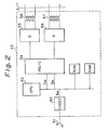
- FIG. 3 is a block diagram 2 showing an ISDN network system including receiver circuits.
- a driver circuit (D) 31 in a network termination (NT1) 32 is connected through a pulse transformer to a receiver circuit (R) 33 in a network termination (NT2) 34.
- a driver circuit (D) 35 in the network termination (NT2) 34 is connected through a pulse transformer to a receiver circuit (R) 36 in an ISDN terminal 37.
- the network termination (NT2) 34 includes a receiver circuit (R) 38
- the network termination (NT1) 32 includes a receiver circuit (R) 39.
- the present invention relates to threshold voltage for detecting signals input to these receiver circuits.
- the threshold voltages are constant, and an ATC (Automatic Threshold Control) method in which the threshold voltage is approximately linearly changed dependent on the peak voltage of the input signal.
- Figure 4 is a graph explaining the conventional fixed method. In the figure, it is depicted that the voltage of the input waveform is lowered in accordance with the increase of the line loss. In this way, the input signal level differs depending on the line length between the network termination (NT2) 43 and the other terminal.
- NT2 network termination
- the amount of signal delay may change or the distortion of the waveform may change.
- connection patterns e.g., the cases where only one ISDN terminal (TE) 44 is connected to the network termination (NT2) 44 by a point-to-point connection, where all of the eight ISDN terminals (TE) 44 are positioned at places far from the network termination (NT2) 43 for more than 200 meters and are connected by a multi-point connection, and where only one of the eight terminals is placed to close to the network termination and the remaining seven terminals are placed at a remote location.
- the distortion of the waveform or the amount of signal delay may change depending on whether the format of the signal input to the receiver circuit is a continuous pulse format or a signal pulse format.
- the pulse width or the delay time of the signal transmitted to the internal circuit of the receiver circuit may change.
- the interval between the signal changing point of the output signal of an ISDN standard terminal (TE) and the signal changing point of the corresponding signal applied to the input of the ISDN standard terminal (TE) should not exceed the range between -7% and +15% of the bit period.
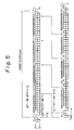
- Figure 5 is a diagram showing a conventional frame construction at the user-network interface reference point S/T.
- the frame construction of the signal transmitted in the direction from the NT1 or NT2 to the TE is shown in the upper portion
- the frame construction of the signal output from the TE to the NT1 or N12 for establishing the frame synchronization in response to the signal in the upper portion is shown in the lower portion.
- Framing bits in both signals should be separated in time by a 2-bit offset.
- Figure 6 is a diagram showing the framing-bit portion extracted and expanded from both signals in Fig. 5.
- the time difference between a zero-cross point P1 of the frame pulse in the input signal into the receiver circuit in the terminal equipment (TE) and a zero-cross point P2 of the frame pulse in the output signal from the driver circuit in the same terminal equipment (TE) as above is 10.42 ⁇ s which is double the 5.21 ⁇ s of the pulse width of one bit. Accordingly, the total phase deviation is within the regulation range between -7% and *15% of the pulse width of 5.21 ⁇ s.
- the level of the signal, the waveform distortion, or the delay amount may fluctuate dependent on the change of the line length, connection pattern, and signal format as described before. Because of this fluctuation, it is difficult to satisfy the regulation of the total phase deviation when the receiving signal is detected by a signal threshold voltage according to the conventional fixed method. Therefore, as shown in Fig. 4, it may be considered to provide a plurality of threshold voltages V TH1 , ..., V THn-1 , and V THn .
- the ATC Automatic Threshold Control
- a peak value of the waveform on the line is detected, the peak value of the signal is held, and the voltage corresponding to the peak held value is used as a threshold voltage.
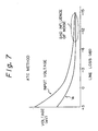
- Fig. 7 is a graph showing the change of the threshold voltage utilizing the ATC method. As shown in the figure, the input voltage of the receiving signal is lowered according to the increase of the line loss, and the threshold voltage is also lowered according to the decrease of the input voltage.
- the threshold voltage is determined to be, for example, about 50% of the input voltage.
- the threshold voltage is approximately linearly change in accordance with the change of the input waveform voltage, the regulation of the total phase deviation is easily satisfied in comparison with the fixed method.
- the line loss is increased in accordance with the elongation of the distance between the network termination (NT2) 43 and the network termination (NT1) 42 or the single ISDN terminal (TE) 44.
- the signal level is lowered so that the noise level is close to the signal level. In this situation, noises and so forth are held at peak instead of holding the peak value of the signal level.
- the threshold voltage is determined in accordance with the peak held value of the noises and so forth, the correct detection of the signal cannot be carried out so that the problems of bit errors and synchronization deviation easily occur.
- the distance between terminals in the point-to-point connection should be limited to be shorter than a constant in comparison with the fixed method.
- the eight ISDN terminals (TE) 44 are connected by a bus at the S reference point of the network termination (NT2) 43 shown in Fig. 1.
- the receiver circuit connected to the network termination (NT1) 42 is operated in a TE mode of the point-to-point connection
- the receiver circuit connected to the ISDN terminal (TE) 44 is operated in an NT mode of the multi-point connection.
- the eight ISDN terminals (TE) 44 always transmit frame synchronization signals even when signals of the B channel and the D channel are not transmitted.
- the frame synchronization signals from a plurality of ISDN terminals (TE) 44 are superimposed at the S reference point, the level of the frame synchronization signal becomes higher than the signal level of the B channel or the D channel.
- the elevated synchronization signal is explained in more detail with reference to Figs. 8A and 8B. Namely, as shown in Fig. 8A, in the TE mode operation or even in the NT mode operation in case of the point-to-point connection, the height of the frame synchronization signal and the height of the B channel signal or the D channel signal are all the same. Note that the signals shown in Figs. 8A and 8B are AMI codes. In contrast, as shown in Fig.
- the high level of the frame synchronization signal becomes higher than the high level of the B channel signal or the D channel signal, and the low level of the frame synchronization signal becomes lower than the low level of the B channel signal or the D channel signal.
- the conventional ATC method when the conventional ATC method is applied, the elevated level of the frame synchronization signal is held as peak, and the threshold value is determined in accordance with the peak held value. Therefore, the threshold value is too high to detect the input signal of the B channel or the D channel so that the digital signal level cannot be correctly determined.
- the NT mode receiver circuit As a countermeasure to the increase of the threshold voltage due to the superimposition of the frame synchronization signals, it may be considered to have different threshold voltages in the NT mode receiver circuit and the TE mode receiver circuit.
- the network termination (NT2) 43 two kinds of evaluation tests should be effected so that the evaluation tests become complicated. Further, since the receiver circuits having different characteristics should be constructed by different circuits having different characteristics, the cost becomes high.
- an object of the present invention is, based on the idea of adding a NT/TE switching function, in the ATC system, to prevent bit errors or synchronization deviation in the receiver circuit due to the fluctuation of the digital signal determining threshold value by the influence of noises, or due to the fluctuation of digital signal determining threshold value by the superimposition of frame signals when a plurality of ISDN terminals are connected to a network termination by a bus.
- FIG. 9 is a principal block diagram of a receiver circuit in an ISDN terminal or a network termination according to an embodiment of the present invention.
- 1 is a peak voltage holding unit (PHU) for holding the peak voltage value of an input signal
- 2 is an automatic threshold value control unit (ATC) for outputting a variable threshold value Va which varies according to the peak voltage value held in the peak voltage holding unit 1
- 3 is a comparing unit (COMP) for comparing the voltage value of the input signal and the variable threshold value Va which is output from the automatic threshold control unit 2, to discriminate the digital signal level of the input signal
- 4 is a constant threshold generating unit (V REF ) for outputting a constant threshold value V1 by which the digital signal level of the input signal can be discriminated even when the digital signal level of the input signal cannot be discriminated by an increased variable threshold value Va which has been increased in accordance with the increase of the input signal voltage.
- V REF constant threshold generating unit
- the automatic threshold control unit 2 outputs the variable threshold value Va when the variable threshold value Va is equal to or smaller than the constant threshold value V1 output from the constant threshold generating unit 4, and outputs the constant threshold value V1 output from the constant threshold generating unit 4 when the variable threshold value Va is larger than the above-mentioned constant threshold value V1.
- the constant threshold generating unit 4 outputs a first constant threshold value V1 by which the digital signal level of the input signal can be discriminated even when the digital signal level V IN of the input signal cannot be discriminated by an increased variable threshold value Va which has been increased in accordance with the increase of the input signal voltage V IN , and outputs a second constant threshold value V2 by which the digital level of the input signal can be discriminated even when the influence of the noise level on the variable threshold value Va can not be neglected in accordance with the decrease of the voltage of the input signal.
- the automatic threshold control unit 2 has a mode setting terminal 5 for switching between an NT mode used in the case of bus connection and a TE mode used in the case of point-to-point connection.
- the automatic threshold control unit 2 outputs the variable threshold value Va to the comparing unit 3 when the variable threshold value Va is equal to or lower than the first constant threshold value V1, and outputs the first constant threshold value V1 output from the constant threshold generating unit 4 to the comparing unit 3 when the variable threshold value Va is higher than the first constant threshold V1.
- the automatic threshold control unit 2 When the TE mode is set at the mode setting terminal 5, the automatic threshold control unit 2 outputs the variable threshold value Va even when the variable threshold value Va is higher than the first constant threshold value V1. In the case of either the NT mode setting time or the TE mode setting time, the automatic threshold control unit 2 outputs the second constant threshold value V2 output from the constant threshold generating unit 4 when the variable threshold value Va is smaller than the second constant threshold value V2.
- the eight ISDN terminals (TE) 44 may be located at a far-end position or at a near-end position with respect to the network termination (NT1) 42 or (NT2) 43.
- the signal levels at the input of the network termination are different because the distance between the ISDN terminals is relatively long. Even when the signal levels are different, however, it is sufficient for detecting each signal level to determine the first constant threshold value V1 and the second constant threshold value V2 to be smaller than the lowest signal level.
- the constant threshold value V1 when the variable threshold value Va is higher than the constant threshold value V1, output from the constant threshold generating unit 4, the constant threshold value V1 output form the constant threshold generating unit 4 is output to the comparing unit 3, and thereby, in the ATC method, even when the frame synchronization signals from a plurality of terminals are superimposed in the case of the multipoint connection, the threshold voltage is fixed to the constant threshold value V1 so that the bit errors or the synchronization deviations can be prevented.
- the second aspect of the present invention by switching the mode setting in accordance with the location of the usage of the receiver circuit, the fluctuation of the threshold voltage due to noises in the case of the point-to-point connection can be prevented, and thereby bit errors or synchronization errors can be prevented.
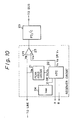
- FIG. 10 is a block diagram showing the construction of a receiver circuit in an ISDN terminal or a network termination, according to an embodiment of the present invention.
- 21 is a peak hold circuit for holding the peak voltage value of the input signal
- 22 is an ATC circuit for outputting a variable threshold value Va which varies in accordance with the peak voltage value
- 23 is a comparator for comparing the voltage value V IN of the input signal and the output of the ATC circuit 22 to determine the digital signal level of the input signal
- 24 is a constant threshold generating circuit for outputting a constant threshold value V1 by which the digital signal level of the input signal can be recognized even when the digital signal level of the input signal cannot be discriminated by the variable threshold value Va because the variable threshold value has been increased to be too high in accordance with the increase of the input signal voltage V IN .
- the constant threshold generating circuit 24 also generates a second constant threshold value V2 by which the digital signal level of the input signal can be discriminated even when the digital signal level of the input signal cannot be discriminated by the variable threshold value Va which has been decreased to be too low so that so that the negative influence of noises cannot be neglected.
- the ATC circuit 22 By setting the terminal A and B either manually or under the control by the CPU, the ATC circuit 22 is set in an NT mode or in a TE mode in which the receiver circuit is used.
- the ATC circuit 22 When the receiver circuit is to be connected to an ISDN terminal (TE) by a bus, the ATC circuit 22 is set to the NT mode.
- the ATC circuit 22 When the receiver circuit is to be connected to the network termination (NT1) or (NT2) by a point-to-point connection, the ATC circuit 22 is set to the TE mode.
- the mode setting is realized by inputting a setting signal to the mode setting terminals A and B.
- the mode settings other than the NT mode and the TE mode, it is also possible to set the conventional fixed system, ATC system, externally input mode, and so forth. In the illustrated example, since there are two setting terminals, four different mode settings are possible. If it is desired to further increrase the number of the setting modes, the number of setting terminals may be increased.
- Fiugure 11 is a graph illustrating the relation between the input waveform voltage and the threshold voltage, for explaining the operation of the circuit shown in Fig. 10.
- the constant threshold forming circuit 24 outputs the first constant threshold value V1 by which the gigital signal level of the input isgnal can be discriminated. Also, even when the influence of the noise level in the input signal on the variable threshold value Va cannot be neglected in accordance with the decrease of the input signal voltage V IN , the second constant threshold value V2 by which the digital signal level V IN of the input signal can be discriminated is output.
- the ATC circuti 22 When the NT mode is being set, the ATC circuti 22 outputs to the comparator 23, when the variable threshold value Va is below the first constant threshold value V1, the variable threshold value Va which varies in response to the change of the input voltage in accordance with the conventional ATC methos. When the variable threshold value Va exceeds the first constant threshold value V1, the first constant threshold value V1 output from the constant threshold generating circuit 24 is output from the ATC circuit 22 to the comparator 23. Namely, at the time of setting the NT mode, by the operation of the ATC circuit 22, three stages are switched among the fixed method when the line loss is small, the ATC method in the next step, and then the fixed method when the line loss becomes larger.
- the ATC circuit 22 When the TE mode is being set, the ATC circuit 22 outputs the variable threshold value Va even when the variable threshold value Va is higher than the first constant threshold value V1. Namely, in the TE mode, when the input signal voltage V IN is high, the conventional ATC method is employed; and when the line loss becomes large, the fixed method is employed in the same way as the NT mode setting time.
- the ATC circuit 22 outputs the second constant threshold value V2 output from the constant threshold generating circuit 24 when the variable threshold value Va is smaller than the second constant threshold value V2.
- the ATC method and the fixed method are combined so that when the variable threshold voltage Va by the ATC method is lower than V2, it is switched to the fixed system, so that noises and so forth do not ifluence on the threshold voltage even when the line length is elongated.
- the fixed threshold level V2 should be sufficiently high so that noise waveforms are not detected when there is no signal on the line.
- the digital level V IN of the input signal cannot be discriminated by the variable threshold value Va due to the superimposition of the frame signals at the time of bus connection and due to the higher level of the frame synchronization signal hgiher than the B or D channel signal.
- the threshold voltage is fixed to V1 so that the above-mentioned problem is resolved.
- the discriminated level of the input signal compared with the digital signal discriminating threshold value by the comparator 25 is output to the frame decomposition/composition circuit 25 in the layer 1.
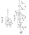
- Figure 12 is a circuit diagram showing an example of the constant threshold forming circuit 24 shown in Fig. 10.
- the constant threshold generating circuit 24 is constructed by resistors (R1 and R2) 121 and 122, a capacitor (C1) 123, and an operational amplifier (OP1) 124.
- the resistors 121 and 122 are connected in series between the power supply line V DD and ground.
- the connecting point between the resistors 121 and 122 is connected to the noninverting input of the operational amplifier 124.
- the capacitor 123 is connected between the noninverting input of the operational amplifier 124 and ground.
- the output of the operational amplifier 124 is connected to the inverting input thereof.
- FIG. 13 is a circuit diagram showing an example of the peak hold circuit 21 shown in Fig. 10.
- the peak hold circuit 21 is constructed by two operational amplifiers (OP2 and OP3) 131 and 132, a resistor (R3) 133 connected between the inverting input of the operational amplifier 131 and ground, a diode (D1) 134 for conducting a positive current, a resistor (R4) 135 and a capacitor (C2) 236 constituting an integrating circuit for holding the peak voltage of the input signal applied to the noninverting input of the operational amplifier 131, resistors (R5 and R6) 137 and 138 for amplifying the voltage applied to the noninverting input of the operational amplifier 132, a capacitor (C3) 139 connected between the output of the operational amplifier 132 and ground, and resistors (R7 and R8) 140 and 141 connected in series between the output of the operational amplifier 132 and ground.
- an output voltage which is held at the peak value of the input signal is
- FIG 14 is a block diagram showing an example of the ATC circuit 22 shown in Fig. 10.
- the ATC circuit 22 is constructed by a selector circuit (SEL) 142, a switch control circuit (SW CONT) 143, two constant threshold generating circuits 144 and 145, two comparators (COMP1 and COMP2) 146 and 147, and three switches (SW1, SW2 and SW3) 148, 149 and 150.
- the constitution of each of the constant threshold generating circuits 144 and 145 is substantially the same as shown in Fig. 12, where the constant threshold value V1 or V2 is determined by the ratio of the resistances R1 and R2.
- the selector circuit 142 In operation of the ATC circuit, the selector circuit 142 outputs a 3-bit selecting signal in response to a 2-bit mode setting signal applied to setting terminals A and B.
- the constant threshold generating circuit 144 outputs the first constant threshold value V1
- the constant threshold generating circuit 145 outputs the second constant threshold value V2,.
- the comparator 146 outputs a high level signal when the variable threshold value Va is higher than the first constant threshold value V1, and outputs a low level signal when the variable threshold value Va is lower than the first constant threshold value V1.
- the comparator 147 outputs a high level signal when the variable threshold value Va is higher than the second constant rhreshold value V2, and outputs a low level signal when the variable threshold value Va is lower than the second constant threshold value V2.
- the switch control circuit 143 selects one of the three outputs 1, 2 and 3 to be energized. In response to the energized output signal 1, 2 or 3, the corresponding switch 148, 149 or 150 is turned on to output on ATC output signal. Namely, when the set mode is the NT mode, only the switch 149 is turned ON to output the V1 as the ATC output signal when Va is larger than V1; only the switch 148 is turned ON to output the Va as the ATC output signal when Va is smaller than V1 and higher than V2; and only the switch 150 is turned ON to output the V2 as the ATC output signal when Va is lower than V2. Similarly, when the set mode is the TE mode, only the switch 148 is turned ON to output Va when Va is higher than V2; and only the switch 150 is turned ON when Va is lower than V2.
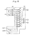
- Figure 15 is a circuit diagram showing an example of the construction of the selector circuit 142 and the switch control circuit 143 shown in Fig. 14.
- the selector circuit 142 is constructed by inverters 151 and 152, and NAND gates 153, 154, and 155 forming a decoder.
- the switch control circuit 143 is constructed by inverters 156 and 157, and NAND gates 158 to 169, forming an another decoder.
- a receiver circuit in an ISDN terminal or in a network temrination since the influence of noises on the line on the treshold voltage is removed, and in the NT mode, since the negative influence of the superimposed waves of frame synchronization signals on the signal detection is removed, bit errors or synchronization deviation due to these influences can be prevented. Also, by providing the switching function between the NT mode and the TE mode, circuits having the same characteristic can be commonly used for either the NT mode or the TE mode so that the cost is lower in comparison with the case when the circuits are manufactured with different characteristics for the NT mode and the TE mode.
Landscapes
- Engineering & Computer Science (AREA)
- Power Engineering (AREA)
- Computer Networks & Wireless Communication (AREA)
- Signal Processing (AREA)
- Dc Digital Transmission (AREA)
- Manipulation Of Pulses (AREA)
- Synchronisation In Digital Transmission Systems (AREA)
Applications Claiming Priority (2)
| Application Number | Priority Date | Filing Date | Title |
|---|---|---|---|
| JP291066/89 | 1989-11-10 | ||
| JP1291066A JPH0828750B2 (ja) | 1989-11-10 | 1989-11-10 | レシーバ回路における自動閾値制御方式 |
Publications (3)
| Publication Number | Publication Date |
|---|---|
| EP0427228A2 true EP0427228A2 (fr) | 1991-05-15 |
| EP0427228A3 EP0427228A3 (fr) | 1992-12-30 |
| EP0427228B1 EP0427228B1 (fr) | 1998-04-01 |
Family
ID=17763981
Family Applications (1)
| Application Number | Title | Priority Date | Filing Date |
|---|---|---|---|
| EP90121301A Expired - Lifetime EP0427228B1 (fr) | 1989-11-10 | 1990-11-07 | Système de réglage de la valeur de seuil dans un circuit récepteur |
Country Status (5)
| Country | Link |
|---|---|
| US (1) | US5091920A (fr) |
| EP (1) | EP0427228B1 (fr) |
| JP (1) | JPH0828750B2 (fr) |
| CA (1) | CA2029108C (fr) |
| DE (1) | DE69032195T2 (fr) |
Cited By (4)
| Publication number | Priority date | Publication date | Assignee | Title |
|---|---|---|---|---|
| EP0635954A3 (fr) * | 1993-07-20 | 1997-12-17 | Hitachi, Ltd. | Circuit d'attaque et de réception pour transmission en duplex intégral |
| EP0659312A4 (fr) * | 1993-06-16 | 1999-08-04 | Universal Data Systems Inc | Egaliseur a retour de decision, appareil et procede d'utilisation. |
| EP0829987A3 (fr) * | 1996-09-12 | 2000-04-12 | Nec Corporation | Etablissement des seuils de décision dans des récepteurs MDFM |
| EP0997902A3 (fr) * | 1998-10-28 | 2002-04-24 | Victor Company of Japan, Ltd. | Appareil de contrôle de fréquence et appareil de reproduction de signal numérique |
Families Citing this family (17)
| Publication number | Priority date | Publication date | Assignee | Title |
|---|---|---|---|---|
| US5546419A (en) * | 1991-01-29 | 1996-08-13 | Siemens Aktiengesellschuft | Bus coupler |
| EP0649582A4 (fr) * | 1992-06-30 | 1997-10-08 | Heuer H Instr Pty Ltd | Appareil de test d'ecarts pour reseaux digitaux de services integres. |
| US5475342A (en) * | 1993-04-19 | 1995-12-12 | Nippon Telegraph And Telephone Corporation | Amplifier for stably maintaining a constant output |
| US5691959A (en) * | 1994-04-06 | 1997-11-25 | Fujitsu, Ltd. | Stylus position digitizer using acoustic waves |
| US5459762A (en) * | 1994-09-16 | 1995-10-17 | Rockwell International Corporation | Variable multi-threshold detection for 0.3-GMSK |
| JP4291410B2 (ja) * | 1994-12-09 | 2009-07-08 | ブレント タウンシェンド、 | 高速データ転送エンコーダ、デコーダ、システム、エンコード方法および復号方法 |
| US5970103A (en) | 1996-09-06 | 1999-10-19 | Townshend; Brent | High speed communications system for analog subscriber connections |
| US5815507A (en) * | 1996-04-15 | 1998-09-29 | Motorola, Inc. | Error detector circuit for digital receiver using variable threshold based on signal quality |
| JPH10173456A (ja) * | 1996-12-11 | 1998-06-26 | Fujitsu Ltd | 信号増幅回路 |
| US6879645B1 (en) * | 1998-09-15 | 2005-04-12 | Tut Systems, Inc. | Method and apparatus for dynamically varying the noise sensitivity of a receiver |
| US6879644B1 (en) * | 1998-09-15 | 2005-04-12 | Tut Systems, Inc. | Method and apparatus for automatically determining a peak voltage level for a data signal propagated on a carrier medium |
| JP3504176B2 (ja) * | 1998-12-02 | 2004-03-08 | 富士通株式会社 | 信号増幅回路 |
| JP3674753B2 (ja) * | 1999-03-09 | 2005-07-20 | 富士通株式会社 | バースト信号検出回路 |
| US6493336B1 (en) * | 1999-03-30 | 2002-12-10 | Nortel Networks Limited | System optimized always on dynamic integrated services digital network |
| US8094591B1 (en) * | 2002-03-19 | 2012-01-10 | Good Technology, Inc. | Data carrier detector for a packet-switched communication network |
| US7711071B2 (en) * | 2002-07-31 | 2010-05-04 | Nxp B.V. | Setting the slice level in a binary signal |
| US7483986B2 (en) * | 2003-12-03 | 2009-01-27 | International Business Machines Corporation | Dynamically tuning networks of relationships in self-organizing multi-agent systems |
Family Cites Families (7)
| Publication number | Priority date | Publication date | Assignee | Title |
|---|---|---|---|---|
| US4091379A (en) * | 1976-05-03 | 1978-05-23 | Litton Business Systems, Inc. | Analog to digital wave shaping system |
| JPS6012826B2 (ja) * | 1980-01-07 | 1985-04-03 | 株式会社日立製作所 | 受信回路 |
| US4414512A (en) * | 1981-05-29 | 1983-11-08 | Motorola Inc. | Broadband peak detector |
| JPS61227440A (ja) * | 1985-04-02 | 1986-10-09 | Fujitsu Ltd | 網終端装置のクロツク選択制御装置 |
| US4879727A (en) * | 1986-09-05 | 1989-11-07 | Advanced Micro Devices Inc. | Adaptive threshold sampling controller |
| US4965795A (en) * | 1988-05-10 | 1990-10-23 | Harris Corporation | D channel monitor |
| US4926442A (en) * | 1988-06-17 | 1990-05-15 | International Business Machines Corporation | CMOS signal threshold detector |
-
1989
- 1989-11-10 JP JP1291066A patent/JPH0828750B2/ja not_active Expired - Fee Related
-
1990
- 1990-10-31 US US07/607,033 patent/US5091920A/en not_active Expired - Lifetime
- 1990-11-01 CA CA002029108A patent/CA2029108C/fr not_active Expired - Fee Related
- 1990-11-07 DE DE69032195T patent/DE69032195T2/de not_active Expired - Fee Related
- 1990-11-07 EP EP90121301A patent/EP0427228B1/fr not_active Expired - Lifetime
Cited By (5)
| Publication number | Priority date | Publication date | Assignee | Title |
|---|---|---|---|---|
| EP0659312A4 (fr) * | 1993-06-16 | 1999-08-04 | Universal Data Systems Inc | Egaliseur a retour de decision, appareil et procede d'utilisation. |
| EP0635954A3 (fr) * | 1993-07-20 | 1997-12-17 | Hitachi, Ltd. | Circuit d'attaque et de réception pour transmission en duplex intégral |
| EP0829987A3 (fr) * | 1996-09-12 | 2000-04-12 | Nec Corporation | Etablissement des seuils de décision dans des récepteurs MDFM |
| EP0997902A3 (fr) * | 1998-10-28 | 2002-04-24 | Victor Company of Japan, Ltd. | Appareil de contrôle de fréquence et appareil de reproduction de signal numérique |
| US6768706B1 (en) | 1998-10-28 | 2004-07-27 | Victor Company Of Japan, Ltd | Frequency control apparatus and digital signal reproducing apparatus |
Also Published As
| Publication number | Publication date |
|---|---|
| US5091920A (en) | 1992-02-25 |
| JPH03153144A (ja) | 1991-07-01 |
| DE69032195T2 (de) | 1998-09-03 |
| EP0427228B1 (fr) | 1998-04-01 |
| JPH0828750B2 (ja) | 1996-03-21 |
| CA2029108C (fr) | 1995-09-26 |
| EP0427228A3 (fr) | 1992-12-30 |
| DE69032195D1 (de) | 1998-05-07 |
| CA2029108A1 (fr) | 1991-05-11 |
Similar Documents
| Publication | Publication Date | Title |
|---|---|---|
| EP0427228A2 (fr) | Système de réglage de la valeur de seuil dans un circuit récepteur | |
| EP0734012B1 (fr) | Circuit de discrimination de signal | |
| KR100325674B1 (ko) | 식별회로 | |
| JPH04506731A (ja) | ビット誤り率検出 | |
| US5933458A (en) | Circuit for processing asynchronous signals having periodic synchronization bursts | |
| US5050190A (en) | Signal detection circuit not affected by minute voltage fluctuations contained in input signal and operation method therefor | |
| US6151691A (en) | Remote reporting system for digital transmission line elements | |
| US5218635A (en) | Low-frequency alternating current signal detector, in particular for central office line interface circuits | |
| EP0138693A1 (fr) | Méthode et appareil pour surveiller une ligne de transmission radio digitale | |
| US7626399B2 (en) | Broken lead detection | |
| US5999593A (en) | System and method for automatic PBX detection | |
| US6556673B1 (en) | Telephone ring signal detector | |
| JP2000349605A (ja) | 識別回路 | |
| EP0344751A2 (fr) | Circuit de détection des violations de code utilisé en transmission d'un signal AMI | |
| EP1049304A1 (fr) | Systeme d'essai de controle de canal | |
| JP3064168B2 (ja) | プログラマブルコントローラ | |
| US5777494A (en) | Signal discrimination circuit for unknown signal amplitude and distortion | |
| DE102004009745B4 (de) | Empfängerschaltung für APM-kodierte Daten | |
| CA2122180C (fr) | Circuit de commande d'affaiblissement automatique | |
| KR100282440B1 (ko) | 잡음 억제 회로 | |
| US4833692A (en) | Non-linear amplifier for digital network | |
| US7116256B1 (en) | Pulse shaping apparatus and method | |
| EP0217607A2 (fr) | Circuit de réglage de la valeur de seuil pour une interface à signal vidéo et appareil d'enregistrement équipé de celui-ci | |
| GB2341992A (en) | Voltage polarity reversal detector with hysteresis | |
| JPH0215748A (ja) | ディジタル伝送装置評価方式 |
Legal Events
| Date | Code | Title | Description |
|---|---|---|---|
| PUAI | Public reference made under article 153(3) epc to a published international application that has entered the european phase |
Free format text: ORIGINAL CODE: 0009012 |
|
| AK | Designated contracting states |
Kind code of ref document: A2 Designated state(s): DE FR GB |
|
| PUAL | Search report despatched |
Free format text: ORIGINAL CODE: 0009013 |
|
| AK | Designated contracting states |
Kind code of ref document: A3 Designated state(s): DE FR GB |
|
| 17P | Request for examination filed |
Effective date: 19930121 |
|
| 17Q | First examination report despatched |
Effective date: 19960108 |
|
| GRAG | Despatch of communication of intention to grant |
Free format text: ORIGINAL CODE: EPIDOS AGRA |
|
| GRAG | Despatch of communication of intention to grant |
Free format text: ORIGINAL CODE: EPIDOS AGRA |
|
| GRAH | Despatch of communication of intention to grant a patent |
Free format text: ORIGINAL CODE: EPIDOS IGRA |
|
| GRAH | Despatch of communication of intention to grant a patent |
Free format text: ORIGINAL CODE: EPIDOS IGRA |
|
| GRAA | (expected) grant |
Free format text: ORIGINAL CODE: 0009210 |
|
| AK | Designated contracting states |
Kind code of ref document: B1 Designated state(s): DE FR GB |
|
| REF | Corresponds to: |
Ref document number: 69032195 Country of ref document: DE Date of ref document: 19980507 |
|
| ET | Fr: translation filed | ||
| PLBE | No opposition filed within time limit |
Free format text: ORIGINAL CODE: 0009261 |
|
| STAA | Information on the status of an ep patent application or granted ep patent |
Free format text: STATUS: NO OPPOSITION FILED WITHIN TIME LIMIT |
|
| 26N | No opposition filed | ||
| REG | Reference to a national code |
Ref country code: GB Ref legal event code: IF02 |
|
| PGFP | Annual fee paid to national office [announced via postgrant information from national office to epo] |
Ref country code: GB Payment date: 20031105 Year of fee payment: 14 |
|
| PGFP | Annual fee paid to national office [announced via postgrant information from national office to epo] |
Ref country code: FR Payment date: 20031110 Year of fee payment: 14 |
|
| PGFP | Annual fee paid to national office [announced via postgrant information from national office to epo] |
Ref country code: DE Payment date: 20031120 Year of fee payment: 14 |
|
| PG25 | Lapsed in a contracting state [announced via postgrant information from national office to epo] |
Ref country code: GB Free format text: LAPSE BECAUSE OF NON-PAYMENT OF DUE FEES Effective date: 20041107 |
|
| PG25 | Lapsed in a contracting state [announced via postgrant information from national office to epo] |
Ref country code: DE Free format text: LAPSE BECAUSE OF NON-PAYMENT OF DUE FEES Effective date: 20050601 |
|
| GBPC | Gb: european patent ceased through non-payment of renewal fee |
Effective date: 20041107 |
|
| PG25 | Lapsed in a contracting state [announced via postgrant information from national office to epo] |
Ref country code: FR Free format text: LAPSE BECAUSE OF NON-PAYMENT OF DUE FEES Effective date: 20050729 |
|
| REG | Reference to a national code |
Ref country code: FR Ref legal event code: ST |