EP0427254B1 - Verfahren zum Herstellen einer Kontaktzone - Google Patents
Verfahren zum Herstellen einer Kontaktzone Download PDFInfo
- Publication number
- EP0427254B1 EP0427254B1 EP90121381A EP90121381A EP0427254B1 EP 0427254 B1 EP0427254 B1 EP 0427254B1 EP 90121381 A EP90121381 A EP 90121381A EP 90121381 A EP90121381 A EP 90121381A EP 0427254 B1 EP0427254 B1 EP 0427254B1
- Authority
- EP
- European Patent Office
- Prior art keywords
- layer
- tungsten
- forming
- contact
- semiconductor
- Prior art date
- Legal status (The legal status is an assumption and is not a legal conclusion. Google has not performed a legal analysis and makes no representation as to the accuracy of the status listed.)
- Expired - Lifetime
Links
Images

Classifications
-
- H—ELECTRICITY
- H10—SEMICONDUCTOR DEVICES; ELECTRIC SOLID-STATE DEVICES NOT OTHERWISE PROVIDED FOR
- H10W—GENERIC PACKAGES, INTERCONNECTIONS, CONNECTORS OR OTHER CONSTRUCTIONAL DETAILS OF DEVICES COVERED BY CLASS H10
- H10W20/00—Interconnections in chips, wafers or substrates
- H10W20/01—Manufacture or treatment
- H10W20/031—Manufacture or treatment of conductive parts of the interconnections
- H10W20/056—Manufacture or treatment of conductive parts of the interconnections by filling conductive material into holes, grooves or trenches
- H10W20/057—Manufacture or treatment of conductive parts of the interconnections by filling conductive material into holes, grooves or trenches by selectively depositing, e.g. by using selective CVD or plating
-
- H—ELECTRICITY
- H10—SEMICONDUCTOR DEVICES; ELECTRIC SOLID-STATE DEVICES NOT OTHERWISE PROVIDED FOR
- H10D—INORGANIC ELECTRIC SEMICONDUCTOR DEVICES
- H10D64/00—Electrodes of devices having potential barriers
- H10D64/01—Manufacture or treatment
- H10D64/011—Manufacture or treatment of electrodes ohmically coupled to a semiconductor
- H10D64/0111—Manufacture or treatment of electrodes ohmically coupled to a semiconductor to Group IV semiconductors
- H10D64/0112—Manufacture or treatment of electrodes ohmically coupled to a semiconductor to Group IV semiconductors using conductive layers comprising silicides
-
- H—ELECTRICITY
- H10—SEMICONDUCTOR DEVICES; ELECTRIC SOLID-STATE DEVICES NOT OTHERWISE PROVIDED FOR
- H10W—GENERIC PACKAGES, INTERCONNECTIONS, CONNECTORS OR OTHER CONSTRUCTIONAL DETAILS OF DEVICES COVERED BY CLASS H10
- H10W20/00—Interconnections in chips, wafers or substrates
- H10W20/01—Manufacture or treatment
- H10W20/031—Manufacture or treatment of conductive parts of the interconnections
- H10W20/032—Manufacture or treatment of conductive parts of the interconnections of conductive barrier, adhesion or liner layers
- H10W20/033—Manufacture or treatment of conductive parts of the interconnections of conductive barrier, adhesion or liner layers in openings in dielectrics
-
- H—ELECTRICITY
- H10—SEMICONDUCTOR DEVICES; ELECTRIC SOLID-STATE DEVICES NOT OTHERWISE PROVIDED FOR
- H10W—GENERIC PACKAGES, INTERCONNECTIONS, CONNECTORS OR OTHER CONSTRUCTIONAL DETAILS OF DEVICES COVERED BY CLASS H10
- H10W20/00—Interconnections in chips, wafers or substrates
- H10W20/01—Manufacture or treatment
- H10W20/071—Manufacture or treatment of dielectric parts thereof
- H10W20/081—Manufacture or treatment of dielectric parts thereof by forming openings in the dielectric parts
-
- H—ELECTRICITY
- H10—SEMICONDUCTOR DEVICES; ELECTRIC SOLID-STATE DEVICES NOT OTHERWISE PROVIDED FOR
- H10P—GENERIC PROCESSES OR APPARATUS FOR THE MANUFACTURE OR TREATMENT OF DEVICES COVERED BY CLASS H10
- H10P14/00—Formation of materials, e.g. in the shape of layers or pillars
- H10P14/60—Formation of materials, e.g. in the shape of layers or pillars of insulating materials
- H10P14/69—Inorganic materials
- H10P14/692—Inorganic materials composed of oxides, glassy oxides or oxide-based glasses
- H10P14/6921—Inorganic materials composed of oxides, glassy oxides or oxide-based glasses containing silicon
- H10P14/69215—Inorganic materials composed of oxides, glassy oxides or oxide-based glasses containing silicon the material being a silicon oxide, e.g. SiO2
Definitions
- the present invention relates to a method for forming contact regions in a semiconductor device having an active element and/or passive element formed in a semiconductor substrate comprising silicon, and more particularly to such a method for forming contact regions which allows the formation of a wiring or interconnection layer of good quality even in a contact hole of a greater aspect ratio.
- Al-Si and Al-Si-Cu alloys For a very small metal wiring or interconnection layer for LSI's, use has been made of aluminum, or aluminum alloys such as Al-Si and Al-Si-Cu alloys. These aluminum-based materials are usually deposited by sputtering so as to form interconnection layers. If, however, an Al-based layer is formed by such a sputtering in a contact hole of a greater aspect ratio (that is, a ratio of the depth to the width of the opening of the contact hole), more Al-based material is deposited on the upper inner edge of the contact hole to provide a thickened portion. The presence of such a thickened portion causes a "shadowing" phenomenon, producing a lowering of a step coverage at the Al-based layer. As a result, the Al-based material is thinly deposited in the inner edge of the contact hole and, in a worst case, a breakage occurs in the Al-based material layer at the bottom corner of the contact hole.
- a conductive material is embedded on the bottom of the contact hole if the contact hole has a greater aspect ratio. By so doing, the aspect ratio is substantially lowered in actual practice.
- One approach to this problem is to deposit tungsten by a chemical vapor deposition (CVD) method in the contact hole over the semiconductor substrate. Tungsten is usually deposited there through a vapor phase reaction of a tungsten halide (feed gas) with a reducing agent such as hydrogen or silane.
- CVD chemical vapor deposition
- contact holes involves forming an insulating layer by a thermal oxidation on the surface of a semiconductor silicon substrate having predetermined semiconductor regions formed in the surface portion thereof. Then contact holes are formed in the insulating layer, by a photolithography method, partially exposing the semiconductor regions. Then an impurity of a given concentration is introduced in a relatively high impurity level in the exposed surface portion of the substrate at those areas of the contact holes to provide impurity areas for taking an ohmic contact.
- the tungsten layer as deposited in the contact hole usually reveals a feeble bond to the underlying semiconductor silicon substrate.
- a native oxide film readily tends to be formed on the surface of the P + region in particular. The presence of the native oxide film has a greater tendency for the tungsten layer's bond to be weakened and, as a result, the resultant semiconductor device manifests a degradation in its properties, such as an increased electrical resistance at the contact region.
- the property of the tungsten layer largely depends upon the type of impurity, its concentration level or its surface state in the underlying semiconductor silicon substrate.
- IBM Technical Disclosure Bulletin, Vol. 30, No. 8, Jan 1988, p343-344 shows forming a silicide layer as a protective barrier for the silicon substrate during RIE etching.
- a thin layer of tungsten is formed by sputtering to improve the reliability of an AlCuSi conductor.
- IEDM technical digest CH-1973-7, 1983, p. 550-553 shows refilling contact windows or via holes with tungsten by selective CVD employing WF 6 , at a temperature of 350°C.
- WF 6 selective CVD
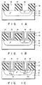
- a P type impurity such as BF 2
- a P type impurity is selectively ion-implanted into a predetermined area of an N type silicon substrate 11 at a dose of 5 ⁇ 10 15 cm -2 .
- the resultant structure is heat treated at a temperature of about 800°C to provide a P + impurity region 12 of a predetermined diffusion depth.
- the impurity concentration of the P + impurity region 12 is set in a range of, for example, 5 ⁇ 10 19 /cm 3 .
- N type impurity such as an As
- An N type impurity is selectively ion-implanted in a predetermined portion of the P + impurity region 12 at a dose of 5 ⁇ 10 15 cm -2 .
- the resultant structure is heat treated at a temperature of about 800°C to provide an N + impurity region 13.
- the impurity concentration of the N + impurity region 13 is set at about 10 20 /cm 3 .
- An insulating layer is formed on a major surface of the substrate 13 including the surfaces of the P + impurity region 12 and N + impurity region 13.
- the insulating layer is formed of, for example, SiO 2 .
- contact holes 15 and 16 are formed by a photolithography method in the insulating layer to partially expose the surfaces of the P + impurity region 12 and N + impurity region 13.
- the remaining insulating layer 14 protects PN junction parts which would otherwise be exposed on the major surface of the semiconductor substrate 11.
- a transition metal such as titanium
- a sputtering such as a magnetron sputtering
- a titanium layer 17 is formed on the surface of the aforementioned structure.
- use may be made of other transition metals, such as nickel (Ni), cobalt (Co), tungsten (W).
- the transition metal layer can also be formed by a plating method.
- the nitride layer 18 preferably has a thickness of 500 to 1500 ⁇ .
- the titanium nitride layer 18 serves to make uniform a thickness of silicide layers 19 and 20 (Fig. 1C) to be formed through a reaction (silicidation) as will be set out below.
- resultant structure (Fig. 1B) is heat treated for 0.5 to 1.0 hours at a temperature of 600 to 700°C to conduct a reaction (silicidation) of the titanium in the titanium layer 17 with the substrate silicon.
- a reaction sicidation
- titanium silicide layers 19 and 20 are formed beneath the bottoms 15a and 16a of the contact holes 15 and 16.
- those areas around the silicide layers 19 and 20 cause no substantial thickening of other areas owing to the presence of the titanium nitride layer 18, so that the silicide layers 19 and 20 are made to have a substantial uniform thickness as a whole.
- the transition metal layer conducts no reaction with the insulating layer SiO 2 .
- the arsenic (As) in the impurity region 13 has an effect of suppressing the aforementioned silicidation reaction. For this reason, the silicide layer 19 in the P + impurity region 12 is thickened relative to the silicide layer 20 in the N + impurity region 13.
- the titanium layer 17 and titanium nitride layer 18, including those remaining on the side walls 15b and 16b of the contact holes 15 and 16, are selectively removed by an etchant, such as sulfuric acid, through their dissolution.
- an etchant such as sulfuric acid
- a mixed gas of a tungsten halide and a reducing agent is supplied over the resultant structure heated to a predetermined temperature, and tungsten layers 21, growing tungsten layers 21 and 22, as shown in Fig. 1E, on the titanium silicide layers 19 and 20 at the contact holes 15 and 16.
- a tungsten halide use can be made of a tungsten hexafluoride gas (WF 6 ).
- WF 6 tungsten hexafluoride gas
- a reducing agent use can be made of a hydrogen gas, silane (SiH 4 ) gas. In this Embodiment, a mixture of SiH 4 and WF 6 gases was used and, in this case, the heating temperature of the silicon substrate structure is preferably in a range of 300 to 400°C.
- the SiH 4 /WF 6 gas flow ratio is 1.0 or less in the formation of the tungsten layers 21 and 22, these layers are selectively grown in the contact holes 15 and 16 only. If, on the other hand, the SiH 4 /WF 6 gas flow ratio exceeds 1.0, the tungsten layer is grown in the contact holes 15 and 16 and also on the whole surface of the insulating layer 14. The whole surface of the tungsten layer can be selectively removed by an etch-back step to leave the tungsten layer as a buried layer only at the interior of the contact holes and 16.
- a wiring or interconnection layer of aluminum or aluminum alloy such as an Al-Si or Al-Si-Cu alloy, are formed by an ordinary process to connect with the corresponding contact regions comprising the tungsten layers 15 and 16, providing a semiconductor device.
- the silicide layers 19 and 20 are formed prior to the formation of the tungsten layers. It is thus possible to prevent a tungsten encroachment which has been encountered when a tungsten layer is formed directly on the semiconductor silicon substrate structure.
- the silicide layers 19 and 20 provide a strong bond to the tungsten layers 21 and 22 and reveal a better shape integrity.
- the tungsten layers 21 and 22 of a better quality can be provided over the semiconductor substrate structure without being influenced by the type and concentration level of an impurity in the semiconductor silicon substrate (underlying layer structure).
- the resistance of the contact regions of a tungsten layer buried in contact holes of 1 ⁇ m was as small as 50 to 60 ⁇ according to the present invention, a value very much smaller than 1000 ⁇ for a conventional case where a tungsten layer is formed directly on the substrate through a hydrogen reduction of WF 6 .
- a leakage current is of the order of 10 -10 to 10 -11 A for the contact region formed according to the present invention and of the order of 10 -7 to 10 -8 A for the conventional contact region.
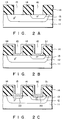
- an impurity region 12 and an impurity region 13 are formed at predetermined locations in the semiconductor silicon substrate 11 as in Embodiment 1.
- an insulating layer 14 is formed on a major surface of the semiconductor substrate 11 to cover the impurity region 12 and impurity impurity 13, as in Embodiment 1.
- Contact holes 15 and 16 are formed in the insulating layer 14 to expose the impurity regions 12 and 13, as in Embodiment 1.
- a titanium layer 31 is formed by a magnetron sputtering on the insulating layer 14 and in contact holes 15 and 16 of the silicon substrate 11, as shown in Fig. 2B.
- the titanium layer 31 preferably has a thickness of 500 to 1500 ⁇ .
- a uniform plasma is generated, by a magnetron sputtering, between the target titanium and the silicon substrate under a magnetic field by the magnetron, thus achieving a uniformity in a ratio of an amount of titanium deposited per unit area in the sputtering step and a thickness uniformity of the titanium layer 31.
- the semiconductor structure as shown in Fig. 2B is heat treated, for example, for 0.5 to 1.0 hours at a temperature of 600 to 700°C in a nitrogen source gas atmosphere, such as nitrogen or ammonia, to effect a silicidation reaction.
- a nitrogen source gas atmosphere such as nitrogen or ammonia
- silicide layers 32 and 33 are formed beneath the bottoms of the contact holes 15 and 16 as shown in Fig. 2C.
- the silicidation reaction in the nitrogen source atmosphere can provide the silicide layers 32 and 33 of uniform thickness can be provided, as in Embodiment, without forming the titanium nitride layer 18 of Embodiment 1.
- a tungsten layer is deposited by a CVD method over titanium layers 32 and 33, and an interconnection layer is formed connecting with the corresponding contact regions, obtaining a semiconductor device.
- Embodiment 2 can gain the same advantages as in Embodiment 1.
- the contact region of Embodiment 2 revealed the electrical properties similar to that of the contact region obtained in Embodiment 1.
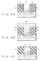
- impurity regions 12 and 13 are formed in a surface portion of a semiconductor silicon substrate 11, and an insulating layer 14 is formed on the substrate 11, as in Embodiment 1.
- Contact holes are formed in an insulating layer 14 to expose the impurity area 12 and impurity area 13, as in Embodiment 1.
- a transition metal layer such as titanium layer 41, is vapor deposited on a resultant semiconductor structure.
- the titanium layer preferably has a thickness of 500 to 1500 ⁇ .
- a transition metal such as titanium
- a vapor deposition method there is a tendency that more particles are oriented in a direction perpendicular to the surface of the substrate, and less transition metal is deposited on the side wall of the contact hole, than by a sputtering method. This tendency is more pronounced with the use of a single vapor deposition source than with the use of plural vapor deposition sources.
- the vapor deposition method therefore, as shown in Fig. 3A, the titanium layer 41 is formed only on the surface of the insulating layer 14 and of the bottom of the contact hole 16 in which case the titanium layer on the bottom of the contact hole is thicker than that on the surface of the insulating layer 14.
- the formation of the transition metal layer by the vapor deposition method can be favorably applied particularly to the contact hole whose aspect ratio is greater.
- Fig. 3A is heat treated to produce a silicide layer 42 and a tungsten layer 43 is grown on the semiconductor structure, as in Embodiment 1 (Fig. 3B).
- the tungsten layer 43 is formed on the surface of the titanium layer 41 and in the contact hole 16.
- the remaining titanium layer 41 and unnecessary tungsten layer portion are eliminated by the etch-back step to leave a tungsten layer portion 43 only in the contact hole 16.
- the remaining titanium layer 41 on the insulating layer 14 can be oxidized to provide a titanium oxide layer.
- tungsten is grown by the CVD method in the same way as set out above, it is not so done on the titanium oxide layer, so that the tungsten layer is provided only in the contact hole 16.
- By removing the titanium oxide layer it is possible to obtain the same structure as shown in Fig. 3C.
- an interconnection layer is connected to the corresponding contact region, as in Embodiment 1, thus producing a semiconductor device.
- Embodiment ensures the same advantages as those in Example 1. Those contact regions which are formed in accordance with Embodiment 3 revealed the same electrical property as that in Example 1.
Landscapes
- Internal Circuitry In Semiconductor Integrated Circuit Devices (AREA)
- Electrodes Of Semiconductors (AREA)
- Chemical Vapour Deposition (AREA)
Claims (3)
- Ein Verfahren zum Bilden eines Kontaktbereichs in einer Halbleitervorrichtung, das die Schritte umfaßt:- Bilden einer Isolierschicht (14) auf einem Halbleitersubstrat (11) mit einem in dem Oberflächenanteil davon gebildeten vorbestimmten Halbleiterbereich, wobei das Halbleitersubstrat (11) Silizium umfaßt;- Versehen eines Kontaktlochs (15, 16) in der Isolierschicht (14), teilweise den Halbleiterbereich freilegend;- Bilden einer Übergangsmetallschicht (17, 31, 41) auf dem freiliegenden Halbleiterbereich;- Bilden einer Silizidschicht (19, 20, 42) durch eine Reaktion der Übergangsmetallschicht (17, 31, 41) mit dem Silizium in dem Substrat (11) innerhalb des Kontaktlochs (15, 16); und- Bilden einer Tungstenschicht (21, 22, 42) mit ausreichender Tiefe durch Gasphasenabscheidung auf der Silizidschicht (19, 20, 42) auf dem Boden des Kontaktlochs, um das Tiefe zu Weite-Verhältnis des Lochs wesentlich zu vermindern.
- Das Verfahren gemäß Anspruch 1,
dadurch gekennzeichnet, daß die Übergangsmetallschicht (17, 31, 41) durch ein Sputtern gebildet wird. - Das Verfahren gemäß Anspruch 2,
dadurch gekennzeichnet, daß das Sputtern ein Magnetronsputtern ist.
Applications Claiming Priority (2)
| Application Number | Priority Date | Filing Date | Title |
|---|---|---|---|
| JP293290/89 | 1989-11-10 | ||
| JP1293290A JP2660072B2 (ja) | 1989-11-10 | 1989-11-10 | コンタクトの形成方法 |
Publications (3)
| Publication Number | Publication Date |
|---|---|
| EP0427254A2 EP0427254A2 (de) | 1991-05-15 |
| EP0427254A3 EP0427254A3 (en) | 1992-06-03 |
| EP0427254B1 true EP0427254B1 (de) | 1997-01-29 |
Family
ID=17792922
Family Applications (1)
| Application Number | Title | Priority Date | Filing Date |
|---|---|---|---|
| EP90121381A Expired - Lifetime EP0427254B1 (de) | 1989-11-10 | 1990-11-08 | Verfahren zum Herstellen einer Kontaktzone |
Country Status (4)
| Country | Link |
|---|---|
| EP (1) | EP0427254B1 (de) |
| JP (1) | JP2660072B2 (de) |
| KR (1) | KR910010667A (de) |
| DE (1) | DE69029836T2 (de) |
Families Citing this family (2)
| Publication number | Priority date | Publication date | Assignee | Title |
|---|---|---|---|---|
| JP3219909B2 (ja) * | 1993-07-09 | 2001-10-15 | 株式会社東芝 | 半導体装置の製造方法 |
| EP0651436A1 (de) * | 1993-10-22 | 1995-05-03 | AT&T Corp. | Verfahren zur Herstellung von Leitern aus Wolfram für integrierte Halbleiter-Schaltkreise |
Family Cites Families (3)
| Publication number | Priority date | Publication date | Assignee | Title |
|---|---|---|---|---|
| JPS62145774A (ja) * | 1985-12-20 | 1987-06-29 | Agency Of Ind Science & Technol | 半導体装置 |
| US4690730A (en) * | 1986-03-07 | 1987-09-01 | Texas Instruments Incorporated | Oxide-capped titanium silicide formation |
| JPS6328867A (ja) * | 1986-07-22 | 1988-02-06 | Ulvac Corp | Cvd法 |
-
1989
- 1989-11-10 JP JP1293290A patent/JP2660072B2/ja not_active Expired - Lifetime
-
1990
- 1990-11-08 EP EP90121381A patent/EP0427254B1/de not_active Expired - Lifetime
- 1990-11-08 DE DE69029836T patent/DE69029836T2/de not_active Expired - Fee Related
- 1990-11-10 KR KR1019900018176A patent/KR910010667A/ko not_active Abandoned
Non-Patent Citations (3)
| Title |
|---|
| 62, 25-26/6/1985 W. METZ & E. BEAM "LPCVD TUNGSTEN METALLISATION FOR MULTILEVEL INTERCONNECT PROCESSES" * |
| IEDM Technical Digest, CH-1973-7, 1983, pages 550-553 by T. Moriya et al. * |
| J.Vacuum Sci. and Tech. vol. 17, No. 4, 1980, by S.P. Murarka. * |
Also Published As
| Publication number | Publication date |
|---|---|
| DE69029836T2 (de) | 1997-06-12 |
| EP0427254A3 (en) | 1992-06-03 |
| EP0427254A2 (de) | 1991-05-15 |
| JPH03153025A (ja) | 1991-07-01 |
| KR910010667A (ko) | 1991-06-29 |
| DE69029836D1 (de) | 1997-03-13 |
| JP2660072B2 (ja) | 1997-10-08 |
Similar Documents
| Publication | Publication Date | Title |
|---|---|---|
| US7443032B2 (en) | Memory device with chemical vapor deposition of titanium for titanium silicide contacts | |
| EP0279588B1 (de) | Kontakt in einer Bohrung in einem Halbleiter und Verfahren zu seiner Herstellung | |
| US5240739A (en) | Chemical vapor deposition technique for depositing titanium silicide on semiconductor wafers | |
| US5278100A (en) | Chemical vapor deposition technique for depositing titanium silicide on semiconductor wafers | |
| US5356835A (en) | Method for forming low resistance and low defect density tungsten contacts to silicon semiconductor wafer | |
| EP0377137B1 (de) | Verfahren zur Selektivabscheidung von refraktorischen Metallen auf Siliziumkörpern | |
| US6309967B1 (en) | Method of forming a contact | |
| US20010006240A1 (en) | Method of forming titanium silicide and titanium by chemical vapor deposition and resulting apparatus | |
| EP0794568A2 (de) | CVD nicht selektive/selektive Aluminiumabscheidung und Reflektivitätsverbesserung unter Verwendung von einer selbstjustierenden ultradünnen Schicht | |
| EP0509835A2 (de) | Herstellungsverfahren für Kontaktteile einer Halbleitervorrichtung | |
| US6888252B2 (en) | Method of forming a conductive contact | |
| EP1412976B1 (de) | Bordotierte titannitridschicht für halbleiter mit grossem aspektverhältnis | |
| US6433434B1 (en) | Apparatus having a titanium alloy layer | |
| EP0427254B1 (de) | Verfahren zum Herstellen einer Kontaktzone | |
| US6597042B1 (en) | Contact with germanium layer | |
| US5837604A (en) | Method for forming interconnection of semiconductor device | |
| JPH05347269A (ja) | 半導体装置の製造方法 | |
| JP2542617B2 (ja) | 半導体装置の製造方法 | |
| US5693561A (en) | Method of integrated circuit fabrication including a step of depositing tungsten | |
| JP2694950B2 (ja) | 高融点金属膜の形成方法 | |
| JP3082934B2 (ja) | 単結晶アルミニウムを用いた半導体装置及びその製造方法 | |
| KR20000007410A (ko) | 반도체 소자의 금속배선 형성방법 | |
| JPH0536625A (ja) | 半導体装置の製造方法 | |
| JPH05175346A (ja) | 配線およびその形成方法 | |
| JPH09139425A (ja) | アルミニウム配線の形成方法 |
Legal Events
| Date | Code | Title | Description |
|---|---|---|---|
| PUAI | Public reference made under article 153(3) epc to a published international application that has entered the european phase |
Free format text: ORIGINAL CODE: 0009012 |
|
| 17P | Request for examination filed |
Effective date: 19901108 |
|
| AK | Designated contracting states |
Kind code of ref document: A2 Designated state(s): DE FR GB |
|
| PUAL | Search report despatched |
Free format text: ORIGINAL CODE: 0009013 |
|
| AK | Designated contracting states |
Kind code of ref document: A3 Designated state(s): DE FR GB |
|
| 17Q | First examination report despatched |
Effective date: 19940420 |
|
| GRAG | Despatch of communication of intention to grant |
Free format text: ORIGINAL CODE: EPIDOS AGRA |
|
| GRAH | Despatch of communication of intention to grant a patent |
Free format text: ORIGINAL CODE: EPIDOS IGRA |
|
| GRAH | Despatch of communication of intention to grant a patent |
Free format text: ORIGINAL CODE: EPIDOS IGRA |
|
| GRAA | (expected) grant |
Free format text: ORIGINAL CODE: 0009210 |
|
| AK | Designated contracting states |
Kind code of ref document: B1 Designated state(s): DE FR GB |
|
| REF | Corresponds to: |
Ref document number: 69029836 Country of ref document: DE Date of ref document: 19970313 |
|
| ET | Fr: translation filed | ||
| PGFP | Annual fee paid to national office [announced via postgrant information from national office to epo] |
Ref country code: GB Payment date: 19971030 Year of fee payment: 8 |
|
| PGFP | Annual fee paid to national office [announced via postgrant information from national office to epo] |
Ref country code: FR Payment date: 19971112 Year of fee payment: 8 |
|
| PLBE | No opposition filed within time limit |
Free format text: ORIGINAL CODE: 0009261 |
|
| STAA | Information on the status of an ep patent application or granted ep patent |
Free format text: STATUS: NO OPPOSITION FILED WITHIN TIME LIMIT |
|
| 26N | No opposition filed | ||
| PG25 | Lapsed in a contracting state [announced via postgrant information from national office to epo] |
Ref country code: GB Free format text: LAPSE BECAUSE OF NON-PAYMENT OF DUE FEES Effective date: 19981108 |
|
| GBPC | Gb: european patent ceased through non-payment of renewal fee |
Effective date: 19981108 |
|
| PG25 | Lapsed in a contracting state [announced via postgrant information from national office to epo] |
Ref country code: FR Free format text: LAPSE BECAUSE OF NON-PAYMENT OF DUE FEES Effective date: 19990730 |
|
| REG | Reference to a national code |
Ref country code: FR Ref legal event code: ST |
|
| PGFP | Annual fee paid to national office [announced via postgrant information from national office to epo] |
Ref country code: DE Payment date: 20071101 Year of fee payment: 18 |
|
| PG25 | Lapsed in a contracting state [announced via postgrant information from national office to epo] |
Ref country code: DE Free format text: LAPSE BECAUSE OF NON-PAYMENT OF DUE FEES Effective date: 20090603 |