EP0427471A2 - Elektrofotokopiermaschine - Google Patents
Elektrofotokopiermaschine Download PDFInfo
- Publication number
- EP0427471A2 EP0427471A2 EP90312020A EP90312020A EP0427471A2 EP 0427471 A2 EP0427471 A2 EP 0427471A2 EP 90312020 A EP90312020 A EP 90312020A EP 90312020 A EP90312020 A EP 90312020A EP 0427471 A2 EP0427471 A2 EP 0427471A2
- Authority
- EP
- European Patent Office
- Prior art keywords
- exposure unit
- photoconductive
- copying machine
- electrophotographic copying
- unit
- Prior art date
- Legal status (The legal status is an assumption and is not a legal conclusion. Google has not performed a legal analysis and makes no representation as to the accuracy of the status listed.)
- Withdrawn
Links
Images


Classifications
-
- G—PHYSICS
- G03—PHOTOGRAPHY; CINEMATOGRAPHY; ANALOGOUS TECHNIQUES USING WAVES OTHER THAN OPTICAL WAVES; ELECTROGRAPHY; HOLOGRAPHY
- G03G—ELECTROGRAPHY; ELECTROPHOTOGRAPHY; MAGNETOGRAPHY
- G03G15/00—Apparatus for electrographic processes using a charge pattern
- G03G15/04—Apparatus for electrographic processes using a charge pattern for exposing, i.e. imagewise exposure by optically projecting the original image on a photoconductive recording material
-
- G—PHYSICS
- G03—PHOTOGRAPHY; CINEMATOGRAPHY; ANALOGOUS TECHNIQUES USING WAVES OTHER THAN OPTICAL WAVES; ELECTROGRAPHY; HOLOGRAPHY
- G03G—ELECTROGRAPHY; ELECTROPHOTOGRAPHY; MAGNETOGRAPHY
- G03G21/00—Arrangements not provided for by groups G03G13/00 - G03G19/00, e.g. cleaning, elimination of residual charge
- G03G21/16—Mechanical means for facilitating the maintenance of the apparatus, e.g. modular arrangements
- G03G21/18—Mechanical means for facilitating the maintenance of the apparatus, e.g. modular arrangements using a processing cartridge, whereby the process cartridge comprises at least two image processing means in a single unit
- G03G21/1803—Arrangements or disposition of the complete process cartridge or parts thereof
- G03G21/181—Manufacturing or assembling, recycling, reuse, transportation, packaging or storage
-
- B—PERFORMING OPERATIONS; TRANSPORTING
- B41—PRINTING; LINING MACHINES; TYPEWRITERS; STAMPS
- B41J—TYPEWRITERS; SELECTIVE PRINTING MECHANISMS, i.e. MECHANISMS PRINTING OTHERWISE THAN FROM A FORME; CORRECTION OF TYPOGRAPHICAL ERRORS
- B41J2/00—Typewriters or selective printing mechanisms characterised by the printing or marking process for which they are designed
- B41J2/435—Typewriters or selective printing mechanisms characterised by the printing or marking process for which they are designed characterised by selective application of radiation to a printing material or impression-transfer material
- B41J2/47—Typewriters or selective printing mechanisms characterised by the printing or marking process for which they are designed characterised by selective application of radiation to a printing material or impression-transfer material using the combination of scanning and modulation of light
- B41J2/471—Typewriters or selective printing mechanisms characterised by the printing or marking process for which they are designed characterised by selective application of radiation to a printing material or impression-transfer material using the combination of scanning and modulation of light using dot sequential main scanning by means of a light deflector, e.g. a rotating polygonal mirror
-
- G—PHYSICS
- G03—PHOTOGRAPHY; CINEMATOGRAPHY; ANALOGOUS TECHNIQUES USING WAVES OTHER THAN OPTICAL WAVES; ELECTROGRAPHY; HOLOGRAPHY
- G03G—ELECTROGRAPHY; ELECTROPHOTOGRAPHY; MAGNETOGRAPHY
- G03G15/00—Apparatus for electrographic processes using a charge pattern
- G03G15/04—Apparatus for electrographic processes using a charge pattern for exposing, i.e. imagewise exposure by optically projecting the original image on a photoconductive recording material
- G03G15/04036—Details of illuminating systems, e.g. lamps, reflectors
- G03G15/04045—Details of illuminating systems, e.g. lamps, reflectors for exposing image information provided otherwise than by directly projecting the original image onto the photoconductive recording material, e.g. digital copiers
-
- G—PHYSICS
- G03—PHOTOGRAPHY; CINEMATOGRAPHY; ANALOGOUS TECHNIQUES USING WAVES OTHER THAN OPTICAL WAVES; ELECTROGRAPHY; HOLOGRAPHY
- G03G—ELECTROGRAPHY; ELECTROPHOTOGRAPHY; MAGNETOGRAPHY
- G03G21/00—Arrangements not provided for by groups G03G13/00 - G03G19/00, e.g. cleaning, elimination of residual charge
- G03G21/16—Mechanical means for facilitating the maintenance of the apparatus, e.g. modular arrangements
- G03G21/18—Mechanical means for facilitating the maintenance of the apparatus, e.g. modular arrangements using a processing cartridge, whereby the process cartridge comprises at least two image processing means in a single unit
- G03G21/1803—Arrangements or disposition of the complete process cartridge or parts thereof
- G03G21/1814—Details of parts of process cartridge, e.g. for charging, transfer, cleaning, developing
-
- G—PHYSICS
- G03—PHOTOGRAPHY; CINEMATOGRAPHY; ANALOGOUS TECHNIQUES USING WAVES OTHER THAN OPTICAL WAVES; ELECTROGRAPHY; HOLOGRAPHY
- G03G—ELECTROGRAPHY; ELECTROPHOTOGRAPHY; MAGNETOGRAPHY
- G03G15/00—Apparatus for electrographic processes using a charge pattern
- G03G15/04—Apparatus for electrographic processes using a charge pattern for exposing, i.e. imagewise exposure by optically projecting the original image on a photoconductive recording material
- G03G15/043—Apparatus for electrographic processes using a charge pattern for exposing, i.e. imagewise exposure by optically projecting the original image on a photoconductive recording material with means for controlling illumination or exposure
- G03G15/0435—Apparatus for electrographic processes using a charge pattern for exposing, i.e. imagewise exposure by optically projecting the original image on a photoconductive recording material with means for controlling illumination or exposure by introducing an optical element in the optical path, e.g. a filter
-
- G—PHYSICS
- G03—PHOTOGRAPHY; CINEMATOGRAPHY; ANALOGOUS TECHNIQUES USING WAVES OTHER THAN OPTICAL WAVES; ELECTROGRAPHY; HOLOGRAPHY
- G03G—ELECTROGRAPHY; ELECTROPHOTOGRAPHY; MAGNETOGRAPHY
- G03G2221/00—Processes not provided for by group G03G2215/00, e.g. cleaning or residual charge elimination
- G03G2221/16—Mechanical means for facilitating the maintenance of the apparatus, e.g. modular arrangements and complete machine concepts
- G03G2221/1636—Mechanical means for facilitating the maintenance of the apparatus, e.g. modular arrangements and complete machine concepts for the exposure unit
-
- G—PHYSICS
- G03—PHOTOGRAPHY; CINEMATOGRAPHY; ANALOGOUS TECHNIQUES USING WAVES OTHER THAN OPTICAL WAVES; ELECTROGRAPHY; HOLOGRAPHY
- G03G—ELECTROGRAPHY; ELECTROPHOTOGRAPHY; MAGNETOGRAPHY
- G03G2221/00—Processes not provided for by group G03G2215/00, e.g. cleaning or residual charge elimination
- G03G2221/16—Mechanical means for facilitating the maintenance of the apparatus, e.g. modular arrangements and complete machine concepts
- G03G2221/1651—Mechanical means for facilitating the maintenance of the apparatus, e.g. modular arrangements and complete machine concepts for connecting the different parts
- G03G2221/1654—Locks and means for positioning or alignment
-
- G—PHYSICS
- G03—PHOTOGRAPHY; CINEMATOGRAPHY; ANALOGOUS TECHNIQUES USING WAVES OTHER THAN OPTICAL WAVES; ELECTROGRAPHY; HOLOGRAPHY
- G03G—ELECTROGRAPHY; ELECTROPHOTOGRAPHY; MAGNETOGRAPHY
- G03G2221/00—Processes not provided for by group G03G2215/00, e.g. cleaning or residual charge elimination
- G03G2221/16—Mechanical means for facilitating the maintenance of the apparatus, e.g. modular arrangements and complete machine concepts
- G03G2221/18—Cartridge systems
- G03G2221/183—Process cartridge
Definitions
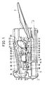
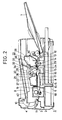
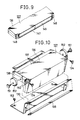
- the linear light emitting head 46 is formed by linearly arranging a plurality of end emission electroluminescent elements.
- Each end emission electroluminescent element is formed by sandwiching an active thin film, such as a thin film of zinc sulfide containing an active element, between dielectric thin films and attaching electrodes respectively to the dielectric thin films. Voltage is applied individually across the pairs of electrodes to make the end emission electroluminescent elements emit light individually.
- Slots 55 for receiving the screws 45 therethrough are formed in the inclined wall 43 of the frame 42 so that the plate 44 can be moved along the inclined wall 44 and fastened to the same at an optional position in adjusting the gap between the linear light emitting head 46 and the circumference of the photoconductive drum 24.
- the respective image forming points of the exposure units 31 and 32 as disposed in the housing chamber 33 on the circumference of the photoconductive drum 24 coincide with each other.
- the optical path is fixed with respect to the photoconductive drum 24 when the electrophotographic copying machine is equipped with either the exposure unit 31 or the exposure unit 32, the parts of the units other than those of the exposure unit 31 or 32 can he arranged closely, so that the electrophotographic copying machine can be formed in a compact construction.
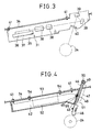
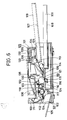
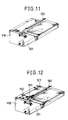
- the edge of the rear wall 147a of the light emitting section with respect to the rotating direction of the photoconductive drum 121 is closer to the circumference of the photoconductive drum 121 than the edge of the front wall of the light emitting section.
- reference faces 148 are formed opposite to the circumference of the photoconductive drum 121 respectively in the opposite ends of the light emitting section of the case 136.
- lugs each provided with a vertical slot 150 project respectively from the upper opposite ends of the light emitting section of the case 136.
- Screws 134 are screwed through the slots 150 in the holding plate 130 to fasten the case 136 to the holding plate 130.
- Eccentric cams 152 are fixed to the opposite sides of the case 136 with screws 151, respectively.
- the holding plate 130 is fixed to the holding frame 118 with screws 153.
Landscapes
- Physics & Mathematics (AREA)
- General Physics & Mathematics (AREA)
- Engineering & Computer Science (AREA)
- Computer Vision & Pattern Recognition (AREA)
- Life Sciences & Earth Sciences (AREA)
- Manufacturing & Machinery (AREA)
- Sustainable Development (AREA)
- Electrophotography Configuration And Component (AREA)
- Exposure Or Original Feeding In Electrophotography (AREA)
Applications Claiming Priority (4)
| Application Number | Priority Date | Filing Date | Title |
|---|---|---|---|
| JP291663/89 | 1989-11-09 | ||
| JP1291663A JPH03152577A (ja) | 1989-11-09 | 1989-11-09 | 電子写真装置 |
| JP1316942A JPH03177856A (ja) | 1989-12-06 | 1989-12-06 | 電子写真装置 |
| JP316942/89 | 1989-12-06 |
Publications (2)
| Publication Number | Publication Date |
|---|---|
| EP0427471A2 true EP0427471A2 (de) | 1991-05-15 |
| EP0427471A3 EP0427471A3 (en) | 1992-07-01 |
Family
ID=26558642
Family Applications (1)
| Application Number | Title | Priority Date | Filing Date |
|---|---|---|---|
| EP19900312020 Withdrawn EP0427471A3 (en) | 1989-11-09 | 1990-11-02 | Electrophotographic copying machine |
Country Status (2)
| Country | Link |
|---|---|
| EP (1) | EP0427471A3 (de) |
| KR (1) | KR910010254A (de) |
Cited By (2)
| Publication number | Priority date | Publication date | Assignee | Title |
|---|---|---|---|---|
| EP0621515A3 (de) * | 1993-04-21 | 1998-03-11 | Kabushiki Kaisha TEC | Bilderzeugungsgerät mit einem lichtempfindlichen Teil |
| WO2000011624A1 (en) | 1998-08-25 | 2000-03-02 | Telefonaktiebolaget Lm Ericsson (Publ) | Smart card wallet |
Family Cites Families (4)
| Publication number | Priority date | Publication date | Assignee | Title |
|---|---|---|---|---|
| JPH0697326B2 (ja) * | 1984-02-07 | 1994-11-30 | 三田工業株式会社 | ユニット型複写機 |
| US4752806A (en) * | 1986-06-23 | 1988-06-21 | Xerox Corporation | Multi-mode imaging system |
| US4785319A (en) * | 1986-08-05 | 1988-11-15 | Canon Kabushiki Kaisha | Electrographic apparatus |
| JPH0682245B2 (ja) * | 1987-12-22 | 1994-10-19 | キヤノン株式会社 | 画像形成装置 |
-
1990
- 1990-10-13 KR KR1019900016243A patent/KR910010254A/ko not_active Abandoned
- 1990-11-02 EP EP19900312020 patent/EP0427471A3/en not_active Withdrawn
Cited By (2)
| Publication number | Priority date | Publication date | Assignee | Title |
|---|---|---|---|---|
| EP0621515A3 (de) * | 1993-04-21 | 1998-03-11 | Kabushiki Kaisha TEC | Bilderzeugungsgerät mit einem lichtempfindlichen Teil |
| WO2000011624A1 (en) | 1998-08-25 | 2000-03-02 | Telefonaktiebolaget Lm Ericsson (Publ) | Smart card wallet |
Also Published As
| Publication number | Publication date |
|---|---|
| KR910010254A (ko) | 1991-06-29 |
| EP0427471A3 (en) | 1992-07-01 |
Similar Documents
| Publication | Publication Date | Title |
|---|---|---|
| US7619643B2 (en) | Method and apparatus for image forming capable of effectively avoiding an adverse temperature effect to an optical scanning system | |
| US8004552B2 (en) | Optical scanning device and image forming apparatus | |
| US5095337A (en) | Electrophotographic apparatus having a movable self-scanner | |
| US7151557B2 (en) | Collimation assembly for adjusting laser light sources in a multi-beamed laser scanning unit | |
| EP2584776B1 (de) | Bildlesevorrichtung und Bilderzeugungsvorrichtung | |
| US5113291A (en) | Optical axis and focus adjustment mechanism for semiconductor laser and collimator lens | |
| US5299051A (en) | Housing structure for optical scanning system | |
| US6750997B2 (en) | Scanning device and image forming apparatus | |
| EP0427471A2 (de) | Elektrofotokopiermaschine | |
| US5774324A (en) | Scorotron charger for use in an image forming apparatus | |
| JP2885288B2 (ja) | 光走査装置 | |
| US5001499A (en) | Light scanning apparatus and image forming apparatus utilizing same | |
| JP3347479B2 (ja) | 走査光学装置の取付け構造 | |
| JPH10138559A (ja) | 画像形成装置 | |
| JP2938175B2 (ja) | 光書込み装置 | |
| JP2857640B2 (ja) | 画像記録装置 | |
| JP3471902B2 (ja) | 光源装置 | |
| JP3533070B2 (ja) | レーザーユニット、光書込装置、画像形成装置 | |
| JPH0820130A (ja) | 光学装置 | |
| JP4203213B2 (ja) | 半導体レーザアレイパッケージ・半導体レーザアレイ光源ユニット・マルチビーム走査装置および画像形成装置 | |
| JPS58205171A (ja) | 静電プリンタ | |
| JP2007183326A (ja) | 走査光学装置及び画像形成装置 | |
| JPS63221367A (ja) | 画像記録装置 | |
| JPH0821971A (ja) | 走査光学装置 | |
| JPH0822174A (ja) | 画像形成装置における走査光学装置 |
Legal Events
| Date | Code | Title | Description |
|---|---|---|---|
| PUAI | Public reference made under article 153(3) epc to a published international application that has entered the european phase |
Free format text: ORIGINAL CODE: 0009012 |
|
| 17P | Request for examination filed |
Effective date: 19901113 |
|
| AK | Designated contracting states |
Kind code of ref document: A2 Designated state(s): DE FR GB IT NL |
|
| PUAL | Search report despatched |
Free format text: ORIGINAL CODE: 0009013 |
|
| AK | Designated contracting states |
Kind code of ref document: A3 Designated state(s): DE FR GB IT NL |
|
| 17Q | First examination report despatched |
Effective date: 19930528 |
|
| STAA | Information on the status of an ep patent application or granted ep patent |
Free format text: STATUS: THE APPLICATION HAS BEEN WITHDRAWN |
|
| 18W | Application withdrawn |
Withdrawal date: 19930827 |