EP0428049B1 - Méthode de connexion entre guide d'onde et fibre optique - Google Patents
Méthode de connexion entre guide d'onde et fibre optique Download PDFInfo
- Publication number
- EP0428049B1 EP0428049B1 EP90121296A EP90121296A EP0428049B1 EP 0428049 B1 EP0428049 B1 EP 0428049B1 EP 90121296 A EP90121296 A EP 90121296A EP 90121296 A EP90121296 A EP 90121296A EP 0428049 B1 EP0428049 B1 EP 0428049B1
- Authority
- EP
- European Patent Office
- Prior art keywords
- layers
- waveguide substrate
- layer
- optical fiber
- waveguide
- Prior art date
- Legal status (The legal status is an assumption and is not a legal conclusion. Google has not performed a legal analysis and makes no representation as to the accuracy of the status listed.)
- Expired - Lifetime
Links
Images



Classifications
-
- G—PHYSICS
- G02—OPTICS
- G02B—OPTICAL ELEMENTS, SYSTEMS OR APPARATUS
- G02B6/00—Light guides; Structural details of arrangements comprising light guides and other optical elements, e.g. couplings
- G02B6/24—Coupling light guides
- G02B6/42—Coupling light guides with opto-electronic elements
- G02B6/4201—Packages, e.g. shape, construction, internal or external details
- G02B6/4204—Packages, e.g. shape, construction, internal or external details the coupling comprising intermediate optical elements, e.g. lenses, holograms
- G02B6/4212—Packages, e.g. shape, construction, internal or external details the coupling comprising intermediate optical elements, e.g. lenses, holograms the intermediate optical element being a coupling medium interposed therebetween, e.g. epoxy resin, refractive index matching material, index grease, matching liquid or gel
-
- G—PHYSICS
- G02—OPTICS
- G02B—OPTICAL ELEMENTS, SYSTEMS OR APPARATUS
- G02B6/00—Light guides; Structural details of arrangements comprising light guides and other optical elements, e.g. couplings
- G02B6/24—Coupling light guides
- G02B6/26—Optical coupling means
- G02B6/30—Optical coupling means for use between fibre and thin-film device
-
- Y—GENERAL TAGGING OF NEW TECHNOLOGICAL DEVELOPMENTS; GENERAL TAGGING OF CROSS-SECTIONAL TECHNOLOGIES SPANNING OVER SEVERAL SECTIONS OF THE IPC; TECHNICAL SUBJECTS COVERED BY FORMER USPC CROSS-REFERENCE ART COLLECTIONS [XRACs] AND DIGESTS
- Y10—TECHNICAL SUBJECTS COVERED BY FORMER USPC
- Y10S—TECHNICAL SUBJECTS COVERED BY FORMER USPC CROSS-REFERENCE ART COLLECTIONS [XRACs] AND DIGESTS
- Y10S359/00—Optical: systems and elements
- Y10S359/90—Methods
Definitions
- This invention relates to a connecting method between a waveguide substrate made of electro-optical crystal and an optical fiber.
- the invention is directed to a method of connecting a waveguide substrate made of electro-optical crystal and an optical fiber by means of a bonding agent of the ultraviolet light curing type, comprising the steps of: forming, at least at and around a portion of an end face of the waveguide substrate at which an end face of the optical fiber is to be closely contacted, a reflection preventing film arranged to pass therethrough light of a wavelength which is to be transmitted by way of the optical fiber and to prevent reflection of said wavelength at said end face, contacting the end face of the optical fiber closely with the reflection preventing film with the bonding agent of the ultraviolet light curing type applied to the end face of the optical fiber, bringing the waveguide substrate and the optical fiber into optical alignment, and irradiating the bonding agent with ultraviolet rays upon the end face of the waveguide substrate from the side on which the reflection preventing film is formed to cure it.
- optical apparatus such as an optical modulator and an optical switch are required in addition to basic components such as a light source apparatus and a light receiving apparatus.
- One of forms of optical apparatus is a waveguide type.
- An optical apparatus of the waveguide type is normally constituted such that a waveguide is formed on a waveguide substrate made of electro-optical crystal and a phase and so forth of a beam of light confined in the waveguide are controlled.
- An optical apparatus of the waveguide type has an advantage that, due to its structure, miniaturization can be achieved readily and it can be mass-produced using the planer process or the like as well as another advantage that an electric field can be applied effectively and the power consumption can be reduced significantly.
- the optical fiber as an optical transmission line and a waveguide substrate must necessarily be connected to each other both optically and mechanically. Thus, optimization of a connecting method is being sought.
- reference numeral 2 denotes a waveguide substrate, 4 a waveguide formed on the waveguide substrate 2, and 6 an optical fiber to be connected.
- a bonding agent 8 of the ultraviolet light curing type is applied to an end portion of the optical fiber 6 as shown in FIG.
- Electro-optical crystal which makes a material of a waveguide substrate is particularly LiNbO3 or LiTaO3.
- the conventional method is applied to a waveguide substrate made of one of such materials, there is a problem that the waveguide may suffer from optical damage due to an influence of ultraviolet rays which are irradiated in order to cause a bonding agent to cure.
- optical damage signifies a phenomenon that, when light such as ultraviolet light of a comparatively high intensity is irradiated upon electro-optical crystal of LiNbO3 or the like, excited electrons drop in, in a process in which electrons are excited from an impurity level in the crystal to a conduction band, to a trap level, and a local electric field is produced in the inside of the crystal so that the refraction index is locally varied by way of an electro-optical effect.
- Such optical damage is recognized as a reversible phenomenon, and after the irradiation of ultraviolet light is stopped, the variation in refractive index is cancelled. However, since such cancellation does not necessarily proceed quickly, optical damage actually matters when an optical apparatus is used.
- the refractive index of a waveguide is locally varied by optical damage in this manner, the loss characteristics of the optical apparatus of the waveguide type may be deteriorated or the operating point (for example, a bias potential in the case of an optical modulator of the waveguide type) may be varied.
- a method of connecting a waveguide substrate made of electro-optical crystal and an optical fiber by means of a bonding agent of the ultraviolet light curing type comprising the steps of: forming, at least at and around a portion of an end face of the waveguide substrate at which an end face of the optical fiber is to be closely contacted, a reflection preventing film arranged to pass therethrough light of a wavelength which is to be transmitted by way of the optical fiber and to prevent reflection of said wavelength at said end face, contacting the end face of the optical fiber closely with the reflection preventing film with the bonding agent of the ultraviolet light curing type applied to the end face of the optical fiber, bringing the waveguide substrate and the optical fiber into optical alignment, and irradiating the bonding agent with ultraviolet rays upon the end face of the waveguide substrate from the side on which the reflection preventing film is formed to cure it, and wherein the reflection preventing film is arranged to block ultraviolet light of the wavelength with which the bonding agent cures.
- the connecting method further comprises the step of transmitting ultraviolet rays in the optical fiber to cause the bonding agent to cure.
- an optical assembly comprising an optical fiber optically coupled to a waveguide on a waveguide substrate, wherein said waveguide substrate is made of electro-optical crystal and has at least one waveguide formed thereon, a reflection preventing film is formed on an end face of said waveguide substrate and is arranged to have an ultraviolet light blocking function while passing therethrough light of a wavelength which is to be transmitted by way of the optical fiber and preventing reflection of said wavelength at said end face, and wherein an optical fiber is adhered to said reflection preventing film in optical alignment with said waveguide of said waveguide substrate by means of a cured bonding agent of the ultraviolet light curing type.
- the reflection preventing film may comprise Si layers and SiO2 layers laminated alternately to form a plurality of layers on the waveguide substrate made of electro-optical crystal.
- the number of Si and SiO2 layers may range from 5 to 10. Selection of materials of individual layers and design values of thicknesses of individual layers are defined specifically in accordance with the number of layers.
- the reflection preventing film with an ultraviolet light intercepting function which is used in the method of the present invention can be reduced in Fresnel loss to reduce connection loss because it has a reflection preventing function for light of a wavelength to be transmitted.
- the reflection preventing film can pass therethrough light of a band of the wavelength of 1.55 ⁇ m to be transmitted by way of the optical fiber but can intercept, at a high intercepting rate, ultraviolet rays with which the bonding agent cures.
- FIG. 2 is a perspective view of an optical apparatus of the waveguide type which is used in an embodiment of the present invention, and the optical apparatus particularly is an optical modulator which intensity modulates a laser beam received with a fixed intensity and outputs the modulated light.
- the apparatus is constituted such that a waveguide 4 of the Mach-Zehnder type is formed by partly diffusing, for example, Ti (titanium) into a waveguide substrate 2 made of LiNbO3 , and a pair of electrodes 12 and 14 for the application of a driving voltage are mounted at branching portions 4a and 4b of the waveguide 4.
- each of the branching portions 4a and 4b of the waveguide varies in response to an electric field applied thereto, if a potential difference is applied between the electrodes 12 and 14, then beams of light branched in same phases will undergo different phase variations.
- the waveguide 4 is a single mode waveguide which transmits only light of a basic mode except the Y-branching portion, when the phase difference between the branched beams of light when they are to be combined is equal to 0, the intensity of interference light to be outputted is maximum, but when the phase difference of the branched beams of light when they are to be combined is equal to ⁇ , the intensity of interference light is minimum.
- phase difference assumes a value between 0 and ⁇
- interference light has an intensity depending upon the phase difference.
- a light intensity modulating function is achieved by changing the voltage to be applied between the electrodes 12 and 14 in response to a modulating signal.
- the operation characteristics may be varied over a wide range by an influence of such optical damage as described above.
- a method of the present invention is applied to such connection between an optical apparatus and an optical fiber.
- a reflection preventing film 10 with an ultraviolet light intercepting function of passing therethrough light of a band of a wavelength of 1.55 ⁇ m but intercepting ultraviolet rays of a wavelength of 0.43 ⁇ m is formed at least at and around a portion of an end face of a waveguide substrate 2 at which an end face of an optical fiber 6 is to be closely contacted as shown in FIG. 3A.
- the wavelength of light to pass through the reflection preventing film 10 may be, in addition to the 1.55 ⁇ m band as described above, a 1.3 ⁇ m band.
- the wavelength of ultraviolet rays is not limited to 0.43 ⁇ m, but ultraviolet rays of any other wavelength with which a bonding agent of the ultraviolet light curing type cures may be used.
- the reflection preventing film 10 can be formed by an ordinary method such as electron beam vapor deposition. In the present embodiment, the reflection preventing film 10 is formed on, an entire end face of the waveguide substrate 2.
- a bonding agent 8 of the ultraviolet light curing type is applied to an end portion of the optical fiber 6 to be connected as shown in FIG. 3A.
- the bonding agent 8 may be applied to and around a corresponding portion of the reflection preventing film 10 on the waveguide 4.
- the end face of the optical fiber 6 is closely contacted with the reflection preventing film 10 such that the end face of the core of the optical fiber 6 may be opposed to the end face of the waveguide 4 with the bonding agent 8 applied to the end face of the optical fiber 6.
- adjustment of the relative positional relationship between the optical fiber 6 and the waveguide substrate 2 can be performed while measuring an actual optical coupling efficiency between them.
- ultraviolet rays are irradiated upon the bonding agent 8 applied to the reflection preventing film 10 in a direction substantially perpendicular to the end face of the waveguide substrate 2 as indicated by arrow marks A in FIG. 3B to cause the bonding agent 8 to cure.
- the bonding agent 8 cures from an outer peripheral portion thereof by irradiation of ultraviolet rays
- a central portion of the bonding agent 8 may not cure by irradiation of ultraviolet rays for a comparatively short period of time, and accordingly, it is desirable to transmit ultraviolet rays in the optical fiber 6 to positively cause the central portion of the bonding agent 8 to cure.
- ultraviolet rays are irradiated in a direction substantially perpendicular to the end face of the waveguide substrate 2, such a situation will not take place that ultraviolet rays are admitted directly into the waveguide 4 to cause optical damage to the waveguide 4.
- the direction of irradiation of ultraviolet rays is not limited to such perpendicular direction as shown in FIG. 3B, but ultraviolet rays may be irradiated from an obliquely upper position upon the end face of the waveguide substrate 2 on which the reflection preventing film 10 is formed.
- the reflection preventing film 10 with an ultraviolet right intercepting function is formed on the end face of the waveguide substrate 2, such a situation will not take place that ultraviolet rays irradiated are admitted into the waveguide substrate 2 by way of the end face thereof and then into the waveguide 4. Further, since ultraviolet rays reflected from the reflection preventing film 10 are radiated in a direction in which they go away from the waveguide substrate 2, that is, in the direction indicated by arrow marks B in FIG. 3B, the waveguide 4 will not suffer from optical damage by such reflected light. Accordingly, when connection between an optical fiber and a waveguide substrate is to be performed by the present method, characteristics of an optical apparatus of the waveguide type will not be put into an unstable condition by an influence of optical damage.
- the reflection preventing film is formed by laminating a Si layer and a SiO2 layer alternately by 5 to 10 layers on a waveguide substrate made of electro-optical crystal, and selection of materials of individual layers and design values of the individual layers are such as given in the following tables for the numbers of layers.
- a value indicative of a film thickness is a relative value when the film thickness corresponding to one fourth a central wavelength of ultraviolet light to be intercepted is represented by 1.0.
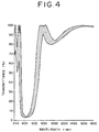
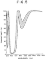
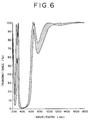
- the characteristic curves can take when the deviation in film thickness among individual layers is ⁇ 10 % where the number of layers of a reflection preventing film with an ultraviolet light intercepting function is 5 to 10 as given above are shown in FIGS. 4 to 9, respectively.
- Those layer structures are optimally designed for the case wherein the angle of incidence is 0 degrees, and as far as the deviation in thickness among layers remains within the above range, the layer structures have a transmission factor of higher than 99.5 % with regard to light of the wavelength of 1.55 ⁇ m. Accordingly, they present a sufficient reflection preventing function with regard to light to be transmitted having wavelength of the 1.55 ⁇ m band.
- the deviation in film thickness among individual layers remains within the range described above, they can present a sufficient intercepting function with regard to ultraviolet rays having a wavelength of 0.43 ⁇ m. While the intercepting function to ultraviolet rays increases as the number of layers increases, the number of layers of Si and SiO2 layers is sufficient with 5 to 10 in practical use.
Landscapes
- Physics & Mathematics (AREA)
- General Physics & Mathematics (AREA)
- Optics & Photonics (AREA)
- Optical Integrated Circuits (AREA)
- Optical Couplings Of Light Guides (AREA)
- Lining Or Joining Of Plastics Or The Like (AREA)
Claims (10)
- Procédé de connexion d'un substrat de guide d'ondes réalisé en un cristal électro-optique et d'une fibre optique au moyen d'un agent de liaison du type durcissement à la lumière ultraviolette, comprenant les étapes de :formation, au moins au niveau et autour d'une partie d'une face d'extrémité du substrat de guide d'ondes (2) au niveau de laquelle une face d'extrémité de la fibre optique (6) est amenée en contact intime, d'un film d'empêchement de réflexion (10) agencé pour laisser passer au travers la lumière d'une longueur d'onde qui doit être transmise au moyen de la fibre optique (6) et pour empêcher la réflexion de ladite longueur d'onde au niveau de ladite face d'extrémité ;mise en contact de la face d'extrémité de la fibre optique (6) de façon intime avec le film d'empêchement de réflexion (10) à l'aide de l'agent de liaison (8) du type durcissement à la lumière ultraviolette appliqué sur la face d'extrémité de la fibre optique (6) ;amenée du substrat de guide d'ondes (2) et de la fibre optique (6) en alignement optique ; etirradiation de l'agent de liaison (8) avec des rayons ultraviolets sur la face d'extrémité du substrat de guide d'ondes (2) depuis le côté sur lequel le film d'empêchement de réflexion (10) est formé afin de le durcir,caractérisé en ce que le film d'empêchement de réflexion (10) est agencé pour bloquer la lumière ultraviolette de la longueur d'onde à l'aide de laquelle l'agent de liaison (8) durcit.
- Procédé selon la revendication 1, comprenant en outre l'étape de transmission de rayons ultraviolets dans la fibre optique afin de forcer l'agent de liaison (8) à durcir.
- Procédé selon la revendication 1, dans lequel des rayons ultraviolets sont irradiés suivant une direction sensiblement perpendiculaire à la face d'extrémité du substrat de guide d'ondes (2).
- Assemblage optique comprenant une fibre optique couplée optiquement à un guide d'ondes sur un substrat de guide d'ondes, dans lequel :ledit substrat de guide d'ondes (2) est réalisé en un cristal électro-optique et il comporte au moins un guide d'ondes (4) formé dessus ;un film d'empêchement de réflexion (10) est formé sur une face d'extrémité dudit substrat de guide d'ondes (2) et est agencé de manière à présenter une fonction de blocage de la lumière ultraviolette tout en laissant passer au travers la lumière d'une longueur d'onde qui doit être transmise au moyen de la fibre optique et tout en empêchant la réflexion de ladite longueur d'onde au niveau de ladite face d'extrémité ; etdans lequel une fibre optique (6) est collée audit film d'empêchement de réflexion (10) en alignement optique avec ledit guide d'ondes dudit substrat de guide d'ondes (2) au moyen d'un agent de liaison durci (8) du type durcissement à la lumière ultraviolette.
- Procédé selon la revendication 1, 2 ou 3 ou assemblage selon la revendication 4, dans lequel le film d'empêchement de réflexion (10) comprend des couches en Si et des couches en SiO₂ stratifiées en alternance afin de former cinq couches sur ledit substrat de guide d'ondes (2) réalisé en un cristal électro-optique, la première couche qui entre en contact direct avec ledit substrat de guide d'ondes (2) étant une couche en Si et l'épaisseur de film égale à un quart de la longueur d'onde centrale de la lumière ultraviolette à intercepter étant représentée en tant que 1,0, les valeurs de conception des épaisseurs de film des première à cinquième couches étant respectivement égales à 1,09, 0,92, 0,96, 1,07 et 0,91.
- Procédé selon la revendication 1, 2 ou 3 ou assemblage selon la revendication 4, dans lequel le film d'empêchement de réflexion (10) comprend une couche en Si et une couche en SiO₂ stratifiées en alternance afin de former six couches sur ledit substrat de guide d'ondes (2) réalisé en un cristal électro-optique, la première couche qui est en contact direct avec ledit substrat de guide d'ondes (2) étant une couche en SiO₂, et où l'épaisseur de film égale à un quart de la longueur d'onde centrale de la lumière ultraviolette à intercepter est représentée en tant que 1,0, les valeurs de conception des épaisseurs de film des première à sixième couches étant respectivement égales à 0,83, 1,25, 0,96, 0,84, 1,24 et 0,82.
- Procédé selon la revendication 1, 2 ou 3 ou assemblage selon la revendication 4, dans lequel le film d'empêchement de réflexion (10) comprend des couches en Si et des couches en SiO₂ stratifiées en alternance afin de former sept couches sur ledit substrat de guide d'ondes (2) réalisé en un cristal électro-optique, la première couche qui est en contact direct avec ledit substrat de guide d'ondes (2) étant une couche en Si, et où l'épaisseur de film égale à un quart de la longueur d'onde centrale de la lumière ultraviolette à intercepter est représentée en tant que 1,0, les valeurs de conception des épaisseurs de film des première à septième couches étant respectivement égales à 0,87, 0,85, 1,24, 0,79, 0,82, 1,29 et 0,70.
- Procédé selon la revendication 1, 2 ou 3 ou assemblage selon la revendication 4, dans lequel le film d'empêchement de réflexion (10) comprend des couches en Si et des couches en SiO₂ stratifiées en alternance afin de former huit couches sur ledit substrat de guide d'ondes (2) réalisé en un cristal électro-optique, la première couche qui est en contact direct avec ledit substrat de guide d'ondes (2) étant une couche en SiO₂, et où l'épaisseur de film égale à un quart de la longueur d'onde centrale de la lumière ultraviolette à intercepter est représentée en tant que 1,0, les valeurs de conception des épaisseurs de film des première à huitième couches étant respectivement égales à 1,11, 0,92, 0,96, 1,10, 0,89, 1,00, 1,09 et 0,87.
- Procédé selon la revendication 1, 2 ou 3 ou assemblage selon la revendication 4, dans lequel ledit film d'empêchement de réflexion (10) comprend des couches en Si et des couches en SiO₂ stratifiées en alternance afin de former neuf couches sur ledit substrat de guide d'ondes (2) réalisé en un cristal électro-optique, la première couche qui est en contact direct avec ledit substrat de guide d'ondes (2) étant une couche en Si, et où l'épaisseur de film égale à un quart de la longueur d'onde centrale de la lumière ultraviolette à intercepter est représentée en tant que 1,0, les valeurs de conception des épaisseurs de film des première à neuvième couches étant respectivement égales à 0,70, 1,27, 0,99, 0,83, 1,21, 0,93, 0,86, 1,26 et 0,80.
- Procédé selon la revendication 1, 2 ou 3 ou assemblage selon la revendication 4, dans lequel ledit film d'empêchement de réflexion (10) comprend des couches en Si et des couches en SiO₂ stratifiées en alternance afin de former dix couches sur ledit substrat de guide d'ondes (2) réalisé en un cristal électro-optique, la première couche étant une couche en SiO₂, et où l'épaisseur de film égale à un quart de la longueur d'onde centrale de la lumière ultraviolette à intercepter est représentée en tant que 1,0, les valeurs de conception des épaisseurs de film des première à dixième couches étant respectivement égales à 0,93, 0,92, 1,35, 1,00, 0,87, 1,23, 1,00, 0,86, 1,17 et 0,50.
Applications Claiming Priority (2)
| Application Number | Priority Date | Filing Date | Title |
|---|---|---|---|
| JP288731/89 | 1989-11-08 | ||
| JP1288731A JPH03150509A (ja) | 1989-11-08 | 1989-11-08 | 導波路基板と光ファイバの接続方法及び該方法の実施に使用する紫外光遮断機能付き反射防止膜 |
Publications (3)
| Publication Number | Publication Date |
|---|---|
| EP0428049A2 EP0428049A2 (fr) | 1991-05-22 |
| EP0428049A3 EP0428049A3 (en) | 1992-07-08 |
| EP0428049B1 true EP0428049B1 (fr) | 1996-04-10 |
Family
ID=17733959
Family Applications (1)
| Application Number | Title | Priority Date | Filing Date |
|---|---|---|---|
| EP90121296A Expired - Lifetime EP0428049B1 (fr) | 1989-11-08 | 1990-11-07 | Méthode de connexion entre guide d'onde et fibre optique |
Country Status (5)
| Country | Link |
|---|---|
| US (1) | US5107535A (fr) |
| EP (1) | EP0428049B1 (fr) |
| JP (1) | JPH03150509A (fr) |
| CA (1) | CA2029411C (fr) |
| DE (1) | DE69026471T2 (fr) |
Families Citing this family (10)
| Publication number | Priority date | Publication date | Assignee | Title |
|---|---|---|---|---|
| FR2674033B1 (fr) * | 1991-03-14 | 1993-07-23 | Corning Inc | Composant optique integre a liaison entre un guide d'onde integre et une fibre optique, fonctionnant dans un large domaine de temperature. |
| US5282071A (en) * | 1992-07-13 | 1994-01-25 | Motorola, Inc. | Contact areas on an optical waveguide and method of making |
| EP0652451B1 (fr) * | 1993-11-08 | 2001-08-08 | Corning Incorporated | Couplage de guides d'onde optique planaire et fibres optiques à rétroreflexion réduite |
| US5337383A (en) * | 1993-11-09 | 1994-08-09 | The United States Of America As Represented By The Secretary Of The Army | Method for internal laser welding of metallized optical components for attachment of optical fibers |
| US5926594A (en) * | 1994-08-31 | 1999-07-20 | Litton Systems, Inc. | System and method for aligning and attaching optical fibers to optical waveguides, and products obtained thereby |
| FR2798741A1 (fr) * | 1999-09-21 | 2001-03-23 | Corning Inc | Procede de raccordement par fusion d'une fibre optique a un dispositif optique integre et structures resultantes |
| FR2809500B1 (fr) * | 2000-05-29 | 2003-09-26 | Highwave Optical Tech | Procede et dispositif de conditionnement de composant a fibres optiques |
| US6599957B2 (en) | 2001-05-07 | 2003-07-29 | Corning Incorporated | Photosensitive material suitable for making waveguides and method of making waveguides utilizing this photosensitive optical material |
| US6744951B2 (en) * | 2001-05-07 | 2004-06-01 | Cornigg Incorporated | Waveguides and method of making them |
| CN104903768B (zh) * | 2013-01-08 | 2017-05-24 | 美国北卡罗来纳康普公司 | 通过将紫外能量传输通过光纤包层使与光纤相邻的环氧树脂选择性紫外固化 |
Family Cites Families (6)
| Publication number | Priority date | Publication date | Assignee | Title |
|---|---|---|---|---|
| US4210923A (en) * | 1979-01-02 | 1980-07-01 | Bell Telephone Laboratories, Incorporated | Edge illuminated photodetector with optical fiber alignment |
| FR2546311B1 (fr) * | 1983-05-17 | 1986-03-28 | France Etat | Procede et dispositif de connexion entre une fibre optique et un composant d'optique integree comportant un guide d'onde |
| JPS60198791A (ja) * | 1984-03-23 | 1985-10-08 | Hitachi Ltd | 光結合方式 |
| GB8417911D0 (en) * | 1984-07-13 | 1984-08-15 | British Telecomm | Connecting waveguides |
| DE3525892C1 (de) * | 1985-07-19 | 1986-10-02 | Optische Werke G. Rodenstock, 8000 München | Reflexionsvermindernder Belag fuer ein optisches Element aus organischem Material |
| US4871226A (en) * | 1987-10-01 | 1989-10-03 | United Technologies Corporation | Mounting of optical fibers to integrated optical chips |
-
1989
- 1989-11-08 JP JP1288731A patent/JPH03150509A/ja active Pending
-
1990
- 1990-11-05 US US07/608,745 patent/US5107535A/en not_active Expired - Fee Related
- 1990-11-06 CA CA002029411A patent/CA2029411C/fr not_active Expired - Fee Related
- 1990-11-07 DE DE69026471T patent/DE69026471T2/de not_active Expired - Fee Related
- 1990-11-07 EP EP90121296A patent/EP0428049B1/fr not_active Expired - Lifetime
Also Published As
| Publication number | Publication date |
|---|---|
| US5107535A (en) | 1992-04-21 |
| EP0428049A3 (en) | 1992-07-08 |
| JPH03150509A (ja) | 1991-06-26 |
| CA2029411A1 (fr) | 1991-05-09 |
| CA2029411C (fr) | 1993-11-09 |
| EP0428049A2 (fr) | 1991-05-22 |
| DE69026471D1 (de) | 1996-05-15 |
| DE69026471T2 (de) | 1996-10-02 |
Similar Documents
| Publication | Publication Date | Title |
|---|---|---|
| US4951293A (en) | Frequency doubled laser apparatus | |
| US7362924B2 (en) | Optical modulator | |
| EP0668508B1 (fr) | Capteur de champs electriques | |
| JP3494645B2 (ja) | 高速電気信号/光信号トランスレータ | |
| US4744619A (en) | Connecting and aligning optical fibres and waveguides | |
| EP0785456B1 (fr) | Procédé de fabrication d'isolateurs optiques | |
| EP0487509B1 (fr) | Gyroscope à fibre optique | |
| EP1136863A2 (fr) | Module comprenant un dispositif à guide d'onde intégré et sa méthode de fabrication | |
| EP0428049A2 (fr) | Méthode de connexion entre guide d'onde et fibre optique | |
| US5483609A (en) | Optical device with mode absorbing films deposited on both sides of a waveguide | |
| JP2000310750A (ja) | 光アイソレータ及びそれを用いた光モジュール | |
| JP2001350046A (ja) | 集積型光導波路素子 | |
| JP3735685B2 (ja) | 集積型光導波路素子 | |
| JPS6172207A (ja) | 厚膜導波路 | |
| JPH10274759A (ja) | 一体化光学素子の製造において不合格品を減少させる方法および光電素子 | |
| JPS597324A (ja) | 光フアイバ用結合器 | |
| JPH0339913A (ja) | 光波長変換装置 | |
| CN118311539A (zh) | 多层材料相控阵雷达发射芯片、雷达装置及制作方法 | |
| JPH0315831A (ja) | 光偏向素子 | |
| JPH05196823A (ja) | 導波路チップ | |
| JP3329951B2 (ja) | 光学素子と接続用光部品の接続構造 | |
| JPH0332761B2 (fr) | ||
| JP2900569B2 (ja) | 光導波路デバイス | |
| WO2024166351A1 (fr) | Élément de guide d'ondes optique, dispositif de modulation optique et dispositif de transmission optique l'utilisant | |
| JPH04140701A (ja) | 導波路カプラおよびその製造方法 |
Legal Events
| Date | Code | Title | Description |
|---|---|---|---|
| PUAI | Public reference made under article 153(3) epc to a published international application that has entered the european phase |
Free format text: ORIGINAL CODE: 0009012 |
|
| AK | Designated contracting states |
Kind code of ref document: A2 Designated state(s): DE FR GB |
|
| PUAL | Search report despatched |
Free format text: ORIGINAL CODE: 0009013 |
|
| AK | Designated contracting states |
Kind code of ref document: A3 Designated state(s): DE FR GB |
|
| 17P | Request for examination filed |
Effective date: 19920929 |
|
| 17Q | First examination report despatched |
Effective date: 19940912 |
|
| GRAA | (expected) grant |
Free format text: ORIGINAL CODE: 0009210 |
|
| AK | Designated contracting states |
Kind code of ref document: B1 Designated state(s): DE FR GB |
|
| REF | Corresponds to: |
Ref document number: 69026471 Country of ref document: DE Date of ref document: 19960515 |
|
| ET | Fr: translation filed | ||
| GRAH | Despatch of communication of intention to grant a patent |
Free format text: ORIGINAL CODE: EPIDOS IGRA |
|
| PG25 | Lapsed in a contracting state [announced via postgrant information from national office to epo] |
Ref country code: GB Effective date: 19961107 |
|
| PLBE | No opposition filed within time limit |
Free format text: ORIGINAL CODE: 0009261 |
|
| STAA | Information on the status of an ep patent application or granted ep patent |
Free format text: STATUS: NO OPPOSITION FILED WITHIN TIME LIMIT |
|
| 26N | No opposition filed | ||
| GBPC | Gb: european patent ceased through non-payment of renewal fee |
Effective date: 19961107 |
|
| PG25 | Lapsed in a contracting state [announced via postgrant information from national office to epo] |
Ref country code: FR Effective date: 19970731 |
|
| PG25 | Lapsed in a contracting state [announced via postgrant information from national office to epo] |
Ref country code: DE Effective date: 19970801 |
|
| REG | Reference to a national code |
Ref country code: FR Ref legal event code: ST |