EP0428226A2 - Recépteur à échantillonage directe en quadrature du signal d'entrée - Google Patents
Recépteur à échantillonage directe en quadrature du signal d'entrée Download PDFInfo
- Publication number
- EP0428226A2 EP0428226A2 EP90202997A EP90202997A EP0428226A2 EP 0428226 A2 EP0428226 A2 EP 0428226A2 EP 90202997 A EP90202997 A EP 90202997A EP 90202997 A EP90202997 A EP 90202997A EP 0428226 A2 EP0428226 A2 EP 0428226A2
- Authority
- EP
- European Patent Office
- Prior art keywords
- sampling
- group
- signal
- receiver according
- bit
- Prior art date
- Legal status (The legal status is an assumption and is not a legal conclusion. Google has not performed a legal analysis and makes no representation as to the accuracy of the status listed.)
- Granted
Links
Images


Classifications
-
- H—ELECTRICITY
- H04—ELECTRIC COMMUNICATION TECHNIQUE
- H04B—TRANSMISSION
- H04B14/00—Transmission systems not characterised by the medium used for transmission
-
- H—ELECTRICITY
- H04—ELECTRIC COMMUNICATION TECHNIQUE
- H04L—TRANSMISSION OF DIGITAL INFORMATION, e.g. TELEGRAPHIC COMMUNICATION
- H04L27/00—Modulated-carrier systems
- H04L27/18—Phase-modulated carrier systems, i.e. using phase-shift keying
- H04L27/22—Demodulator circuits; Receiver circuits
- H04L27/233—Demodulator circuits; Receiver circuits using non-coherent demodulation
- H04L27/2338—Demodulator circuits; Receiver circuits using non-coherent demodulation using sampling
Definitions
- the invention relates to a receiver in which a normal component and a quadrature component of a signal modulated onto a carrier signal are obtained directly by sampling the carrier signal, the time of the sampling being determined by a sequence of sampling times.
- the clock frequency q must be selected so that a sampling interval T a for sampling the normal component, ie the real part of the bandpass signal, corresponds exactly to half a wavelength of the carrier frequency or an integer multiple of this time interval.
- the sign must be reversed for every second sample.
- the input signal For sampling the sample values of the normal component which are in quadrature with the sample values obtained in this way Quadrature component, the input signal must be sampled at times which, at the sampling times of the normal components, adhere to a time offset of a quarter of the wavelength of the carrier signal or a quarter of the wavelength and an integral multiple of half the wavelength of the carrier signal.
- sampling frequency f a is at least equal to the bandwidth B of the band-pass signal to be sampled.
- the sampling frequency f a is selected equal to the bit clock frequency f b .
- the object of the invention is that in a generic receiver a greater choice is created from the available carrier frequencies.
- This object is achieved in that a number of equidistant sampling times are combined to form a group and in that a different time period is selected for the distance between the last sampling time of a group and the first sampling time of the following group (group distance) than for the time interval of two successive sampling times of a group.
- the length of a sampling interval T a which corresponds to the distance between a first sampling time of one group and a first sampling time of the subsequent group (group length), can be selected as desired by means of the selectable group spacing.
- group length the sampling interval and carrier frequency can be matched to one another by the appropriate choice of the group spacing.
- the normal component and quadrature component are also obtained in a known manner. If the group distances are selected accordingly, the corresponding Ab will be created samples of successive groups, possibly a phase shift. This phase shift can be eliminated by post-processing the samples.
- phase rotation corresponds to a multiple of 90 °.
- the differently selected group distances can be used to obtain sampled values which rotate from group to group by a certain phase angle.
- the subsequent signal processing of the received signals can possibly be simplified in this way.
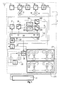
- Fig. 1 shows a schematic representation of a radio receiver, which consists of an RF part 1, a quadrature part 2 and an arrangement for digital signal processing 3.
- a received signal is frequency selected and converted to a carrier frequency.
- the signal received by an RF reception stage 11 is downmixed to a first intermediate frequency ZF1 by means of a first IF mixer 12, to which a first variable IF mixing frequency f zf1 is supplied by a first IF oscillator 13.
- the input signal mixed down to this first intermediate frequency is combined in one first IF amplifier 14 bandpass filtered and amplified and fed to a second IF mixer 15, in which the input signal is mixed down to a second intermediate frequency ZF2 by means of a second intermediate frequency supplied by a second IF oscillator 16.
- this second intermediate frequency ZF2 is in turn bandpass filtered and amplified.
- the second intermediate frequency ZF2 is fed to an analog / digital converter 21 in the quadrature part 2.
- This analog / digital converter 21 is controlled by a central clock 20 by means of clock pulses f i .
- the second intermediate frequency f IF2 was chosen so that it corresponds to an integer multiple of half the bit clock frequency f b .
- the value 79 was selected as an integer ratio of the second oscillator frequency f IF2 and half the bit clock f b .
- a clock generator 201 is arranged in a central clock controller 20 and generates a basic clock of a quarter of the wavelength of the second intermediate frequency f IF2 .
- Deviations from the intended frequency ratio between the second intermediate frequency ZF2 and the basic clock act like a frequency detuning. With appropriately designed downstream signal processing, such frequency detuning that is small in relation to the bandwidth of the signal can be tolerated. However, it is cheaper to avoid such frequency detuning from the outset shut down. It is particularly advantageous to also derive the mixed frequency of the second IF oscillator 16 from the clock generator 201. As a result, the frequency ratio of the second intermediate frequency ZF2 and the basic clock can be rigidly determined independently of external influences.
- 158 basic clock cycles correspond to exactly one bit cycle of the bit frequency f b .
- This basic cycle is fed to a counter 202.
- This counter 202 generates the sampling pulse f i at every ninth basic clock.
- two adjacent sample values are exactly 2 wavelengths apart from one another at the second intermediate frequency ZF2.
- the counter generates exactly seventeen such equidistantly consecutive scanning pulses within one bit clock. These seventeen successive samples thus form a group of equidistant samples.
- a possible sampling pulse at the 153rd basic clock is suppressed, so that exactly nine samples for the normal component and eight samples for the quadrature component are obtained in this way in each bit clock.
- the counter is reset after every 158 basic clocks and the clock generation of the sampling pulses f i is started again as described above. In this way, the sequence of the generated sampling pulses f i continues periodically after every 158th basic cycle.
- the group distance is chosen to be larger than the distance between two successive samples within a group.
- a correspondingly fast analog / digital converter is required however, the group distance can also be set to be smaller than the distance between two successive samples of a group.
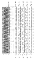
- FIG. 2a shows an unmodulated carrier vibration f c , a time axis being plotted in the lower part of FIG. 2a, in which each basic cycle is represented by a dash of the time axis.
- the time interval of the sampling pulses f i is selected such that this distance corresponds to exactly 2 wavelengths of the second intermediate frequency ZF2, sampling values of the normal and quadrature components are obtained alternately through these sampling pulses.
- the alternating successive samples of a bit clock period of the normal and quadrature components the component distributor 22, symbolically represented in the drawing as a switch, alternately assigned to a first signal branch for processing the normal component and a second signal branch for processing the quadrature component.
- a corresponding switching signal Q1 for controlling the component distributor 22 is also generated by the counter 202.
- the component distributor 22 is constructed in such a way that, at a low voltage level (low signal) at a switching input, it feeds the sample present at an input to the first signal branch for the processing of the normal component and at a switching signal with a high voltage level (high signal) forwarding the present sample to the second processing branch for processing the quadrature components.
- the voltage level curve of the switching signal Q1 controlling the component distributor 22 is shown in FIG. 2c. It can clearly be seen that the switching signal Q1, starting at the 0th basic clock, alternately changes its voltage level from low to high and vice versa with a low level every nine basic clocks. At the beginning of the next bit clock, in the exemplary embodiment and in FIG. 2a the basic clock number 158, the signal curve of the switching signal Q1 corresponds to that in the previous bit clock.
- a sign inverter 231, 232 and a changeover switch 233, 234 are provided in each signal branch. These change-over switches 233, 234 are constructed in such a way that their switches are at a low level The samples of the respective processing branch are directly switched through, while the samples of the sign inverters 231, 232 are passed on at a high level at their switching inputs.
- the course of a second switching signal Q2, which controls the first switch 233, is shown in FIG.
- FIG. 2e shows the loss of a third switching signal Q3, which controls the switching state of the second switch 234, is shown in FIG. 2e.
- the second and third switching signals Q2, Q3 also generated by the counter 202 are selected such that the sample value is alternately forwarded in each signal branch or the inverted sample value is forwarded for every second sample value.
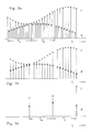
- 3a shows the sample values of a modulated signal obtained after the sign reversal, the normal components having an x at their apex and the quadrature components having an o at their apex. Although normal and quadrature components are processed in separate signal branches, they are always shown together in FIG. 3 in order to clarify their temporal assignment to one another. From FIG. 3a it can be seen that a sample of the quadrature component is time-controlled and lies in the middle between two samples of the normal component.
- the normal component is filtered in an interpolator 25. Since the sampling values used for the interpolation are equidistant and closely adjacent, the structure of the interpolator is simplified and the interpolation result is improved. In the exemplary embodiment, a linear interpolator is used, which in each case forms an interpolation value from two successive sample values.
- the last sample value is in each case in the interpolator 25 cached in a register.
- the temporarily stored sample value and the sample value currently present at the input are halved, for example by shifting the bit pattern to the left by one position, and then added.
- the value interpolated in this way corresponds to a good approximation to a sample value which would have been obtained in the middle between the two last sample values supplied to the interpolator.
- the interpolated sample of the normal component and the sample of the quadrature component, which was sampled in time between the two last samples of the normal component fed to the interpolator 25, are to be regarded as sampled at the same time.
- the associated sample value of the quadrature component must be delayed by a delay element 24.
- This time delay corresponds exactly to the distance between two regularly consecutive scanning pulses f i , that is to say 9 basic clocks in the exemplary embodiment.
- the interpolation produces eight interpolated samples from the nine samples of the normal component of a bit clock (see FIG. 3b).
- An off switch 26 controlled by a fourth control signal Q4 prevents an interpolated value formed after the ninth sample value from being passed on (see signal curve of the switching signal Q4 in FIG. 2e). Because of the delay in the output values of the interpolator due to the interpolation, the switching signal Q4 is generated with a time delay by precisely this delay.
- 3b shows how eight interpolated samples of the normal component are obtained from the nine samples of the normal component.
- the eight interpolated samples of the normal component and the eight samples of the quadrature component are each fed to an averaging filter 271, 2f2.
- filters 271, 272 a single value for the normal component or the quadrature component is formed from the respective eight sample values.
- the eight times oversampling in this way reduces the quantization noise of the analog / digital converter by nine dB. In this way, exactly one value for the normal component and the quadrature component is obtained for each bit clock.
- the equidistant spacing of the eight samples also simplifies the structure of the averaging filter.
- the sample values of a bit clock multiplied by a factor of 1/8 are summed up in order to obtain the mean value of the respective normal or quadrature component of a bit clock.
- 3c shows how a single averaged sample value is generated from eight sample values in each case, at the end of a bit clock.
- the number of basic clocks per bit clock is a number divisible without a remainder by four, the result of averaging successive bit clocks is correct and the quadrature components obtained in the above manner can be passed on for digital signal processing without revision. If, however, as in the present case, there remains a remainder of two when dividing the basic clocks per bit clock, then the quadrature compo obtained in the above manner must nents are inverted for every second bit clock. However, this can also be advantageously achieved in that the counter 201 generates the control signals for switching the changeover switches 231, 232 out of phase by 180 degrees in every second bit cycle (see in particular the course of the switching signals Q2, Q3 during the basic clocks 158 to 15).
- the switching signals Q2 and Q3 only continue periodically after every second bit interval, while the switching signals Q1 and Q4 each continue periodically after every bit interval.
- the quadrature components rotate by 90 degrees from bit clock to bit clock.
- the sample value of the normal component 1 becomes the quadrature component Q in the second bit cycle, the inverted normal component -I in the third bit cycle and the inverted quadrature component -Q in the fourth bit cycle.
- the number of basic clocks per bit clock is selected so that it divides by four to give a remainder of three, then the quadrature components lag behind by 90 degrees in phase from bit clock to bit clock.
- a nonlinear angle modulation such as a type of modulation known as gaussian minimum shift keying (GMSK) or a type of modulation known as generalized tamed frequency modulation (GTFM)
- GMSK gaussian minimum shift keying
- GTFM generalized tamed frequency modulation
- the counter 201 While maintaining the intervals of the scanning pulses fi, the counter 201 generates the same switching signals Q1, Q2, Q3 and Q4, an additional 159th basic clock being inserted per bit interval after every 158th basic clock, in which all switching signals Q1, Q2, Q3 maintain the same signal state as in the previous basic clock 158. Because of the rotation, the switching signals remain the same in the successive bit intervals and are repeated periodically after each bit interval T a .
- this rotation can be reversed by bit-by-bit swapping or and / or inverting the components be made. This can be done, for example, by postprocessing the quadrature components by feeding the quadrature components to a swap switch, not shown, which interchanges the normal component and quadrature component with one another in every second bit interval T a .
- the inversions still required can already be carried out by appropriately controlling the changeover switches 233, 234.
- the second intermediate frequency ZF2 is again selected such that a bit interval corresponds to 158 basic clocks, as in the first exemplary embodiment.
- the position of the sampling pulses and switching signals for four successive bit intervals are shown.
- the sampling pulses f i and switching signals of the first bit interval correspond to the sampling pulses and switching signals during the first bit interval in the first exemplary embodiment.
- the periodic continuation of the scanning pulses and the associated switching signals is delayed by one basic clock in three successive bit intervals and shortened by three basic clocks in a subsequent fourth bit interval.
- the scanning pulse sequence and the associated switching signals are again delayed by a basic clock.
- the first sample pulse of the fourth sample interval thus corresponds to the basic clock 477.
- the sample value obtained by the first sample pulse in the fourth bit interval thus corresponds to the sample value of a quadrature component and the second sample value of the fourth bit interval corresponds to an inverted sample value of the quadrature component.
- the periodic continuation of the scanning pulses and the switching signals Q1, Q2, Q3 is in each case one basic cycle longer than the number of basic cycles per interval, so in this exemplary embodiment it is 159 basic cycles three times in succession.
- the time interval between the first sample value of the fourth bit interval and the first sample value of the next bit interval is shortened by three basic clock cycles in this exemplary embodiment and is accordingly only 155 basic clock cycles.
- the first sample of the fifth bit interval lies at the basic clock 632.
- a sample of the normal component is obtained again by the first sampling pulse of the fifth bit interval.
- the course of the sampling pulses and the signal course of the fifth sampling interval now again corresponds to the first sampling interval.
- the sampling pulses are shifted in successive bit intervals T a by a quarter period of the second intermediate frequency ZF2.
- samples of the I and Q components are alternately fed to each of the two branches.
- I and Q components are interpolated alternately.
- This embodiment offers the advantage that the course of the switching signals Q1, Q2, Q3 remains the same in all four bit intervals. This simplifies the construction of the counter.
- the counter is reset three times in a row after 159 basic cycles and after these three longer basic cycles once already after 155 basic cycles.
- this embodiment can also be applied to versions in which the number of basic clock cycles per bit interval is an odd number, and the rotation effect of the sampling values that is caused thereby is to be reversed.
Landscapes
- Engineering & Computer Science (AREA)
- Computer Networks & Wireless Communication (AREA)
- Signal Processing (AREA)
- Digital Transmission Methods That Use Modulated Carrier Waves (AREA)
Applications Claiming Priority (2)
| Application Number | Priority Date | Filing Date | Title |
|---|---|---|---|
| DE3938126A DE3938126A1 (de) | 1989-11-16 | 1989-11-16 | Empfaenger mit direkter quadratur-abtastung des eingangssignals |
| DE3938126 | 1989-11-16 |
Publications (3)
| Publication Number | Publication Date |
|---|---|
| EP0428226A2 true EP0428226A2 (fr) | 1991-05-22 |
| EP0428226A3 EP0428226A3 (en) | 1993-01-13 |
| EP0428226B1 EP0428226B1 (fr) | 1996-09-04 |
Family
ID=6393664
Family Applications (1)
| Application Number | Title | Priority Date | Filing Date |
|---|---|---|---|
| EP90202997A Expired - Lifetime EP0428226B1 (fr) | 1989-11-16 | 1990-11-13 | Recépteur à échantillonage directe en quadrature du signal d'entrée |
Country Status (7)
| Country | Link |
|---|---|
| US (1) | US5142553A (fr) |
| EP (1) | EP0428226B1 (fr) |
| JP (1) | JP2991245B2 (fr) |
| KR (1) | KR0176696B1 (fr) |
| CA (1) | CA2029802C (fr) |
| DE (2) | DE3938126A1 (fr) |
| FI (1) | FI103159B (fr) |
Cited By (3)
| Publication number | Priority date | Publication date | Assignee | Title |
|---|---|---|---|---|
| EP0458452A3 (fr) * | 1990-05-25 | 1991-12-18 | Nokia Mobile Phones (U.K.) Limited | Démodulateur de quadrature |
| FR2691315A1 (fr) * | 1992-05-15 | 1993-11-19 | France Telecom | Dispositif numérique de génération de l'enveloppe complexe d'un signal de porteuses modulées en quadrature. |
| WO1998006206A1 (fr) * | 1996-08-07 | 1998-02-12 | Sat (Societe Anonyme De Telecommunications) | Demodulateur a circuit numerique de recuperation de porteuse et de rythme |
Families Citing this family (22)
| Publication number | Priority date | Publication date | Assignee | Title |
|---|---|---|---|---|
| JP3003826B2 (ja) * | 1992-12-11 | 2000-01-31 | 三菱電機株式会社 | クロック再生回路 |
| US5375146A (en) * | 1993-05-06 | 1994-12-20 | Comsat Corporation | Digital frequency conversion and tuning scheme for microwave radio receivers and transmitters |
| US5410499A (en) * | 1994-03-31 | 1995-04-25 | The United States Of America As Represented By The Secretary Of The Navy | Phase shifter for directly sampled bandpass signals |
| JP3055085B2 (ja) * | 1994-04-22 | 2000-06-19 | 株式会社アドバンテスト | デジタル変調解析装置 |
| JPH07321862A (ja) * | 1994-05-25 | 1995-12-08 | Matsushita Electric Ind Co Ltd | ディジタル変調波復調装置 |
| US5841814A (en) * | 1995-10-17 | 1998-11-24 | Paradyne Corporation | Sampling system for radio frequency receiver |
| US5937341A (en) | 1996-09-13 | 1999-08-10 | University Of Washington | Simplified high frequency tuner and tuning method |
| US6151354A (en) * | 1997-12-19 | 2000-11-21 | Rockwell Science Center | Multi-mode, multi-band, multi-user radio system architecture |
| FR2780590B1 (fr) * | 1998-06-29 | 2000-10-06 | Sgs Thomson Microelectronics | Demodulateur qpsk a entree en frequence intermediaire |
| US6624691B1 (en) | 1999-10-04 | 2003-09-23 | Nec Corporation | Demodulator for processing digital signal |
| DE10005497A1 (de) | 2000-02-08 | 2001-08-09 | Infineon Technologies Ag | Verfahren und Schaltungsanordnung zum Demodulieren eines quadraturamplituden- oder phasenmodulierten Signals |
| US7388931B1 (en) | 2002-06-12 | 2008-06-17 | Marvell International Ltd. | ADC architecture for wireless applications |
| US7272375B2 (en) | 2004-06-30 | 2007-09-18 | Silicon Laboratories Inc. | Integrated low-IF terrestrial audio broadcast receiver and associated method |
| GB0421930D0 (en) * | 2004-10-01 | 2004-11-03 | Nokia Corp | Signal receiver |
| US7714760B2 (en) * | 2008-06-27 | 2010-05-11 | Entropic Communications, Inc. | Apparatus and methods for direct quadrature sampling |
| GB0903157D0 (en) | 2009-02-25 | 2009-04-08 | Innovation Res & Technology Pl | Demodulation mixing |
| US20110043286A1 (en) * | 2009-08-18 | 2011-02-24 | Gerald Youngblood | Direct conversion receiver |
| US9264268B2 (en) | 2012-10-12 | 2016-02-16 | Innoventure L.P. | Periodic time segment sequence based decimation |
| US9484968B2 (en) | 2012-10-12 | 2016-11-01 | Innoventure L.P. | Post conversion mixing |
| US9490944B2 (en) | 2012-10-12 | 2016-11-08 | Innoventure L.P. | Phase sector based RF signal acquisition |
| US9484969B2 (en) | 2012-10-12 | 2016-11-01 | Innoventure L.P. | Delta-pi signal acquisition |
| US9225368B2 (en) | 2012-10-12 | 2015-12-29 | Innoventure L.P. | Periodic time segment sequence based signal generation |
Family Cites Families (8)
| Publication number | Priority date | Publication date | Assignee | Title |
|---|---|---|---|---|
| US4079329A (en) * | 1976-11-11 | 1978-03-14 | Harris Corporation | Signal demodulator including data normalization |
| US4412302A (en) * | 1980-12-15 | 1983-10-25 | Rca Corporation | Digital phase demodulation and correlation |
| JPS5923945A (ja) * | 1982-07-30 | 1984-02-07 | Toshiba Corp | 無線回線信号の検出方式 |
| US4733403A (en) * | 1986-05-12 | 1988-03-22 | Motorola, Inc. | Digital zero IF selectivity section |
| US4910752A (en) * | 1987-06-15 | 1990-03-20 | Motorola, Inc. | Low power digital receiver |
| US4779054A (en) * | 1987-08-17 | 1988-10-18 | General Electric Company | Digital inphase/quadrature product detector |
| DE3815055A1 (de) * | 1988-05-04 | 1989-11-16 | Standard Elektrik Lorenz Ag | Quadratur-empfaenger |
| DE3823374A1 (de) * | 1988-07-09 | 1990-01-18 | Philips Patentverwaltung | Vorrichtung zur entzerrung und demodulation winkelmodulierter datensignale |
-
1989
- 1989-11-16 DE DE3938126A patent/DE3938126A1/de not_active Withdrawn
-
1990
- 1990-11-13 DE DE59010483T patent/DE59010483D1/de not_active Expired - Fee Related
- 1990-11-13 EP EP90202997A patent/EP0428226B1/fr not_active Expired - Lifetime
- 1990-11-13 CA CA002029802A patent/CA2029802C/fr not_active Expired - Fee Related
- 1990-11-13 FI FI905607A patent/FI103159B/fi not_active IP Right Cessation
- 1990-11-13 US US07/613,346 patent/US5142553A/en not_active Expired - Fee Related
- 1990-11-15 JP JP2311234A patent/JP2991245B2/ja not_active Expired - Fee Related
- 1990-11-15 KR KR1019900018461A patent/KR0176696B1/ko not_active Expired - Fee Related
Cited By (4)
| Publication number | Priority date | Publication date | Assignee | Title |
|---|---|---|---|---|
| EP0458452A3 (fr) * | 1990-05-25 | 1991-12-18 | Nokia Mobile Phones (U.K.) Limited | Démodulateur de quadrature |
| FR2691315A1 (fr) * | 1992-05-15 | 1993-11-19 | France Telecom | Dispositif numérique de génération de l'enveloppe complexe d'un signal de porteuses modulées en quadrature. |
| WO1998006206A1 (fr) * | 1996-08-07 | 1998-02-12 | Sat (Societe Anonyme De Telecommunications) | Demodulateur a circuit numerique de recuperation de porteuse et de rythme |
| FR2752348A1 (fr) * | 1996-08-07 | 1998-02-13 | Telecommunications Sa | Demodulateur a circuit numerique de recuperation de porteuse et de rythme |
Also Published As
| Publication number | Publication date |
|---|---|
| KR0176696B1 (ko) | 1999-05-15 |
| JPH03293843A (ja) | 1991-12-25 |
| FI905607A0 (fi) | 1990-11-13 |
| DE3938126A1 (de) | 1991-05-23 |
| FI905607A7 (fi) | 1991-05-17 |
| FI103159B1 (fi) | 1999-04-30 |
| JP2991245B2 (ja) | 1999-12-20 |
| FI103159B (fi) | 1999-04-30 |
| EP0428226B1 (fr) | 1996-09-04 |
| EP0428226A3 (en) | 1993-01-13 |
| CA2029802C (fr) | 2000-12-12 |
| CA2029802A1 (fr) | 1991-05-17 |
| DE59010483D1 (de) | 1996-10-10 |
| US5142553A (en) | 1992-08-25 |
| KR910010931A (ko) | 1991-06-29 |
Similar Documents
| Publication | Publication Date | Title |
|---|---|---|
| EP0428226B1 (fr) | Recépteur à échantillonage directe en quadrature du signal d'entrée | |
| EP0080014B1 (fr) | Démodulateur numérique pour signaux modulés en fréquence | |
| DE69524394T2 (de) | Entschachtelung und pufferung in einem speicher | |
| DE69326140T2 (de) | Psk empfänger | |
| DE69107248T2 (de) | Sender mit einer elektronischen Anordnung zum Erzeugen eines modulierten Trägersignals. | |
| AT397895B (de) | Digitales verzögerungsfilter | |
| DE69616022T2 (de) | Frequenzsynthetisierer | |
| DE2628581C3 (de) | Schaltung zur Wiedergewinnung von Taktsignalen mit veränderlicher Frequenz für einen Digitaldatenempfänger | |
| DE4200816A1 (de) | Frequenz- und phasenmodulator fuer digitale modulatoren bzw. digitale uebertragung, insbesondere fuer funkuebertragung | |
| DE2459751C3 (de) | Schaltungsanordnung zum Erzeugen von Signalen mit zunehmender Frequenz und von Signalen mit abnehmender Frequenz | |
| DE69101250T2 (de) | Digitale Phasendetektor-Anordnung. | |
| DE2541292C2 (de) | Vorrichtung zur Korrelierung von Signalen bei Dopplerradaranlagen zur Entfernungsmessung | |
| DE69003564T2 (de) | Wellenformengenerator. | |
| EP0324897A1 (fr) | Système de radar à dispositif expanseur numérique | |
| WO1986005594A1 (fr) | Circuit d'obtention d'une valeur moyenne | |
| EP0360349B1 (fr) | Générateur de fréquence numérique | |
| DE3919530C2 (fr) | ||
| EP0541878B1 (fr) | Convertisseur analogique/numérique Delta-Sigma | |
| DE3433592C2 (fr) | ||
| EP1472844B1 (fr) | Commande d'horloge et conversion de la frequence d'echantillonage dans l'emetteur d'un emetteur-recepteur numerique | |
| EP0497416B1 (fr) | Circuit pour la transformation de la base de temps d'un signal d'image numérique | |
| EP0002811B2 (fr) | Dispositif de thérapie par courants interférenciels | |
| DE2305094A1 (de) | Verfahren und system zur breitbandigen nachrichtenuebertragung | |
| DE3435032C2 (fr) | ||
| DE19729476C2 (de) | Numerisch gesteuerter Oszillator |
Legal Events
| Date | Code | Title | Description |
|---|---|---|---|
| PUAI | Public reference made under article 153(3) epc to a published international application that has entered the european phase |
Free format text: ORIGINAL CODE: 0009012 |
|
| AK | Designated contracting states |
Kind code of ref document: A2 Designated state(s): DE FR GB IT SE |
|
| PUAL | Search report despatched |
Free format text: ORIGINAL CODE: 0009013 |
|
| AK | Designated contracting states |
Kind code of ref document: A3 Designated state(s): DE FR GB IT SE |
|
| 17P | Request for examination filed |
Effective date: 19930701 |
|
| 17Q | First examination report despatched |
Effective date: 19950215 |
|
| GRAH | Despatch of communication of intention to grant a patent |
Free format text: ORIGINAL CODE: EPIDOS IGRA |
|
| GRAH | Despatch of communication of intention to grant a patent |
Free format text: ORIGINAL CODE: EPIDOS IGRA |
|
| GRAA | (expected) grant |
Free format text: ORIGINAL CODE: 0009210 |
|
| AK | Designated contracting states |
Kind code of ref document: B1 Designated state(s): DE FR GB IT SE |
|
| REF | Corresponds to: |
Ref document number: 59010483 Country of ref document: DE Date of ref document: 19961010 |
|
| ITF | It: translation for a ep patent filed | ||
| GBT | Gb: translation of ep patent filed (gb section 77(6)(a)/1977) |
Effective date: 19961120 |
|
| ET | Fr: translation filed | ||
| PLBE | No opposition filed within time limit |
Free format text: ORIGINAL CODE: 0009261 |
|
| STAA | Information on the status of an ep patent application or granted ep patent |
Free format text: STATUS: NO OPPOSITION FILED WITHIN TIME LIMIT |
|
| 26N | No opposition filed | ||
| REG | Reference to a national code |
Ref country code: FR Ref legal event code: CD |
|
| REG | Reference to a national code |
Ref country code: GB Ref legal event code: IF02 |
|
| REG | Reference to a national code |
Ref country code: GB Ref legal event code: 746 Effective date: 20020917 |
|
| REG | Reference to a national code |
Ref country code: FR Ref legal event code: D6 |
|
| PGFP | Annual fee paid to national office [announced via postgrant information from national office to epo] |
Ref country code: SE Payment date: 20031126 Year of fee payment: 14 Ref country code: FR Payment date: 20031126 Year of fee payment: 14 |
|
| PGFP | Annual fee paid to national office [announced via postgrant information from national office to epo] |
Ref country code: GB Payment date: 20031128 Year of fee payment: 14 |
|
| PGFP | Annual fee paid to national office [announced via postgrant information from national office to epo] |
Ref country code: DE Payment date: 20040121 Year of fee payment: 14 |
|
| PG25 | Lapsed in a contracting state [announced via postgrant information from national office to epo] |
Ref country code: GB Free format text: LAPSE BECAUSE OF NON-PAYMENT OF DUE FEES Effective date: 20041113 |
|
| PG25 | Lapsed in a contracting state [announced via postgrant information from national office to epo] |
Ref country code: SE Free format text: LAPSE BECAUSE OF NON-PAYMENT OF DUE FEES Effective date: 20041114 |
|
| PG25 | Lapsed in a contracting state [announced via postgrant information from national office to epo] |
Ref country code: DE Free format text: LAPSE BECAUSE OF NON-PAYMENT OF DUE FEES Effective date: 20050601 |
|
| EUG | Se: european patent has lapsed | ||
| GBPC | Gb: european patent ceased through non-payment of renewal fee |
Effective date: 20041113 |
|
| PG25 | Lapsed in a contracting state [announced via postgrant information from national office to epo] |
Ref country code: FR Free format text: LAPSE BECAUSE OF NON-PAYMENT OF DUE FEES Effective date: 20050729 |
|
| REG | Reference to a national code |
Ref country code: FR Ref legal event code: ST |
|
| PG25 | Lapsed in a contracting state [announced via postgrant information from national office to epo] |
Ref country code: IT Free format text: LAPSE BECAUSE OF NON-PAYMENT OF DUE FEES;WARNING: LAPSES OF ITALIAN PATENTS WITH EFFECTIVE DATE BEFORE 2007 MAY HAVE OCCURRED AT ANY TIME BEFORE 2007. THE CORRECT EFFECTIVE DATE MAY BE DIFFERENT FROM THE ONE RECORDED. Effective date: 20051113 |