EP0428715B1 - Systeme de detection et de mesure d'une bande optique, adapte notamment pour commander la generation de substances chimiques de traitement de films radiographiques - Google Patents
Systeme de detection et de mesure d'une bande optique, adapte notamment pour commander la generation de substances chimiques de traitement de films radiographiques Download PDFInfo
- Publication number
- EP0428715B1 EP0428715B1 EP90910060A EP90910060A EP0428715B1 EP 0428715 B1 EP0428715 B1 EP 0428715B1 EP 90910060 A EP90910060 A EP 90910060A EP 90910060 A EP90910060 A EP 90910060A EP 0428715 B1 EP0428715 B1 EP 0428715B1
- Authority
- EP
- European Patent Office
- Prior art keywords
- web
- intensity
- photodetectors
- array
- level
- Prior art date
- Legal status (The legal status is an assumption and is not a legal conclusion. Google has not performed a legal analysis and makes no representation as to the accuracy of the status listed.)
- Expired - Lifetime
Links
- 238000001514 detection method Methods 0.000 title claims abstract description 18
- 239000000126 substance Substances 0.000 title claims abstract description 11
- 238000012545 processing Methods 0.000 title claims description 8
- 238000005259 measurement Methods 0.000 title description 12
- 230000003287 optical effect Effects 0.000 title description 10
- 238000005286 illumination Methods 0.000 claims abstract description 25
- 238000003491 array Methods 0.000 claims abstract description 8
- 239000003990 capacitor Substances 0.000 claims description 8
- 230000003247 decreasing effect Effects 0.000 claims description 8
- 239000011159 matrix material Substances 0.000 claims description 4
- 238000005070 sampling Methods 0.000 claims description 4
- 238000010586 diagram Methods 0.000 description 6
- 230000002411 adverse Effects 0.000 description 3
- 230000007423 decrease Effects 0.000 description 2
- 239000000428 dust Substances 0.000 description 2
- 238000005516 engineering process Methods 0.000 description 2
- 238000012360 testing method Methods 0.000 description 2
- 238000005406 washing Methods 0.000 description 2
- 230000032683 aging Effects 0.000 description 1
- 230000003321 amplification Effects 0.000 description 1
- 238000006243 chemical reaction Methods 0.000 description 1
- 230000003292 diminished effect Effects 0.000 description 1
- 238000007599 discharging Methods 0.000 description 1
- 238000006073 displacement reaction Methods 0.000 description 1
- 230000000694 effects Effects 0.000 description 1
- 230000007613 environmental effect Effects 0.000 description 1
- 239000000835 fiber Substances 0.000 description 1
- 238000002955 isolation Methods 0.000 description 1
- 238000012423 maintenance Methods 0.000 description 1
- 238000000034 method Methods 0.000 description 1
- 238000012986 modification Methods 0.000 description 1
- 230000004048 modification Effects 0.000 description 1
- 238000003199 nucleic acid amplification method Methods 0.000 description 1
- 230000002035 prolonged effect Effects 0.000 description 1
- 230000004044 response Effects 0.000 description 1
- 238000011144 upstream manufacturing Methods 0.000 description 1
Images


Classifications
-
- G—PHYSICS
- G03—PHOTOGRAPHY; CINEMATOGRAPHY; ANALOGOUS TECHNIQUES USING WAVES OTHER THAN OPTICAL WAVES; ELECTROGRAPHY; HOLOGRAPHY
- G03D—APPARATUS FOR PROCESSING EXPOSED PHOTOGRAPHIC MATERIALS; ACCESSORIES THEREFOR
- G03D3/00—Liquid processing apparatus involving immersion; Washing apparatus involving immersion
- G03D3/02—Details of liquid circulation
- G03D3/06—Liquid supply; Liquid circulation outside tanks
- G03D3/065—Liquid supply; Liquid circulation outside tanks replenishment or recovery apparatus
-
- G—PHYSICS
- G01—MEASURING; TESTING
- G01N—INVESTIGATING OR ANALYSING MATERIALS BY DETERMINING THEIR CHEMICAL OR PHYSICAL PROPERTIES
- G01N21/00—Investigating or analysing materials by the use of optical means, i.e. using sub-millimetre waves, infrared, visible or ultraviolet light
- G01N21/84—Systems specially adapted for particular applications
- G01N21/88—Investigating the presence of flaws or contamination
- G01N21/89—Investigating the presence of flaws or contamination in moving material, e.g. running paper or textiles
- G01N21/8901—Optical details; Scanning details
- G01N21/8903—Optical details; Scanning details using a multiple detector array
Definitions
- the present invention relates to optical web detection systems utilizing arrays of light emitting sources and photodetectors, between which a web passes, for detecting the presence and the dimensions, including area, of the web.
- the invention relates more particularly to a system for controlling the illumination from the light emitting sources so as to ensure that even semi-opaque (low density) webs may be detected and to ensure uniformity and amount of illumination that does not adversely affect the web, such as by fogging photo-sensitive webs.
- the invention is especially suitable for use in equipment for processing (developing) radiographic film such as X-ray film by detecting the film entering the processor and measuring its area using an array of infrared light emitting diodes (LED) as the light emitting sources and infrared photodetectors as optical detectors; the film area being measured by the system and used to control the replenishment of chemicals needed to maintain proper chemical activity for processing of the film.
- equipment for processing developing radiographic film
- LED infrared light emitting diodes
- Optical detection techniques have been used to sense the presence of media, but not in real time as film is being processed.
- a sensor system for detecting dust in the light path from a light emitting diode (LED) to a phototransistor when media is absent from the path.
- the system increases current to the LED for increasing light which is detected by the phototransistor.
- a reference voltage to a comparator is increased.
- the comparator does not detect a sufficiently high light output in spite of increases in the current to the light emitting device, an alarm is given so that the path can be cleared of dust when media is later inserted.
- Web (film) detection and measurement devices using arrays of light emitting diodes and photodetectors have heretofore been used for controlling the replenishment of chemicals in film processing apparatus, as for example, described in EP-A-0 037 561 and in DE-A-31 42 881.
- Such equipment as has heretofore been available has not been completely satisfactory due to variability of the light output across the array.
- the brightness of light (intensity) produced by the LEDs can vary from LED to LED. LED output also decreases with age and can be affected by dirt and temperature variations. Where light pipes or fibers are used to direct beams of light from the LEDs, they tend to further increase the variability in light output as seen by the web.
- Ultrasonic detectors are more expensive than optical detectors and tend to be unreliable even when shielded against outside noise and vibration.
- the system embodying the invention which provides for web detection and measurement and which is operable on semi-opaque webs, such as X-ray films, embodies an array of light emitting sources disposed in a direction which is across the web and an array of optical detectors in receptive relationship from light from the sources.
- web as used herein includes continuous webs as well as sheets.
- Computer controlled means are provided for setting the intensity of light from each of the sources to a preset level, such that the interposition of a web between any of the sources and the detectors which are in light receiving relationship therewith will reduce the intensity of light incident on the detector below a certain threshold even when the web is semi-opaque.
- the computer controlled means are operative during operation of the system in the absence of any web between the sources and detector arrays and is responsive to electrical signals from the detectors, for incrementally increasing and decreasing the preset levels when the level of light received by the detectors is below and above this preset level, respectively, thereby maintaining the level of illumination uniform and at the preset level.
- the signals obtained when a detector is blocked by the web are utilized for measurement of the width and/or area of the web and to control the replenishment of chemicals when the detection system is used in a film processor.
- the signal obtained when a detector is blocked is also used to incrementally increase and decrease the preset levels to prevent the LED output from fluctuating when the web is present for extended periods.
- a X-ray film processor in which X-ray films, usually sheets, from an X-ray camera as used in the radiology department of a hospital or the office of a radiologist is processed.
- the processor has tanks 100, 102 and 104 for developing, fixing and washing of the film. After washing the film is dried in a dryer 106.
- Guide and drive rolls 108 which are driven by motors through suitable gearing or chain and sprocket arrangements advance the film through the tanks 100, 102 and 104 and through the dryer 106.
- a film detector and measurement system is disposed upstream in the direction of travel of the film from the processor tanks 100, 102 and 104 this system is referred to as a universal film detector or UFD 110.
- the UFD 110 computes the area of film which has passed through it. Then it operates a motor control, such as a relay 116.
- the relay turns on the motor of pumps, suitably positive displacement pumps 118 (PDP), for an interval of time sufficient to meter enough chemicals (developer and fixer) from supply tanks 120 and 122 to replenish the chemistry in the fixer and developer tanks 100 and 102.
- PDP positive displacement pumps 118
- the pumps are turned on for a fixed period of time, for example 10 seconds which will be enough to meter sufficient developer and fixer for processing a certain area of film, for example 14 x 17 inch sheet of film.
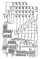
- the UFD contains a housing 200 in which is mounted a printed circuit board 202.
- the housing and board have aligned slots (slot 204 on the board 202 being shown in FIG. 2) through which the film passes.
- On the board is a linear array of infrared LEDs (e.g., twenty-two LEDs) which are equally spaced from each other along the slot 204.
- Opposite to the LEDs is an array of photodetectors. Twenty-two photodetectors may be used each corresponding to a different one of the LEDs and each in light receptive relationship therewith (aligned with its corresponding LED).
- an aperture plate 206 is disposed between the LED array and the slot 204.
- This aperture plate has twenty-two apertures 208 each aligned with a different LED.
- Components such as computer chips, resistors, and capacitors of the UFD are mounted on the board 202 and connected by printed wiring (not shown) to the LEDs and photodetectors.
- FIG. 3 there is shown the slot 204 and the board 202 with the aligned LEDs and photodetectors in their respective arrays.
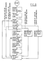
- the system is controlled by a microprocessor, for example, Motorola type MC68HC11 which has a built-in analog digital converter (A/D).
- the microprocessor 300 via a multiplexer 302, applied sequentially to the LEDs operating currents so that they illuminate (emit light pulses) sequentially and successively scan the slot 204 and any film therein.
- the current through the LEDs and therefore the intensity or brightness of illumination is controlled by the microprocessor which outputs a digital value to a digital to analog converter (D/A) 304.
- the analog output from the D/A 304 operates an intensity control circuit 306 which is a variable amplifier or current sink described more fully in connection with FIGS. 5 and 6.
- the brightness from the LEDs is made uniform from LED to LED and at a preset level.
- the setting of the brightness utilizes signals from the photodetectors which are combined in a combining and amplification network 308.
- This network provides an analog signal to a peak detector.
- the peak detector is enabled by the microprocessor 300 and provides output pulses corresponding in amplitude to the intensity of illumination detected by the network 308. These pulses are outputted by the peak detector 310 to the A/D input of the microprocessor 300.
- the microprocessor controls or recalibrates the LEDs so as to maintain the uniform intensity of illumination in spite of aging, dirt or other environmental effects.
- the level of illumination is such that even low density or semi-opaque films in the slot 204 are detected without using an intensity of illumination which might adversely affect (fog) the film.
- a series of pulses below a preset threshold are detected. These pulses are counted and used to compute the area of the film passing through the slot. The output is applied to the replenishment motor pump control 116 (FIG. 1).
- the system shown in FIG. 3 operates on a sequential or serial basis to successively scan the slot. It also operates with pulses or flashes of illumination thereby further reducing the possibility of adverse affect on any film in the slot 204 by excessive illumination.
- pulse trains (a) and (b) which are applied to the multiplexer 302. These pulses are relatively short, for example, 25 microseconds, and are applied to successively enable the LEDs with 11 milliseconds (ms) between pulses. Pulses in train (a) are column enabling pulses while pulses in train (b) are row enabling pulses. Simultaneous occurrence of the pulses enables the multiplexer to allow passage of current through the intensity control or current sink 306 (see FIG. 5).
- the current level is represented by the output signals from the D/A as the pulses in train (c). Upon simultaneous occurrence of these pulses, a particular LED is turned on. After a sequence of twenty-two of these pulses (there being 22 LEDs as shown in FIG. 2) a scan is completed. It has been found that with short pulses of 25 microsecond duration with 11 milliseconds between pulses, a scan requires approximately 233 milliseconds. Scanning goes on continuously during run time, while the processor is on and ready to process film.
- the microprocessor outputs the RST/TRACK control level to the peak detector 310. This level is shown in (d). Prior to the predetermined period when LED is turned on, the control signal switches from reset (RST) to track level and enables the peak detector to see and track the amplitude of the pulses. The pulse which is tracked will correspond to the LED which is illuminated. At the end of the track interval, the microprocessor reads the signal from the peak detector. Then, the RST/TRACK signal reverts to the RST level which readies the peak detector (by discharging a storage capacitor 602 (FIG. 7)) so as to be ready for the next pulse from the next photodetector.
- RST reset
- the microprocessor has manual controls and provides outputs to a LED display (not shown) on the board 202 (FIG. 2).
- the controls which may be actuated by push buttons, are called the accumulator test controls. Diagnostics such as application of certain currents to the LEDs may be enabled upon accumulator test to determine if the LEDs are operating, for example, with a predetermined output level as measured by the microprocessor from the peak detector analog signal output in response to a certain current as presented to an LED via the D/A converter 304.
- the replenish set sets the time duration during which the replenish pump will be run (see FIG. 1), for example, to meter chemicals for a 14 x 17 inch film area.
- the transport speed set sets the measurement computation in accordance with the speed at which the film is driven through the processor. This speed may be varied by the processor's motor controllers, by gear changes in the film drive, or the like.
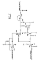
- the matrix multiplexer (MUX) 302 effectively provides column and row pulses for sequentially enabling pulses of current from +12V (the power supply) through column transistor switches 400 and row transistor switches 402. Only one of the 22 LEDs is illustrated in the multiplexer in FIG. 5. The matrix of rows and columns of the 22 LEDs is shown in FIG. 6. The first row and column transistors 400 & 402 (column 0 and row 0) are shown in FIG. 5. The microprocessor outputs digital signals which switch these transistors on and off through level shifters 404 and 406. It will be apparent that the LEDs are enabled in sequence by the four-bit and six-bit digital signals from the microprocessor 300 which are applied to the level shifters 404 and 406 to shift the voltage levels for operation of these transistors.
- the sequence of enablement is in the order stated, i.e., LED 1 followed by LED 2 followed by LED 3. . . through LED 22, which completes a scan and then back to LED 1 and so forth.
- the current path is not completed until the current sink 306 is operated.
- the current sink 306 is provided by an operational amplifier 318 which receives the analog signal from the D/A 304.
- the signal level, and therefore the current level is determined by an 8-bit digital signal (D-out) and therefore has 256 (0 to 255) increments.
- the current level is therefore controllable in 256 increments in this illustrative embodiment by controlling the current through the current sink transistor 410.
- an enabling analog signal to the current sink 306 an LED (1 through 22) will be illuminated at certain level of illumination (1 of 256 levels) as determined by the D-OUT digital value.
- the photodetectors are, as shown in FIG. 5, connected together in groups. Their output signals are applied through transimpedence (current to voltage conversion) amplifiers 412 which provide output voltages (an analog signal shown in FIG. 5 by the legend ANALOG SIG IN) through isolation diodes 414. The signal amplitude is controlled by a voltage divider 416 and applied to the peak detector 310.
- ANALOG SIG IN is buffered in an amplifier 710 and applied to a first switch in the form of an FET 712 which is in series with the storage capacitor 602. Another FET 714 is connected and parallel with the storage capacitor 602.
- the RST/TRACK control signal is applied to the series FED switch 712 through a transistor driver 716, and to the parallel FET 714 through an inverting transistor 718. Accordingly, during the reset time the peak detector is reset by discharge of the capacitor 602.
- the output signal (ANALOG SIG OUT) is derived from a buffer amplifier 720 and applied to the A/D input of the microprocessor 300.
- D/A values (the values of the D-OUT signal) which will obtain a certain level of intensity from each of the 22 LEDs is stored in the memory of the computer.
- This D-OUT value may vary from LED to LED. For example, it may correspond to 45 for the first LED, 30 for the second LED, 60 for the third LED, out of a scale of 1 to 255; 255 being the maximum output.
- the uniformity of intensity is measured by way of ANALOG SIG OUT.
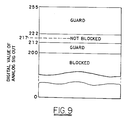
- the values of the corresponding 8-bit binary signal digitized by the A/D input of the microprocessor 300, as shown in FIG. 9. The selected value, for example, is 217.
- This is in a range from 212 to 222 and is desirably in the center of the range.
- the level of intensity is such that the least dense or most transparent (semi-opaque) film when present will produce an ANALOG SIG OUT which in digital value is in the blocked range of from 0 to 200 and preferably in the middle of that range, approximately 100.
- guard ranges above and below the predetermined level of 217 there are guard ranges above and below the predetermined level of 217.
- the lower guard range is from 200 to 212 while the upper guard range is from 222 to 255.
- the system is ready to run. Now the microprocessor points to and enables the first LED.
- the ANALOG SIG OUT is read by the computer.
- the computer classifies this output in accordance with its value as to whether or not the value lies in the blocked region (0-200).
- a counter in the microprocessor is incremented. This is an area counter.
- a certain count is detected which corresponds to a certain area of film, in this embodiment the area is 14 x 17 inches. In other words, an area of film is measured depending upon the number of LEDs blocked by the film region in the slot 204 (FIGS. 2 and 3). If the count is equal to or greater than that corresponding to the 14 x 17 inch sheet, the motor control is activated and the replenish pump is turned on for a predetermined period of time. Then the area counter is reset. After this computation the system points to the next LED.
- a recalibration program is executed which classifies the ANALOG SIG OUT value in terms of its corresponding A/D value from 0 to 255. If film is interposed between the LED and photodiode, the A/D value is compared to the first reading that indicated film was present. If the A/D value is greater than the stored reading, then the D to A value which was stored in the microprocessor memory is decremented by one (1 out of 256 on an 8-bit binary scale). If the A/D value is less than the stored reading then the D to A will be incremented by one.
- A/D values for each LED during a scan is classified as to whether no value lies in the not blocked region (corresponding to 212 to 222 - see FIG. 9) or in the upper or lower guard regions. If in the upper guard region, the illumination is too intense. Then the D to A value which was stored in the microprocessor memory is decremented by one (1 out of 256 on an 8-bit binary scale). If the value is detected to be in the lower guard region (from 200 to 212), the intensity is too low and the stored D to A value for the LED which is enabled is incremented by one. The successive incrementing and decrementing of the stored values recalibrates the system so that the intensity of illumination remains uniform and substantially constant during the run mode. Such constant illumination at the requisite level assures detection even of semi-opaque film.
Landscapes
- Physics & Mathematics (AREA)
- General Physics & Mathematics (AREA)
- Photographic Processing Devices Using Wet Methods (AREA)
- Investigating Or Analysing Materials By Optical Means (AREA)
- Geophysics And Detection Of Objects (AREA)
- Controlling Sheets Or Webs (AREA)
Abstract
Claims (18)
- Système (110) pour la détection et la mesure de bande, pouvant être mis en oeuvre sur des bandes semi-opaques photosensibles telles que des films pour rayon X, ledit système comprenant :
un réseau de sources émettant de la lumière disposé dans une direction qui est transversale à la bande,
un réseau de détecteurs photo-électriques en relation de réception de la lumière provenant desdites sources du réseau, caractérisé par
des moyens (300, 302, 304, 306) pour préétablir l'intensité de la lumière provenant de chacune desdites sources à un premier niveau (217) de sorte que l'interposition d'une bande entre l'une quelconque desdites sources et desdits détecteurs photo-électriques en relation de réception de la lumière avec celle-ci diminuera l'intensité de la lumière tombant sur ce détecteur photoélectrique au-dessous d'un certain seuil (200) même lorsque ladite bande est semi-opaque, et
des moyens (300, 302, 304, 306, 310) mis en oeuvre pendant l'opération de détection de bande dudit système et répondant aux signaux provenant des détecteurs photo-électriques pour accroître ou décroître par incrément lesdits premiers niveaux préétablis lorsque le niveau de signal desdits détecteurs photo-électriques correspond à une intensité de lumière laquelle est respectivement au-dessus ou au-dessous dudit premier niveau préétabli (217) de façon à obtenir un premier niveau corrigé d'intensité pour chacune desdites sources. - Système selon la revendication 1, dans lequel lesdits moyens pour décroître par incrément ladite intensité comportent des moyens (300, 310), répondant auxdits signaux lorsqu'ils correspondent à une première plage (222 à 250) d'intensité au-dessus dudit premier niveau pour diminuer ledit premier niveau, par un certain incrément d'intensité correspondant à moins de 1 % de la variation en amplitude desdits signaux entre l'amplitude lorsque lesdits détecteurs photo-électriques ne sont pas éclairés et lorsqu'ils sont éclairés à l'extrémité supérieure de ladite première plage.
- Système selon la revendication 2, dans lequel lesdits moyens pour accroître par incrément ladite intensité comportent des moyens (300, 310) répondant auxdits signaux lorsqu'ils correspondent à une seconde plage (200 à 212) de l'intensité au-dessous dudit premier niveau pour accroître ledit premier niveau par ledit certain incrément.
- Système selon la revendication 3, dans lequel lesdites première et seconde plages sont séparées l'une de l'autre par une plage donnée (212 à 222) d'intensité qui comporte ledit premier niveau approximativement au centre de celle-ci.
- Système selon la revendication 4 comprenant de plus des moyens (300, 308, 310) mis en oeuvre pour détecter l'interposition d'une bande entre ledit réseau de sources et ledit réseau de détecteurs photo-électriques lorsque lesdits détecteurs photo-électriques délivrent des signaux correspondant à l'intensité de lumière au-dessous de ladite seconde plage.
- Système selon la revendication 1 comprenant de plus des moyens (300, 302, 308, 310) répondant auxdits signaux correspondant à l'intensité d'éclairement desdits détecteurs photo-électriques à un niveau au-dessous dudit certain seuil pour mesurer la surface de ladite bande.
- Système selon la revendication 6 comprenant de plus des moyens (100, 102) pour traiter chimiquement ladite bande disposée en aval dudit réseau dans la direction de déplacement de ladite bande et des moyens (116, 118, 120, 122) pour délivrer des produits chimiques frais auxdits moyens de traitement lorsqu'une surface prédéterminée de ladite bande est mesurée.
- Système selon la revendication 1 comprenant de plus un boîtier comportant une fente (112, 204) à travers celui-ci pour le passage de ladite bande, au moins une carte de circuit (202) montée sur ledit boîtier (200) avec des parties sur les côtés opposés de ladite fente, ledit réseau de détecteurs photo-électriques et ledit réseau de sources étant chacun un réseau linéaire de dispositifs séparés disposés sur ladite carte sur des côtés opposés de ladite fente, lesdits dispositifs de sources et lesdits dispositifs détecteurs photo-électriques étant en alignement de sorte qu'un dispositif de sources différent parmi lesdits dispositifs de sources est opposé à un dispositif détecteur différent parmi lesdits dispositifs détecteurs photo-électriques, une plaque à ouverture (206) disposée sur un côté desdits côtés opposés contigus auxdits dispositifs de sources, ladite plaque à ouverture comportant une pluralité d'ouvertures (208) chacune alignée avec un dispositif de source différent parmi lesdits dispositifs de sources.
- Système selon la revendication 8, dans lequel lesdits dispositifs de sources sont des diodes électroluminescentes (DEL) et lesdits dispositifs détecteurs photo-électriques sont des photodiodes (PD).
- Système selon la revendication 1, dans lequel chacune desdites sources émettant de la lumière correspond à un détecteur photoélectrique différent parmi lesdits détecteurs photo-électriques et la lumière émise est d'une intensité correspondant au courant à travers celui-ci, comprenant de plus un ordinateur (300) et des moyens (302, 304, 306, 310) commandés par ledit ordinateur pour autoriser le passage de niveaux de courant prédéterminés se déplaçant à travers des sources successives desdits sources dans ledit réseau durant des intervalles de temps prédéterminés, balayant ainsi à travers ladite bande, lesdits moyens d'ordinateur et de commande commandant ledit moyen de préétablissement, des moyens commandés par ledit ordinateur pour échantillonner lesdits détecteurs photo-électriques pendant chacun desdits intervalles de temps prédéterminés pour délivrer lesdits signaux à partir des détecteurs photo-électriques successifs parmi lesdits détecteurs photo-électriques et ledit ordinateur comportant un moyen pour augmenter et diminuer par incrément le courant dans lesdites sources pour maintenir ledit premier niveau d'intensité.
- Système selon la revendication 10, dans lequel lesdits moyens commandés par ordinateur comprennent des moyens (304, 306) connectés en commun à la totalité desdites sources et répondant aux signaux numériques délivrés par ledit ordinateur pour commander ledit courant pendant lesdits intervalles de temps prédéterminés et des moyens de multiplexage (302) connectés audit ordinateur pour permettre successivement le passage d'un tel courant à travers lesdites sources émettant de la lumière.
- Système selon la revendication 10, dans lequel lesdites sources émettant de la lumière sont des photodiodes disposées en une matrice de rangées et de colonnes et lesdits moyens de multiplexage comprennent des moyens de commutation (402, 404) constitués desdites rangées et colonnes de diodes pour permettre le passage dudit courant à travers les diodes successives parmi lesdites diodes et ensuite à travers ledit moyen de commande de courant commun (306, 318, 410).
- Système selon la revendication 12, dans lequel ledit moyen d'échantillonnage commandé par ordinateur comprend un détecteur de crêtes (310) relié en commun à la totalité desdites photodiodes, des moyens mis en oeuvre par ledit ordinateur pour actionner ledit détecteur de crêtes afin d'échantillonner lesdits signaux pendant lesdits intervalles de temps prédéterminés et des moyens inclus dans ledit ordinateur pour numériser lesdits échantillons desdits signaux.
- Système selon la revendication 13, dans lequel lesdits moyens d'échantillonnage comprennent des premier (712) et second (714) interrupteurs, un condensateur (602) relié en série audit premier interrupteur et en parallèle audit second interrupteur, un moyen pour fermer ledit premier interrupteur et ouvrir ledit second interrupteur immédiatement avant chaque intervalle de temps prédéterminé pour fermer ledit second interrupteur et ouvrir ledit premier interrupteur entre chacun des intervalles de temps prédéterminés de manière à décharger ce condensateur et permettre la détection de crêtes du signal à partir de la photodiode immédiatement suivante.
- Système selon la revendication 1 comprenant de plus des moyens (302 ; 404, 406) pour allumer successivement lesdites sources d'émission de lumière dans ledit réseau pour balayer ladite bande et des moyens (300) pour mettre en oeuvre ledit moyen d'incrémentation ou de décrémentation chaque énième balayage ou N est de l'ordre de 10.
- Système selon la revendication 1, dans lequel lesdits moyens pour incrémenter et décrémenter comportent des moyens mis en oeuvre en l'absence de toute bande quelconque entre les réseaux de sources et de détecteurs photo-électriques.
- Système selon la revendication 16, dans lequel lesdits moyens pour incrémenter et décrémenter sont également fonctionnels lorsque la bande est présente entre les réseaux de sources et de détecteurs photo-électriques.
- Système selon la revendication 10 comprenant de plus des moyens (300, 302 ; 404, 406) pour mettre en oeuvre lesdites sources afin de délivrer de la lumière comme des trains d'impulsions de lumière.
Applications Claiming Priority (3)
| Application Number | Priority Date | Filing Date | Title |
|---|---|---|---|
| US364749 | 1982-04-02 | ||
| US07/364,749 US4978858A (en) | 1989-06-09 | 1989-06-09 | Optical web detection and measurement system especially adapted for controlling replenishment of x-ray film processing chemicals |
| PCT/US1990/003214 WO1990015362A1 (fr) | 1989-06-09 | 1990-06-07 | Systeme de detection et de mesure d'une bande optique, adapte notamment pour commander la generation de substances chimiques de traitement de films radiographiques |
Publications (2)
| Publication Number | Publication Date |
|---|---|
| EP0428715A1 EP0428715A1 (fr) | 1991-05-29 |
| EP0428715B1 true EP0428715B1 (fr) | 1994-08-31 |
Family
ID=23435912
Family Applications (1)
| Application Number | Title | Priority Date | Filing Date |
|---|---|---|---|
| EP90910060A Expired - Lifetime EP0428715B1 (fr) | 1989-06-09 | 1990-06-07 | Systeme de detection et de mesure d'une bande optique, adapte notamment pour commander la generation de substances chimiques de traitement de films radiographiques |
Country Status (5)
| Country | Link |
|---|---|
| US (1) | US4978858A (fr) |
| EP (1) | EP0428715B1 (fr) |
| JP (1) | JP2665396B2 (fr) |
| DE (1) | DE69012057T2 (fr) |
| WO (1) | WO1990015362A1 (fr) |
Families Citing this family (5)
| Publication number | Priority date | Publication date | Assignee | Title |
|---|---|---|---|---|
| GB9118883D0 (en) * | 1991-09-04 | 1991-10-23 | Ilford Ltd | Processing device |
| DE4240433A1 (de) * | 1992-12-02 | 1994-06-09 | Kodak Ag | Verfahren und Vorrichtung zur Steuerung einer elektrolytischen Silberrückgewinnungseinrichtung für eine Film- und Bildentwicklungsanlage |
| JP3085074B2 (ja) * | 1994-02-10 | 2000-09-04 | ノーリツ鋼機株式会社 | 写真処理機のフィルム検出用光学検出装置 |
| AU2003901632A0 (en) * | 2003-04-03 | 2003-05-01 | Commonwealth Scientific And Industrial Research Organisation | Apparatus for measuring uniformity of a laminar material |
| US7259858B2 (en) * | 2004-11-04 | 2007-08-21 | Carestream Health, Inc. | Imaging apparatus having media sensing system |
Family Cites Families (15)
| Publication number | Priority date | Publication date | Assignee | Title |
|---|---|---|---|---|
| US3472143A (en) * | 1967-01-12 | 1969-10-14 | Itek Corp | Apparatus for processing photographic material |
| DE1953014C3 (de) * | 1969-10-22 | 1978-03-09 | Agfa-Gevaert Ag, 5090 Leverkusen | Vorrichtung zur Vorbereitung des Kopiervorganges |
| US4021832A (en) * | 1974-08-05 | 1977-05-03 | Kreonite, Inc. | Photocell control device for a photographic film processor |
| US4057818A (en) * | 1975-06-25 | 1977-11-08 | Pako Corporation | Automatic replenisher system for a photographic processor |
| US4057817A (en) * | 1975-11-07 | 1977-11-08 | Lok-A-Bin Systems, Inc. | Film processor standby control system |
| US4160546A (en) | 1977-12-23 | 1979-07-10 | Burroughs Corporation | Document overlap-detecting apparatus and process |
| US4455562A (en) * | 1981-08-14 | 1984-06-19 | Pitney Bowes Inc. | Control of a light emitting diode array |
| US4345831A (en) * | 1980-04-03 | 1982-08-24 | E. I. Du Pont De Nemours And Company | Automatic reference background monitoring network for a film processor |
| JPS56154650A (en) * | 1980-04-30 | 1981-11-30 | Dainippon Screen Mfg Co Ltd | Measuring apparatus of film blackening quantity |
| US4341453A (en) * | 1981-05-07 | 1982-07-27 | Pako Corporation | Photographic film type sensor |
| DE3142881A1 (de) | 1981-10-29 | 1983-05-11 | Agfa-Gevaert Ag, 5090 Leverkusen | Vorrichtung zum bestimmen von nachdosiermengen in fotografischen durchlauf-entwicklungsmaschinen |
| JPS6054123U (ja) * | 1983-09-20 | 1985-04-16 | 株式会社ニコン | 閃光撮影可能なカメラ |
| DE3534338A1 (de) * | 1985-09-26 | 1987-04-02 | Siemens Ag | Elektrofotografischer drucker mit einer belichtungsenergie/korrektureinrichtung fuer den optischen zeichengenerator |
| US4683380A (en) * | 1985-11-06 | 1987-07-28 | Eastman Kodak Company | Apparatus and method for detecting a perforation on a web |
| US4785295A (en) | 1986-02-27 | 1988-11-15 | Oki Electric Industry Co., Ltd. | Optical media monitoring device |
-
1989
- 1989-06-09 US US07/364,749 patent/US4978858A/en not_active Expired - Lifetime
-
1990
- 1990-06-07 JP JP2509095A patent/JP2665396B2/ja not_active Expired - Fee Related
- 1990-06-07 EP EP90910060A patent/EP0428715B1/fr not_active Expired - Lifetime
- 1990-06-07 DE DE69012057T patent/DE69012057T2/de not_active Expired - Fee Related
- 1990-06-07 WO PCT/US1990/003214 patent/WO1990015362A1/fr not_active Ceased
Non-Patent Citations (1)
| Title |
|---|
| Research Disclosure Bulletin, vol. 2244, no. 155, March 1977, (Havant, GB), Williams et al.: "Film processor with automatic replenishing means", p.43 * |
Also Published As
| Publication number | Publication date |
|---|---|
| DE69012057T2 (de) | 1995-04-13 |
| JPH03502258A (ja) | 1991-05-23 |
| US4978858A (en) | 1990-12-18 |
| JP2665396B2 (ja) | 1997-10-22 |
| WO1990015362A1 (fr) | 1990-12-13 |
| EP0428715A1 (fr) | 1991-05-29 |
| DE69012057D1 (de) | 1994-10-06 |
Similar Documents
| Publication | Publication Date | Title |
|---|---|---|
| US4494875A (en) | Method and apparatus for monitoring and evaluating the quality of color reproduction in multi-color printing | |
| JP2966092B2 (ja) | 写真処理装置 | |
| US4890924A (en) | Process and apparatus for measuring the weft thread or course position of textile sheets | |
| US3819918A (en) | Electronic device for determining the height, width, length and volume of a container | |
| US5428215A (en) | Digital high angular resolution laser irradiation detector (HARLID) | |
| KR0141513B1 (ko) | 시트판별장치 | |
| US5006719A (en) | Device for detecting the edge location of an object | |
| EP0095948A2 (fr) | Détection de l'arête d'articles | |
| US4390958A (en) | Electro-optical measuring apparatus to cover zones of different widths and obtain computed utilization signals for printing apparatus | |
| US4230265A (en) | Adaptive threshold optical reader | |
| US5367379A (en) | Luster detector | |
| US3890221A (en) | Translucency/opaque sorting | |
| WO1997026626A1 (fr) | Dispositif de lecture | |
| KR880006623A (ko) | 개량된 바-코드 해독기 자기 참조 및 자기 집속 방법 및 장치 | |
| EP0428715B1 (fr) | Systeme de detection et de mesure d'une bande optique, adapte notamment pour commander la generation de substances chimiques de traitement de films radiographiques | |
| WO2002075672A1 (fr) | Ensemble pour détecter des feuilles et procédé associé | |
| US4207473A (en) | Frame detection circuitry for microfilm reader apparatus | |
| GB2170316A (en) | Web monitoring arrangement | |
| US4687943A (en) | Optical motion picture film inspection system | |
| GB2266176A (en) | Photoelectric monitoring of coin operated apparatus | |
| GB2078949A (en) | Counting circuit for coin counting apparatus | |
| EP0610198B1 (fr) | Echelle de mesure optoelectronique | |
| US5144286A (en) | Photosensitive switch with circuit for indicating malfunction | |
| JPH0455705A (ja) | 端部検出装置 | |
| JPS6312986A (ja) | 感光材料検出装置 |
Legal Events
| Date | Code | Title | Description |
|---|---|---|---|
| PUAI | Public reference made under article 153(3) epc to a published international application that has entered the european phase |
Free format text: ORIGINAL CODE: 0009012 |
|
| AK | Designated contracting states |
Kind code of ref document: A1 Designated state(s): DE FR GB |
|
| 17P | Request for examination filed |
Effective date: 19910514 |
|
| RIN1 | Information on inventor provided before grant (corrected) |
Inventor name: BOBER, JAMES, K. Inventor name: SAMUELS, JAMES, T. Inventor name: RICHARDS, WILLIAM, A. Inventor name: ELLSWORTH, ROGER, D. |
|
| 17Q | First examination report despatched |
Effective date: 19930504 |
|
| GRAA | (expected) grant |
Free format text: ORIGINAL CODE: 0009210 |
|
| AK | Designated contracting states |
Kind code of ref document: B1 Designated state(s): DE FR GB |
|
| REF | Corresponds to: |
Ref document number: 69012057 Country of ref document: DE Date of ref document: 19941006 |
|
| ET | Fr: translation filed | ||
| PLBE | No opposition filed within time limit |
Free format text: ORIGINAL CODE: 0009261 |
|
| STAA | Information on the status of an ep patent application or granted ep patent |
Free format text: STATUS: NO OPPOSITION FILED WITHIN TIME LIMIT |
|
| 26N | No opposition filed | ||
| PGFP | Annual fee paid to national office [announced via postgrant information from national office to epo] |
Ref country code: GB Payment date: 20010502 Year of fee payment: 12 |
|
| PGFP | Annual fee paid to national office [announced via postgrant information from national office to epo] |
Ref country code: FR Payment date: 20010531 Year of fee payment: 12 |
|
| REG | Reference to a national code |
Ref country code: GB Ref legal event code: IF02 |
|
| PG25 | Lapsed in a contracting state [announced via postgrant information from national office to epo] |
Ref country code: GB Free format text: LAPSE BECAUSE OF NON-PAYMENT OF DUE FEES Effective date: 20020607 |
|
| GBPC | Gb: european patent ceased through non-payment of renewal fee |
Effective date: 20020607 |
|
| PG25 | Lapsed in a contracting state [announced via postgrant information from national office to epo] |
Ref country code: FR Free format text: LAPSE BECAUSE OF NON-PAYMENT OF DUE FEES Effective date: 20030228 |
|
| REG | Reference to a national code |
Ref country code: FR Ref legal event code: ST |
|
| PGFP | Annual fee paid to national office [announced via postgrant information from national office to epo] |
Ref country code: DE Payment date: 20050630 Year of fee payment: 16 |
|
| PG25 | Lapsed in a contracting state [announced via postgrant information from national office to epo] |
Ref country code: DE Free format text: LAPSE BECAUSE OF NON-PAYMENT OF DUE FEES Effective date: 20070103 |