EP0428733A1 - Verfahren zur herstellung eines wolframfilmes - Google Patents
Verfahren zur herstellung eines wolframfilmes Download PDFInfo
- Publication number
- EP0428733A1 EP0428733A1 EP90905657A EP90905657A EP0428733A1 EP 0428733 A1 EP0428733 A1 EP 0428733A1 EP 90905657 A EP90905657 A EP 90905657A EP 90905657 A EP90905657 A EP 90905657A EP 0428733 A1 EP0428733 A1 EP 0428733A1
- Authority
- EP
- European Patent Office
- Prior art keywords
- film
- forming apparatus
- gas
- film forming
- tungsten film
- Prior art date
- Legal status (The legal status is an assumption and is not a legal conclusion. Google has not performed a legal analysis and makes no representation as to the accuracy of the status listed.)
- Granted
Links
Images
Classifications
-
- H—ELECTRICITY
- H10—SEMICONDUCTOR DEVICES; ELECTRIC SOLID-STATE DEVICES NOT OTHERWISE PROVIDED FOR
- H10P—GENERIC PROCESSES OR APPARATUS FOR THE MANUFACTURE OR TREATMENT OF DEVICES COVERED BY CLASS H10
- H10P14/00—Formation of materials, e.g. in the shape of layers or pillars
- H10P14/40—Formation of materials, e.g. in the shape of layers or pillars of conductive or resistive materials
- H10P14/42—Formation of materials, e.g. in the shape of layers or pillars of conductive or resistive materials using a gas or vapour
-
- H—ELECTRICITY
- H10—SEMICONDUCTOR DEVICES; ELECTRIC SOLID-STATE DEVICES NOT OTHERWISE PROVIDED FOR
- H10P—GENERIC PROCESSES OR APPARATUS FOR THE MANUFACTURE OR TREATMENT OF DEVICES COVERED BY CLASS H10
- H10P14/00—Formation of materials, e.g. in the shape of layers or pillars
- H10P14/40—Formation of materials, e.g. in the shape of layers or pillars of conductive or resistive materials
- H10P14/42—Formation of materials, e.g. in the shape of layers or pillars of conductive or resistive materials using a gas or vapour
- H10P14/43—Chemical deposition, e.g. chemical vapour deposition [CVD]
-
- C—CHEMISTRY; METALLURGY
- C23—COATING METALLIC MATERIAL; COATING MATERIAL WITH METALLIC MATERIAL; CHEMICAL SURFACE TREATMENT; DIFFUSION TREATMENT OF METALLIC MATERIAL; COATING BY VACUUM EVAPORATION, BY SPUTTERING, BY ION IMPLANTATION OR BY CHEMICAL VAPOUR DEPOSITION, IN GENERAL; INHIBITING CORROSION OF METALLIC MATERIAL OR INCRUSTATION IN GENERAL
- C23C—COATING METALLIC MATERIAL; COATING MATERIAL WITH METALLIC MATERIAL; SURFACE TREATMENT OF METALLIC MATERIAL BY DIFFUSION INTO THE SURFACE, BY CHEMICAL CONVERSION OR SUBSTITUTION; COATING BY VACUUM EVAPORATION, BY SPUTTERING, BY ION IMPLANTATION OR BY CHEMICAL VAPOUR DEPOSITION, IN GENERAL
- C23C16/00—Chemical coating by decomposition of gaseous compounds, without leaving reaction products of surface material in the coating, i.e. chemical vapour deposition [CVD] processes
- C23C16/06—Chemical coating by decomposition of gaseous compounds, without leaving reaction products of surface material in the coating, i.e. chemical vapour deposition [CVD] processes characterised by the deposition of metallic material
- C23C16/08—Chemical coating by decomposition of gaseous compounds, without leaving reaction products of surface material in the coating, i.e. chemical vapour deposition [CVD] processes characterised by the deposition of metallic material from metal halides
- C23C16/14—Deposition of only one other metal element
-
- C—CHEMISTRY; METALLURGY
- C23—COATING METALLIC MATERIAL; COATING MATERIAL WITH METALLIC MATERIAL; CHEMICAL SURFACE TREATMENT; DIFFUSION TREATMENT OF METALLIC MATERIAL; COATING BY VACUUM EVAPORATION, BY SPUTTERING, BY ION IMPLANTATION OR BY CHEMICAL VAPOUR DEPOSITION, IN GENERAL; INHIBITING CORROSION OF METALLIC MATERIAL OR INCRUSTATION IN GENERAL
- C23C—COATING METALLIC MATERIAL; COATING MATERIAL WITH METALLIC MATERIAL; SURFACE TREATMENT OF METALLIC MATERIAL BY DIFFUSION INTO THE SURFACE, BY CHEMICAL CONVERSION OR SUBSTITUTION; COATING BY VACUUM EVAPORATION, BY SPUTTERING, BY ION IMPLANTATION OR BY CHEMICAL VAPOUR DEPOSITION, IN GENERAL
- C23C16/00—Chemical coating by decomposition of gaseous compounds, without leaving reaction products of surface material in the coating, i.e. chemical vapour deposition [CVD] processes
- C23C16/44—Chemical coating by decomposition of gaseous compounds, without leaving reaction products of surface material in the coating, i.e. chemical vapour deposition [CVD] processes characterised by the method of coating
- C23C16/4401—Means for minimising impurities, e.g. dust, moisture or residual gas, in the reaction chamber
- C23C16/4402—Reduction of impurities in the source gas
-
- C—CHEMISTRY; METALLURGY
- C23—COATING METALLIC MATERIAL; COATING MATERIAL WITH METALLIC MATERIAL; CHEMICAL SURFACE TREATMENT; DIFFUSION TREATMENT OF METALLIC MATERIAL; COATING BY VACUUM EVAPORATION, BY SPUTTERING, BY ION IMPLANTATION OR BY CHEMICAL VAPOUR DEPOSITION, IN GENERAL; INHIBITING CORROSION OF METALLIC MATERIAL OR INCRUSTATION IN GENERAL
- C23C—COATING METALLIC MATERIAL; COATING MATERIAL WITH METALLIC MATERIAL; SURFACE TREATMENT OF METALLIC MATERIAL BY DIFFUSION INTO THE SURFACE, BY CHEMICAL CONVERSION OR SUBSTITUTION; COATING BY VACUUM EVAPORATION, BY SPUTTERING, BY ION IMPLANTATION OR BY CHEMICAL VAPOUR DEPOSITION, IN GENERAL
- C23C16/00—Chemical coating by decomposition of gaseous compounds, without leaving reaction products of surface material in the coating, i.e. chemical vapour deposition [CVD] processes
- C23C16/44—Chemical coating by decomposition of gaseous compounds, without leaving reaction products of surface material in the coating, i.e. chemical vapour deposition [CVD] processes characterised by the method of coating
- C23C16/4401—Means for minimising impurities, e.g. dust, moisture or residual gas, in the reaction chamber
- C23C16/4404—Coatings or surface treatment on the inside of the reaction chamber or on parts thereof
Definitions
- the present invention relates to a tungsten film forming apparatus.
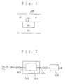
- Fig. 1 where, in order to make an electrical contact with source or drain n+ regions 82 of an MOS LSI formed on a p type Si substrate, contact holes 85 are formed in an insulating film 81 such as SIO2, and then tungsten (W) electrodes are attached to the surface of n+ regions 82 located inside contact holes 85.
- insulating film 81 such as SIO2
- W electrodes As a method for manufacturing the W electrodes, the method that by introducing WF6 and H2 gases into a reaction chamber, W electrodes are formed on surface 84 of n+ region 82 according to the following equation: WF6 + 3H2 ⁇ W + 6HF ... (1), has been examined.
- the reaction shown as (1) is thought to proceed in such a manner that deposited tungsten works as a catalyst, and the WF6 is reduced by H2 as it is adsorbed by the W. Therefore, this reaction is thought to proceed swiftly only in the case in which W has been deposited thicker than some particular thickness and the surface of the metal is kept pure. If the surface of W is not pure, the substrate must be heated to a temperature higher than 600°C in order for the reaction (1) to proceed. However, when the temperature of the substrate is increased, not only is the quality of the deposited W film reduced because the size of the crystal grain becomes large, but the chance of the formation of an undesired film is also increased as a result of a reaction between tungsten and impurities.
- the initial deposition of the W is thought to occur selectively only on the semiconductor surface according to the following reduction reaction 2WF6 + 3Si ⁇ 2W + 3SiF4 .... (2) after WF6 is adsorbed by Si surface 84 of n+ region 82. Therefore, if some other compounds are formed on the surface of n+ region and thus the pure semiconductor surface is not preserved, the reaction (2) will not proceed swiftly and, in other words, the selective deposition will not occur.
- the site where H2O or O2 is adsorbed serves as a source of nucleation in a deposition process, and the W film results even on the insulating film. Namely, the selectivity of deposition between n+ region 82 and insulating film 81 will be lowered.
- WF6 gas of low grade which gas, for example, usually includes more than 10 ppm of moisture
- WF6 reacts with H2O, generating HF which is extremely reactive, and HF thus generated corrodes not only metal but also polyimides and CTFE which are used for, for example, the seat of a valve and the conductance controller of a regulator.
- the purity of the source gas is decreased still more.
- the W films manufactured by using the prior art technologies are of poor quality, and the specific contact resistivity value of the film is as high as 10 ⁇ 4 to 10 ⁇ 5 ohm/cm2.
- the W film deposits on the insulating film as well as on the surface of Si.
- another aim to form the W film only on the Si surface located inside the contact holes has not been attained.
- the first aim of this invention is to provide a tungsten film forming apparatus comprising a reaction chamber, means for introducing WF6 into the reaction chamber, and means for introducing H2 into the reaction chamber, wherein at least that portion of the reaction chamber which is to be in contact with WF6 is made of metal materials whose surface is covered with a fluorinated passivation film consisting mainly of an almost stoichiometric metal fluoride .
- the second point of this invention is to provide a tungsten film forming apparatus according to the first aim, which includes a means for introducing F2 gas into the reaction chamber.
- the most striking characteristic of this invention is that the fluorinated passivation film mainly consisting of metal fluoride which is an almost stoichiometric amount, is formed at least on that portion of the interior wall of the reaction chamber which is to be in contact with WF6. It is obvious that this fluorinated passivation film can be formed on portions other than that which is to be in contact with WF6 inside the reaction chamber.
- This passivation film has been found by the present inventors to have extremely good corrosion-resistance to WF6 and to release little impurity gas.
- the material on which the fluorinated passivation film is formed is a metal or a metal alloy; for example, nickel, nickel alloy, aluminum, aluminum alloy, copper, copper alloy, stainless steel, cobalt, cobalt alloy, titan, titan alloy, and other metals and metal alloys. It is also possible that after forming a metal layer or a metal alloy layer by the use of appropriate layer forming means such as plating, evaporation, and sputtering, on the surface of appropriate materials including, for example, ceramics, the fluorinated passivation film is formed on the surface of the metal or the metal alloy layer. It should be noticed that for purpose of this disclosure all materials whose surfaces are covered with a metal or a metal alloy layer will hereinafter be referred to as metal materials.
- the metals and the metal alloys mentioned above aluminum and aluminum alloy are particularly suitable because they are inexpensive, and the passivation film which mainly consists of an almost stoichiometric metal fluoride is very corrosion-resistant as compared with the other metal and metal alloy materials.
- the passivation film which mainly consists of an almost stoichiometric metal fluoride is very corrosion-resistant as compared with the other metal and metal alloy materials.
- aluminum and aluminum alloy are readily oxidized and have an oxidized passivation film on their surface. The corrosion-resistance of the fluorinated passivation film formed on the oxidized passivation film is lower than that formed on the pure aluminum or aluminum alloy.
- the fluorinated passivation film without exposing the surface to atmosphere, i.e., maintaining the pure aluminum and aluminum alloy surface after the aluminum or aluminum alloy layer is formed in a high purity of atmosphere by a method such as sputtering.
- fluorinated passivation film The methods to form fluorinated passivation film are described in Japanese patent applications, "Metal materials with fluorinated passivation film and the apparatus using these metal materials," submitted on July 20, 1988 and “Metal materials with fluorinated passivation film and the apparatus using these materials,” submitted on January 13, 1989.
- the formation of the fluorinated passivation film for example, is carried out by following method.
- the natural oxidation film is removed from the surface of the metal material.
- the metal material is baked in a high purity atmosphere of inert gas so that the adsorbed impurities such as moisture will be desorbed from the metal surface. It is preferable that the impurity content of the inert gas is less than several ppb.
- the fluorinated passivation film is then formed on a portion of the surface or on the entire surface of the metal material, and is then annealed in ultra high purity atmosphere of inert gas whose impurity content is less than several ppb is preferable.
- the selected baking temperature is a matter of design choice provided that adsorbed moisture can be removed from the metal surface.
- a temperature 350 through 600°C is desirable and 400 through 600°C is preferable.
- the preferable baking time is 1 through 5 hours. At a temperature lower than 350°C, the adsorbed moisture cannot be removed completely from the metal surface. Therefore, if the metal is fluorinated under such condition, for example, in the case of Ni where the formed fluorinated passivation film may be composed of the NiF2.4H2O, a complete fluorinated passivation film which is a stoichiometric amount may not be obtained. In the case of aluminum and aluminum alloy, the baking temperature 150 through 400°C is desired, and the temperature 200 through 300°C is favorable.
- a temperature 200 through 500°C is desirable and a temperature 250 through 450°C is preferable for nickel, Monel, copper, copper alloy, and chromium.
- a fluorination time of 1 through 5 hours is preferable.
- the fluorinated passivation film which is thick enough and has excellent corrosion-resistance may not be obtained in some cases.
- the fluorination of metals is carried out at a temperature higher than 450°C, e.g., nickel, the crystal grain of nickel fluoride may be generated in the fluorinated passivation film, which may cause cracking and flaking off of the film.
- the fluorination temperature for Hastelloy C of 150 through 300°C is desirable and 150 through 250°C is preferable.
- an excellent corrosion-resistant passivation film may not be obtained because of flaking off of the film.
- the desirable temperature range for fluorination is 100 through 300°C although a preferable temperature range is 150 through 265°C.
- the time for fluorination is 1 through 5 hours.
- FeF2 is generated.
- FeF3 is generated at a temperature higher than 265°C. If a large amount of FeF3 is generated, the formed film may expand and result in cracking and flaking off of the film because the bulk density of FeF2 is 1.16 times that of FeF3.
- the desirable fluorination temperature range is 200 through 400°C, and preferable range is 250 through 350°C.
- the fluorination be carried out at atmospheric pressure. However, the fluorination can also be carried out under increased pressure which is less than about 2 atms in gauge pressure. It is preferable to carry out the fluorination in the atmosphere free from oxygen. Therefore, the preferable atmosphere consists of only fluorine or fluorine diluted by appropriate inert gas such as N2, Ar, He, and so forth.
- appropriate inert gas such as N2, Ar, He, and so forth.
- the atomic ratio of F to Ni was found to be 1.1 times as large as the stoichiometric ratio of NiF2.
- F exists in excess by a factor of 1.1 as compared to Ni.
- the excess F does not bond with Ni but exists without restriction in the passivation film.
- This film cannot be a corrosion-resistant material because the resistance to corrosion is inhibited by the excess F.
- All passivation films which have been reported up to now are the ones that include such excess F, and have not corrosion-resistance property at all.
- a temperature range of 300 through 600°C is desirable, and a range of 400 through 500°C is preferable for nickel, nickel alloy, copper, copper alloy, and chromium.
- a temperature range of 200 through 600°C is desirable and a range of 300 through 500°C is preferable.
- a range of 200 through 400°C is desirable, and a range of 250 through 400°C is preferable.
- the almost stoichiometric passivation film is obtained which is durable, dense, and highly adhesive to metal and has sufficient corrosion-resistance. It is a surprising phenomenon and has not been recognized up to now that the quality of the passivation film can be thus improved by the annealing treatment.
- the ratio of the metal atoms to the fluorine atoms in the fluorinated passivation film almost coincided with stoichiometric ratio of metal fluoride after the annealing treatment.
- the thickness of the fluorinated passivation film was measured with a Shimazu Seisakusho Model AEP-100 ellipsometer.
- the metal is fluorinated, it is preferable to remove the transmuted layer on the metal surface produced during surface machining and to make the surface smooth.
- R max represents the maximum height difference in peaks of surface.
- the fluorinated passivation film formed on the mirror finished surface whose R max is nearly 0.03-1.0 ⁇ m has been found to have excellent corrosion-resistance as compared with that formed on the surface without the mirror finish treatment.
- the method of the mirror finish treatment itself is a matter of design choice provided that the transmuted layer can be removed completely from the metal surface, and appropriate means can be chosen in various fields. As a typical example, composite electrolytic polishing is available.
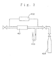
- FIG. 2 is a schematic representation of one example wherein interior surface of the reaction chamber is passivated.
- the reaction chamber 303 is passivated, moisture in the reaction chamber is purged at room temperature by introducing ultra high pure N2 or Ar into the reaction chamber through a gas supply line 301 at a flow rate of, e.g., about 10 1/min. Whether the moisture has been removed or not is confirmed, for example, by monitoring dew point of the purged gas with a dew point meter 305 installed at a purging line 304. After that, H2O molecules adsorbed by the interior surface of the reaction chamber are removed almost completely by heating the entire reaction chamber 303 to a baking temperature with an electric furnace 302.
- the fluorination of the interior surface of the reaction chamber is carried out by introducing a high purity gas of F2.
- ultra high pure N2 or Ar is again introduced into the chamber in order for the F2 gas remaining in the chamber to be purged. Even after purging is completed, ultra high pure N2 or Ar is allow to keep flowing and the fluorinated passivation film is annealed. The fluorinated passivation film thus formed is extremely stable to a corrosive gas.
- the W film forming apparatus can be fabricated by using the above-mentioned metal materials which have already been fluorinated. It is also possible to manufacture the apparatus by forming the fluorinated passivation film on a metal surface after the apparatus is assembled. The fluorination is carried out under the conditions mentioned above.
- the corrosion caused by WF6 and the release of the gas from the surface of the reaction chamber can be prevented. Namely, the WF6 gas and the surface of the substrate and the film can be prevented from being contaminated. As a result, a high quality W film can be deposited selectively only on the Si surface.
- the apparatus of the present invention has excellent corrosion-resistance not only to WF6 but also to HF, which is generated as a result of the following reaction: WF6 + 3H2 ⁇ W + 6HF Because HF has as a property that it removes a natural oxidation film, even if the SiO2 film is formed on the Si surface, the SiO2 films will be removed immediately. Therefore, the surface of Si is maintained clean at the initial stage of deposition.
- the portion of an H2 gas introducing means which is to be in contact with H2 gas is preferably constructed of material which will not release gas from its surface. It is preferable for such portion to be made of stainless steel whose surface is covered with the oxidized passivation film which will be discussed later, or metal materials whose surface is covered with the fluorinated passivation film, the same materials as those used for the reaction chamber.
- the stainless steel on which the thermal oxidation passivation film is formed is described in Japan patent application Sho 63-5389.
- One example is described as follows; the stainless steel having the oxidized passivation film which has a thickness of more than 50 ⁇ and is composed of two layers of Cr oxides and Fe oxides, and is prepared by heating and oxidizing stainless steel such as SUS 316L at a temperature from 400 to 500°C.
- the means for introducing WF6 and H2 gases into the reaction chamber are separately connected to the reaction chamber. It is also possible to connect these two means to a gas mixer and then to connect the gas mixer to the chamber through other appropriate means.
- the whole reaction chamber When self cleaning as described above is carried out, it is preferable to heat the whole reaction chamber uniformly with means installed for heating the whole reaction chamber because the W deposits adhering to the wall can be removed swiftly and uniformly.
- a heating means for example, the following device is available: the device in which the whole reaction chamber is surrounded by a water jacket, and mineral oil heated to a prescribed temperature is made to flow into the water jacket.
- the stainless steel with the oxidized passivation film can be used for the means introducing WF6 because this WF6 gas is not as corrosive as the WF6 gas containing moisture.
- the metal materials with the flourinated passivation film of the present invention can be used.
- the W film which has excellent properties for example, very low contact resistivity
- the portion in contact with F2 is, at least, made of stainless steel on which the oxidized passivation film is formed, or metal materials with the fluorinated passivation film.
- valves, regulators, and/or filters can be installed at appropriate positions, if necessary. Those portion of these devices which are to be in contact with gases are made up of the stainless steel whose surface was oxidized to form the oxidized passivation film, or metal materials with the fluorinated passivation film of this invention.
- Unreacted WF6 gas is, for example, treated and disposed of as follows.
- a copper or nickel column packed with pelletized NaCl is installed downstream of the reaction chamber and a washing column is installed downstream of the copper or nickel column, wherein waste gas is washed with a 10 % NaOH aqueous solution.
- WF6 is replaced with Cl2 according to the following reactions .
- the Cl2 gas reacts with the NaOH solution at the washing column, producing NaCl, and the removal of WF6 is completed. Even for this reason, it is also useful to attach the F2 introducing means to the reaction chamber.
- Fig. 1 is a schematic representation illustrating MOS IC on which the film is formed by using the apparatus of the present invention.
- Fig. 2 is a schematic representation illustrating an apparatus for forming the fluorinated passivation film on the wall of a reaction chamber.
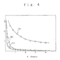
- Fig. 3 is a schematic representation showing an apparatus for evaluating the corrosion-resistance properties.
- Fig. 4 is a graph showing a gas releasing characteristic from the fluorinated passivation film.
- the thickness of the fluorinated passivation films formed at various temperatures is listed in Table 1. Cracking and flaking off were observed in the fluorinated passivation film formed at 305°C.
- Fig. 3 is a schematic representation illustrating an apparatus used for the evaluation of the passivation films.
- 401 is a SUS 316L 1/4 inches electrolytically polished tube
- 402 is a heating means (DC heating)
- 403 is a mercury manometer
- 404 is a gas cylinder. The results are summarized in Table 2.
- the metal materials subjected to the annealing treatment reacted little with WF6 as compared with those metal materials which had not been annealing treatment.
- the metal materials with the almost stoichiometric fluorinated passivation film of 660 ⁇ or more in thickness did not react with WF6 at all.
- the sample tube used for experiment was a SUS 316L tube of 1/4 inches diameter and 1 m length.
- the sample tubes had been left for 72 hours in a clean room where the temperature and humidity is kept at 25°C and 50%, respectively before the experiment was carried out.
- the evaluation was made by measuring the moisture content in the N2 gas after having passed through the tube by use of a dew point meter.
- a high purity N2 its moisture content being less than 0.1 ppm in volume, was flowed inside the tube at a rate of 500 cc/min.
- Fig 4 shows the results of the experiment carried out at room temperature.
- Fig .4 shows the results for the tube which was electrolytically polished (B), the tube which was, furthermore, fluorinated by F2 gas at 200°C for 2 hours(A), and the tube which was annealed in inert gas at 300°C for 2 hours after fluorination(C).
- a reaction chamber was fabricated by using the metal materials on which the fluorinated passivation film of 660 ⁇ in thickness, composed of an almost stoichiometric metal fluoride, was formed.
- This reaction chamber was separately connected to the means for introducing WF6, H2, and F2 gases.
- the means for introducing gas are the gas introducing tubes wherein a thermally oxidized passivation film is formed on the surface of stainless steel tube having a surface flatness equal to or less than 0.5 ⁇ m.
- the valves, regulators, and filters were attached to appropriate positions of the gas introducing tubes.
- valves, regulators, and filters which are to be in contact with introduced gases were constructed of stainless steel, whose surface has a flatness R max equal to or less than 0.5 ⁇ m and the thermal oxidation passivation film was formed on in a similar manner as for the gas introducing tubes.
- the deposition of the W film was carried out on the Si substrate according to the following procedure.
- the Silicon substrate was placed in the reaction chamber. Then, the reaction chamber and the piping system were purged by ultra high purity N2 gas at a flow rate of 10 1/min.
- the Si substrate used was the one that had the same structure as that shown in Fig. 1 and in which the diameter of contact hole was 0.5 ⁇ m.
- WF6, H2, and F2 gases were introduced separately to the chamber, and then the film formation of W was begun.
- the film forming condition was as follows: The gases of WF6 and H2 used were free from moisture.
- a self cleaning of the reaction chamber was carried out by stopping supply of the WF6 and H2 gases, and by introducing only F2 gas.
- the thickness of the films formed at various fluorination temperatures is shown in Table 4. The crystal grain boundary, cracking, or flaking off has not been observed in the passivation films formed at various fluorination temperatures on Ni films which had been formed by a sputtering method on an SUS 316L plate and a quartz plate.
- the passivation film thus obtained was found to have a composition of NiF2 . 0, indicating that nickel fluoride was an almost stoichiometric amount.
- the corrosion-resistance characteristic to WF6 was evaluated in the similar way as in the embodiment 1. The result is listed in Table 5.
- the amount of the reacted WF6 is a little for the metal materials with annealing treatment, showing excellent corrosion-resistance.
- the amount of reaction was not observed and excellent corrosion-resistance was recognized.
- the metal material with the film of 200 ⁇ or more in thickness was also had excellent corrosion-resistant to the HF gas.
- the film forming apparatus was fabricated by using the metal materials with the annealed passivation film of 200 ⁇ in thickness, and then the film formation of W was made with this apparatus.
- the W film was formed only on the Si surface located inside of the contact holes, and the contact resistivity was 10 ⁇ 8 - 10 ⁇ 9 ohm/cm2.
- Hastelloy C Ni51 - Mo19 - Cr17 - Fe6 - W5 in wt% ) which had a surface flatness R max of 0.03 - 1.0 ⁇ m was fluorinated in 100 % F2 gas for 1 - 5 hours and then annealed at 400°C in inert gas for 2 hours, after having been baked at 500°C in ultra high purity atmosphere of N2 gas for one hour.
- the thickness of the films formed at various fluorination temperatures is listed in Table 6. Neither cracking nor flaking off was observed in the films which were fluorinated at 200 and 250°C.
- the corrosion-resistance characteristic to WF6 and HF gases was evaluated.
- the metal material which had a film of 200 ⁇ or more in thickness and was annealed after film formation showed excellent corrosion-resistance to WF6 and HF gases as well as in the cases of the embodiments 1 and 2.
- the W film forming apparatus was fabricated by using the metal material which had a fluorinated film of 200 ⁇ in thickness and was annealed, and then the W film was formed with this apparatus in a similar manner as shown in the embodiment 1.
- the W film was formed only on the Si surface located inside the contact holes and the contact resistivity was in the range from 10 ⁇ 8 - 10 ⁇ 9 ohm/cm2. Also, the self cleaning of the reaction chamber was carried out satisfactorily as well as in the embodiment 1.
- a polished plate of Monel ( Ni66 - Cu29 - A13 ) which had a surface flatness R max of 0.03 - 1.0 ⁇ m was fluorinated in 100 % F2 for 1 - 5 hours after having been baked at 500°C in ultra high purity atmosphere of N2 for one hour.
- the thickness of the films and the film forming temperature are listed in Table 7. Although a slight nonuniformity in film color was observed for the metal material which was fluorinated at 500°C, Neither cracking nor flaking off was observed.
- the W film forming apparatus was fabricated by using the metal material which had a fluorinated film of 200 ⁇ in thickness and was annealed, and then the W film was formed with this apparatus in a similar manner as in the embodiment 1.
- the W film was formed only on the Si surface located inside the contact holes and the contact resistivity was in the range from 10 ⁇ 8 - 10 ⁇ 9 ohm/cm2. Also, the self cleaning of the reaction chamber was carried out satisfactorily as well as in the embodiment 1.
- a polished copper plate which had a surface flatness R max of 0.03 - 1.0 ⁇ m and a SUS-316L substrate on which a copper film of 4000 ⁇ in thickness was formed by a method of sputtering were fluorinated in 100 % F2 for 1 - 5 hours and then annealed at 500°C in inert gas for 2 hours, after having been baked at 500°C in ultra high purity atmosphere of N2 for one hour.
- the thickness of the films formed at various temperatures are listed in Table 8.
- the W film forming apparatus was fabricated by using the metal material which had a fluorinated film of 200 ⁇ in thickness and was annealed, and then the W film was formed with this apparatus in a similar manner as shown in the embodiment 1.
- the W film was formed only on the Si surface located inside the contact holes and the contact resistivity was in the range from 10 ⁇ 8 - 10 ⁇ 9 ohm/cm2. Also, the self cleaning of the reaction chamber was carried out satisfactorily as well as in the embodiment 1.
- a Cr film of 4000 ⁇ in thickness was formed on a SUS 316L substrate by a method of sputtering. Then, the surface of Cr film was fluorinated in 100 % F2 for 1 - 5 hours after having been baked in ultra high purity atmosphere of N2 gas at 500°C for one hour. Thereafter these substrates were annealed in inert gas at 500°C for 2 hours.
- the thickness of the films formed at various fluorination temperatures is shown in Table 9. Neither Cracking nor flaking was observed in any passivation film formed at various temperatures.
- the W film forming apparatus was fabricated by using the metal material which had a fluorinated film of 200 ⁇ in thickness and was annealed, and then the W film was formed with this apparatus in a similar manner as shown in the embodiment 1.
- the W film was formed only on the Si surface located inside the contact holes and the contact resistivity was in the range from 10 ⁇ 8 - 10 ⁇ 9 ohm/cm2. Also, the self cleaning of the reaction chamber was carried out satisfactorily as well as in the embodiment 1.
- Polished plates of aluminum and aluminum alloy which had a surface flatness R max of 0.03 - 1.0 ⁇ m and an aluminum film of 2000 ⁇ in thickness formed on a SUS-316L substrate by a method of sputtering were fluorinated in 100 % F2 for 1 - 5 hours and then annealed at 350°C in inert gas for 2 hours, after having been baked at 300°C in ultra high purity atmosphere of N2 for one hour.
- the thickness of the films formed at various fluorination temperature are listed in Table 10.
- the W film forming apparatus was fabricated by using the metal materials plate which had a fluorinated film of 200 ⁇ in thickness and was annealed, and then the W film was formed with this apparatus in a similar manner as shown in the embodiment 1.
- the W film was formed only on the Si surface located inside the contact holes and the contact resistivity was in the range from 10 ⁇ 8 - 10 ⁇ 9 ohm/cm2. Also, the self cleaning of the reaction chamber was carried out satisfactorily as well as in the embodiment 1.
- a polished plate of Brass ( Cu70 - Zn30 ) which had a surface flatness R max 0.03 - 1.0 ⁇ m was fluorinated in 100 % F2 gas for 1 - 5 hours and then annealed at 350°C in inert gas for 2 hours, after being baked at 300°C in ultra high purity atmosphere of N2 gas for one hour.
- the thickness of the films formed at various temperatures is listed in Table 11. Neither cracking nor flaking was observed in the films fluorinated at both temperatures.
- the W film forming apparatus was fabricated by using the metal material which had a fluorinated film of 200 ⁇ in thickness and was annealed, and then the W film was formed with this apparatus in a similar manner as shown in the embodiment 1.
- the W film was formed only on the Si surface located inside the contact holes and the contact resistivity was in the range from 10 ⁇ 8 - 10 ⁇ 9 ohm/cm2. Also, the self cleaning of the reaction chamber was carried out satisfactorily as well as in the embodiment 1.
- the portions of a WF6 gas introducing tube, a F2 gas introducing tube, valves, regulators, and filters, which were to be in contact with WF6 or HF gases were made of the metal material, the surface of which was the fluorinated passivation film of 660 ⁇ in thickness.
- the other constitutions of the apparatus were the same as those shown in the embodiment 1.
- the W film was formed with this apparatus in the same way as shown in the embodiment 1, which led the result that remarkably excellent characteristic such as the contact resistivity of 10 ⁇ 9 ohm/cm2, could be reliably obtained.
- the present invention it becomes possible to deposit at a low temperature a high quality tungsten film whose contact resistivity is very low on the silicone substrate.
- a high quality tungsten film whose contact resistivity is very low on the silicone substrate.
- the W film only on the Si surface located inside the contact holes with high selectivity.
Landscapes
- Chemical & Material Sciences (AREA)
- General Chemical & Material Sciences (AREA)
- Chemical Kinetics & Catalysis (AREA)
- Engineering & Computer Science (AREA)
- Materials Engineering (AREA)
- Mechanical Engineering (AREA)
- Metallurgy (AREA)
- Organic Chemistry (AREA)
- Chemical Vapour Deposition (AREA)
- Internal Circuitry In Semiconductor Integrated Circuit Devices (AREA)
- Electrodes Of Semiconductors (AREA)
Applications Claiming Priority (3)
| Application Number | Priority Date | Filing Date | Title |
|---|---|---|---|
| JP1090226A JP2730695B2 (ja) | 1989-04-10 | 1989-04-10 | タングステン膜の成膜装置 |
| JP90226/89 | 1989-04-10 | ||
| PCT/JP1990/000456 WO1990012418A1 (fr) | 1989-04-10 | 1990-04-04 | Dispositif de formation d'un film de tungstene |
Publications (3)
| Publication Number | Publication Date |
|---|---|
| EP0428733A1 true EP0428733A1 (de) | 1991-05-29 |
| EP0428733A4 EP0428733A4 (en) | 1993-03-03 |
| EP0428733B1 EP0428733B1 (de) | 1997-07-09 |
Family
ID=13992569
Family Applications (1)
| Application Number | Title | Priority Date | Filing Date |
|---|---|---|---|
| EP90905657A Expired - Lifetime EP0428733B1 (de) | 1989-04-10 | 1990-04-04 | Vorrichtung zur Herstellung eines Wolframfilmes |
Country Status (6)
| Country | Link |
|---|---|
| US (1) | US5149378A (de) |
| EP (1) | EP0428733B1 (de) |
| JP (1) | JP2730695B2 (de) |
| KR (1) | KR0144695B1 (de) |
| DE (1) | DE69031024T2 (de) |
| WO (1) | WO1990012418A1 (de) |
Cited By (5)
| Publication number | Priority date | Publication date | Assignee | Title |
|---|---|---|---|---|
| EP0648860A1 (de) * | 1993-10-14 | 1995-04-19 | Applied Materials, Inc. | Verfahren zur Vorbehandlung von Aluminiumoberflächen einer Aufdampfungskammer vor der Auftragung einer Wolframsilizid-Schicht auf ein Substrat in der Kammer |
| US5482749A (en) * | 1993-06-28 | 1996-01-09 | Applied Materials, Inc. | Pretreatment process for treating aluminum-bearing surfaces of deposition chamber prior to deposition of tungsten silicide coating on substrate therein |
| US5510297A (en) * | 1993-06-28 | 1996-04-23 | Applied Materials, Inc. | Process for uniform deposition of tungsten silicide on semiconductor wafers by treatment of susceptor having aluminum nitride surface thereon with tungsten silicide after cleaning of susceptor |
| US6090706A (en) * | 1993-06-28 | 2000-07-18 | Applied Materials, Inc. | Preconditioning process for treating deposition chamber prior to deposition of tungsten silicide coating on active substrates therein |
| EP0760526A4 (de) * | 1994-05-17 | 2001-01-10 | Hitachi Ltd | Einrichtung und verfahren zur plasma-behandlung |
Families Citing this family (37)
| Publication number | Priority date | Publication date | Assignee | Title |
|---|---|---|---|---|
| KR100198678B1 (ko) | 1996-02-28 | 1999-06-15 | 구본준 | 금속 배선 구조 및 형성방법 |
| JP4125406B2 (ja) | 1997-08-08 | 2008-07-30 | 忠弘 大見 | フッ化不働態処理が施された溶接部材の溶接方法および再フッ化不働態処理方法ならびに溶接部品 |
| US6440852B1 (en) * | 1999-01-26 | 2002-08-27 | Agere Systems Guardian Corp. | Integrated circuit including passivated copper interconnection lines and associated manufacturing methods |
| US6368410B1 (en) * | 1999-06-28 | 2002-04-09 | General Electric Company | Semiconductor processing article |
| US6391146B1 (en) * | 2000-04-11 | 2002-05-21 | Applied Materials, Inc. | Erosion resistant gas energizer |
| US6673323B1 (en) | 2000-03-24 | 2004-01-06 | Applied Materials, Inc. | Treatment of hazardous gases in effluent |
| JP4763245B2 (ja) * | 2004-03-17 | 2011-08-31 | 財団法人国際科学振興財団 | 表示装置等電子装置の製造装置、製造方法および表示装置等の電子装置 |
| KR101338301B1 (ko) * | 2005-09-16 | 2013-12-09 | 고에키자이단호진 고쿠사이카가쿠 신고우자이단 | 표시 장치 등의 전자 장치의 제조 장치, 제조 방법, 및표시 장치 등의 전자 장치 |
| US8021492B2 (en) | 2007-05-29 | 2011-09-20 | United Microelectronics Corp. | Method of cleaning turbo pump and chamber/turbo pump clean process |
| JP4680246B2 (ja) * | 2007-10-03 | 2011-05-11 | キヤノンアネルバ株式会社 | 気相成長装置の異常生成物除去方法 |
| FR2956123B1 (fr) * | 2010-02-08 | 2017-10-27 | Dalic | Procede de protection d'un substrat metallique contre la corrosion et l'abrasion, et substrat metallique obtenu par ce procede. |
| JP5335843B2 (ja) * | 2011-03-22 | 2013-11-06 | 公益財団法人国際科学振興財団 | 電子装置用基板の製造法 |
| US10224224B2 (en) | 2017-03-10 | 2019-03-05 | Micromaterials, LLC | High pressure wafer processing systems and related methods |
| US10622214B2 (en) | 2017-05-25 | 2020-04-14 | Applied Materials, Inc. | Tungsten defluorination by high pressure treatment |
| KR102574914B1 (ko) | 2017-06-02 | 2023-09-04 | 어플라이드 머티어리얼스, 인코포레이티드 | 보론 카바이드 하드마스크의 건식 스트리핑 |
| US10269571B2 (en) | 2017-07-12 | 2019-04-23 | Applied Materials, Inc. | Methods for fabricating nanowire for semiconductor applications |
| US10179941B1 (en) | 2017-07-14 | 2019-01-15 | Applied Materials, Inc. | Gas delivery system for high pressure processing chamber |
| JP6947914B2 (ja) | 2017-08-18 | 2021-10-13 | アプライド マテリアルズ インコーポレイテッドApplied Materials,Incorporated | 高圧高温下のアニールチャンバ |
| US10276411B2 (en) | 2017-08-18 | 2019-04-30 | Applied Materials, Inc. | High pressure and high temperature anneal chamber |
| CN111095524B (zh) | 2017-09-12 | 2023-10-03 | 应用材料公司 | 用于使用保护阻挡物层制造半导体结构的设备和方法 |
| US10643867B2 (en) | 2017-11-03 | 2020-05-05 | Applied Materials, Inc. | Annealing system and method |
| KR102585074B1 (ko) | 2017-11-11 | 2023-10-04 | 마이크로머티어리얼즈 엘엘씨 | 고압 프로세싱 챔버를 위한 가스 전달 시스템 |
| SG11202003438QA (en) | 2017-11-16 | 2020-05-28 | Applied Materials Inc | High pressure steam anneal processing apparatus |
| JP2021503714A (ja) | 2017-11-17 | 2021-02-12 | アプライド マテリアルズ インコーポレイテッドApplied Materials,Incorporated | 高圧処理システムのためのコンデンサシステム |
| JP7299898B2 (ja) | 2018-01-24 | 2023-06-28 | アプライド マテリアルズ インコーポレイテッド | 高圧アニールを用いたシーム修復 |
| CN111902929B (zh) | 2018-03-09 | 2025-09-19 | 应用材料公司 | 用于含金属材料的高压退火处理 |
| US10714331B2 (en) | 2018-04-04 | 2020-07-14 | Applied Materials, Inc. | Method to fabricate thermally stable low K-FinFET spacer |
| US10950429B2 (en) | 2018-05-08 | 2021-03-16 | Applied Materials, Inc. | Methods of forming amorphous carbon hard mask layers and hard mask layers formed therefrom |
| US10566188B2 (en) | 2018-05-17 | 2020-02-18 | Applied Materials, Inc. | Method to improve film stability |
| US10704141B2 (en) | 2018-06-01 | 2020-07-07 | Applied Materials, Inc. | In-situ CVD and ALD coating of chamber to control metal contamination |
| US10748783B2 (en) | 2018-07-25 | 2020-08-18 | Applied Materials, Inc. | Gas delivery module |
| US10675581B2 (en) | 2018-08-06 | 2020-06-09 | Applied Materials, Inc. | Gas abatement apparatus |
| JP7179172B6 (ja) | 2018-10-30 | 2022-12-16 | アプライド マテリアルズ インコーポレイテッド | 半導体用途の構造体をエッチングするための方法 |
| KR20210077779A (ko) | 2018-11-16 | 2021-06-25 | 어플라이드 머티어리얼스, 인코포레이티드 | 강화된 확산 프로세스를 사용한 막 증착 |
| WO2020117462A1 (en) | 2018-12-07 | 2020-06-11 | Applied Materials, Inc. | Semiconductor processing system |
| US20200203127A1 (en) | 2018-12-20 | 2020-06-25 | L'Air Liquide, Société Anonyme pour I'Etude et I'Exploitation des Procédés Georges Claude | Systems and methods for storage and supply of f3no-free fno gases and f3no-free fno gas mixtures for semiconductor processes |
| US11901222B2 (en) | 2020-02-17 | 2024-02-13 | Applied Materials, Inc. | Multi-step process for flowable gap-fill film |
Family Cites Families (5)
| Publication number | Priority date | Publication date | Assignee | Title |
|---|---|---|---|---|
| FR1405264A (fr) * | 1964-05-12 | 1965-07-09 | Commissariat Energie Atomique | Procédé de fabrication d'enceintes sous vide |
| US3591426A (en) * | 1968-10-30 | 1971-07-06 | Nasa | Corrosion resistant beryllium |
| JPS62230981A (ja) * | 1986-03-31 | 1987-10-09 | Toshiba Corp | 薄膜形成方法 |
| JPH0672304B2 (ja) * | 1987-02-20 | 1994-09-14 | マツダ株式会社 | タングステンカ−バイト層を析出させる処理装置 |
| US5009963A (en) * | 1988-07-20 | 1991-04-23 | Tadahiro Ohmi | Metal material with film passivated by fluorination and apparatus composed of the metal material |
-
1989
- 1989-04-10 JP JP1090226A patent/JP2730695B2/ja not_active Expired - Fee Related
-
1990
- 1990-04-04 WO PCT/JP1990/000456 patent/WO1990012418A1/ja not_active Ceased
- 1990-04-04 EP EP90905657A patent/EP0428733B1/de not_active Expired - Lifetime
- 1990-04-04 US US07/613,730 patent/US5149378A/en not_active Expired - Lifetime
- 1990-04-04 DE DE69031024T patent/DE69031024T2/de not_active Expired - Lifetime
- 1990-12-10 KR KR90702595A patent/KR0144695B1/ko not_active Expired - Fee Related
Cited By (5)
| Publication number | Priority date | Publication date | Assignee | Title |
|---|---|---|---|---|
| US5482749A (en) * | 1993-06-28 | 1996-01-09 | Applied Materials, Inc. | Pretreatment process for treating aluminum-bearing surfaces of deposition chamber prior to deposition of tungsten silicide coating on substrate therein |
| US5510297A (en) * | 1993-06-28 | 1996-04-23 | Applied Materials, Inc. | Process for uniform deposition of tungsten silicide on semiconductor wafers by treatment of susceptor having aluminum nitride surface thereon with tungsten silicide after cleaning of susceptor |
| US6090706A (en) * | 1993-06-28 | 2000-07-18 | Applied Materials, Inc. | Preconditioning process for treating deposition chamber prior to deposition of tungsten silicide coating on active substrates therein |
| EP0648860A1 (de) * | 1993-10-14 | 1995-04-19 | Applied Materials, Inc. | Verfahren zur Vorbehandlung von Aluminiumoberflächen einer Aufdampfungskammer vor der Auftragung einer Wolframsilizid-Schicht auf ein Substrat in der Kammer |
| EP0760526A4 (de) * | 1994-05-17 | 2001-01-10 | Hitachi Ltd | Einrichtung und verfahren zur plasma-behandlung |
Also Published As
| Publication number | Publication date |
|---|---|
| DE69031024T2 (de) | 1997-10-30 |
| EP0428733A4 (en) | 1993-03-03 |
| JP2730695B2 (ja) | 1998-03-25 |
| KR920700469A (ko) | 1992-02-19 |
| EP0428733B1 (de) | 1997-07-09 |
| DE69031024D1 (de) | 1997-08-14 |
| US5149378A (en) | 1992-09-22 |
| JPH02270964A (ja) | 1990-11-06 |
| WO1990012418A1 (fr) | 1990-10-18 |
| KR0144695B1 (en) | 1998-08-17 |
Similar Documents
| Publication | Publication Date | Title |
|---|---|---|
| US5149378A (en) | Tungsten film forming apparatus | |
| US5009963A (en) | Metal material with film passivated by fluorination and apparatus composed of the metal material | |
| US5259935A (en) | Stainless steel surface passivation treatment | |
| US20040134427A1 (en) | Deposition chamber surface enhancement and resulting deposition chambers | |
| EP0352061A2 (de) | Metallischer Werkstoff mit durch Fluorierung passiviertem Film und aus dem metallischen Werkstoff bestehende Anlage | |
| EP0512782B1 (de) | Verfahren zur Herstellung einer Oxidschicht auf der Oberfläche von rostfreiem Stahl | |
| EP0596121A1 (de) | Verfahren zur herstellung einer passivschicht auf stahl und der verbindungsstelle von rostfreiem stahl und flüssigkeit und ga | |
| JP2000299289A (ja) | クリーニングガス及び真空処理装置のクリーニング方法 | |
| EP1007763A1 (de) | Verfahren zum reduzieren von metallkontaminationen während der halbleiterherstellung in einem reaktor, der metallteile enthält | |
| US6231690B1 (en) | Method of oxidizing inner surface of ferritic stainless pipe | |
| US5789086A (en) | Stainless steel surface having passivation film | |
| JPH0285358A (ja) | 減圧装置 | |
| US5224998A (en) | Apparatus for oxidation treatment of metal | |
| Sanjurjo et al. | Titanium-based coatings on copper by chemical vapor deposition in fluidized bed reactors | |
| JPH02263972A (ja) | フッ化不動態膜が形成された金属材料、その金属材料を用いたガス装置、並びに該フッ化不動態膜の形成方法 | |
| JP2976333B2 (ja) | ステンレス鋼及びその製造方法並びに減圧装置 | |
| JPH0641629A (ja) | 酸化クロムを主成分とする酸化不動態膜の形成方法及びステンレス鋼 | |
| WO1995018240A1 (en) | Austenitic stainless steel, piping system and fluid-contacting parts | |
| JP2720716B2 (ja) | 耐食性に優れる高純度ガス用オーステナイト系ステンレス鋼材及びその製造方法 | |
| JPH03215656A (ja) | フッ化不働態膜が形成されたステンレス鋼、その製造方法並びにそのステンレスを用いた装置 | |
| KR950012809B1 (ko) | 불화부동태막이 형성된 금속재료 및 그 금속재료를 사용한 장치 | |
| WO1990007587A1 (fr) | Dispositif d'alimentation en gaz de traitement | |
| JP3037928B2 (ja) | ステンレス鋼及びその製造方法並びに減圧装置 | |
| JPH04333570A (ja) | Hfガスによる窒化珪素のクリーニング方法 | |
| JP2737551B2 (ja) | 耐食性に優れる高純度ガス用オーステナイト系ステンレス鋼材の製造方法 |
Legal Events
| Date | Code | Title | Description |
|---|---|---|---|
| PUAI | Public reference made under article 153(3) epc to a published international application that has entered the european phase |
Free format text: ORIGINAL CODE: 0009012 |
|
| AK | Designated contracting states |
Kind code of ref document: A1 Designated state(s): BE CH DE FR GB IT LI NL |
|
| 17P | Request for examination filed |
Effective date: 19910408 |
|
| RAP1 | Party data changed (applicant data changed or rights of an application transferred) |
Owner name: OHMI, TADAHIRO Owner name: HASHIMOTO KASEI KABUSHIKI-KAISYA |
|
| A4 | Supplementary search report drawn up and despatched |
Effective date: 19930109 |
|
| AK | Designated contracting states |
Kind code of ref document: A4 Designated state(s): BE CH DE FR GB IT LI NL |
|
| 17Q | First examination report despatched |
Effective date: 19950410 |
|
| GRAG | Despatch of communication of intention to grant |
Free format text: ORIGINAL CODE: EPIDOS AGRA |
|
| GRAH | Despatch of communication of intention to grant a patent |
Free format text: ORIGINAL CODE: EPIDOS IGRA |
|
| GRAH | Despatch of communication of intention to grant a patent |
Free format text: ORIGINAL CODE: EPIDOS IGRA |
|
| GRAA | (expected) grant |
Free format text: ORIGINAL CODE: 0009210 |
|
| AK | Designated contracting states |
Kind code of ref document: B1 Designated state(s): BE CH DE FR GB IT LI NL |
|
| PG25 | Lapsed in a contracting state [announced via postgrant information from national office to epo] |
Ref country code: NL Free format text: LAPSE BECAUSE OF FAILURE TO SUBMIT A TRANSLATION OF THE DESCRIPTION OR TO PAY THE FEE WITHIN THE PRESCRIBED TIME-LIMIT Effective date: 19970709 Ref country code: IT Free format text: LAPSE BECAUSE OF FAILURE TO SUBMIT A TRANSLATION OF THE DESCRIPTION OR TO PAY THE FEE WITHIN THE PRE;WARNING: LAPSES OF ITALIAN PATENTS WITH EFFECTIVE DATE BEFORE 2007 MAY HAVE OCCURRED AT ANY TIME BEFORE 2007. THE CORRECT EFFECTIVE DATE MAY BE DIFFERENT FROM THE ONE RECORDED.SCRIBED TIME-LIMIT Effective date: 19970709 Ref country code: CH Free format text: LAPSE BECAUSE OF FAILURE TO SUBMIT A TRANSLATION OF THE DESCRIPTION OR TO PAY THE FEE WITHIN THE PRESCRIBED TIME-LIMIT Effective date: 19970709 Ref country code: LI Free format text: LAPSE BECAUSE OF FAILURE TO SUBMIT A TRANSLATION OF THE DESCRIPTION OR TO PAY THE FEE WITHIN THE PRESCRIBED TIME-LIMIT Effective date: 19970709 Ref country code: BE Effective date: 19970709 |
|
| REG | Reference to a national code |
Ref country code: CH Ref legal event code: EP |
|
| ET | Fr: translation filed | ||
| REF | Corresponds to: |
Ref document number: 69031024 Country of ref document: DE Date of ref document: 19970814 |
|
| NLV1 | Nl: lapsed or annulled due to failure to fulfill the requirements of art. 29p and 29m of the patents act | ||
| REG | Reference to a national code |
Ref country code: CH Ref legal event code: PL |
|
| PLBE | No opposition filed within time limit |
Free format text: ORIGINAL CODE: 0009261 |
|
| STAA | Information on the status of an ep patent application or granted ep patent |
Free format text: STATUS: NO OPPOSITION FILED WITHIN TIME LIMIT |
|
| 26N | No opposition filed | ||
| REG | Reference to a national code |
Ref country code: GB Ref legal event code: IF02 |
|
| PGFP | Annual fee paid to national office [announced via postgrant information from national office to epo] |
Ref country code: DE Payment date: 20090528 Year of fee payment: 20 Ref country code: FR Payment date: 20090421 Year of fee payment: 20 |
|
| PGFP | Annual fee paid to national office [announced via postgrant information from national office to epo] |
Ref country code: GB Payment date: 20090424 Year of fee payment: 20 |
|
| REG | Reference to a national code |
Ref country code: GB Ref legal event code: PE20 Expiry date: 20100403 |
|
| PG25 | Lapsed in a contracting state [announced via postgrant information from national office to epo] |
Ref country code: GB Free format text: LAPSE BECAUSE OF EXPIRATION OF PROTECTION Effective date: 20100403 |
|
| PG25 | Lapsed in a contracting state [announced via postgrant information from national office to epo] |
Ref country code: DE Free format text: LAPSE BECAUSE OF EXPIRATION OF PROTECTION Effective date: 20100404 |