EP0429055A2 - Datenformat für Informationspakete - Google Patents
Datenformat für Informationspakete Download PDFInfo
- Publication number
- EP0429055A2 EP0429055A2 EP90122166A EP90122166A EP0429055A2 EP 0429055 A2 EP0429055 A2 EP 0429055A2 EP 90122166 A EP90122166 A EP 90122166A EP 90122166 A EP90122166 A EP 90122166A EP 0429055 A2 EP0429055 A2 EP 0429055A2
- Authority
- EP
- European Patent Office
- Prior art keywords
- information
- bit
- control
- received
- bit information
- Prior art date
- Legal status (The legal status is an assumption and is not a legal conclusion. Google has not performed a legal analysis and makes no representation as to the accuracy of the status listed.)
- Granted
Links
Images


Classifications
-
- H—ELECTRICITY
- H04—ELECTRIC COMMUNICATION TECHNIQUE
- H04L—TRANSMISSION OF DIGITAL INFORMATION, e.g. TELEGRAPHIC COMMUNICATION
- H04L49/00—Packet switching elements
- H04L49/90—Buffering arrangements
- H04L49/9057—Arrangements for supporting packet reassembly or resequencing
-
- H—ELECTRICITY
- H04—ELECTRIC COMMUNICATION TECHNIQUE
- H04L—TRANSMISSION OF DIGITAL INFORMATION, e.g. TELEGRAPHIC COMMUNICATION
- H04L49/00—Packet switching elements
- H04L49/90—Buffering arrangements
-
- H—ELECTRICITY
- H04—ELECTRIC COMMUNICATION TECHNIQUE
- H04L—TRANSMISSION OF DIGITAL INFORMATION, e.g. TELEGRAPHIC COMMUNICATION
- H04L49/00—Packet switching elements
- H04L49/90—Buffering arrangements
- H04L49/9042—Separate storage for different parts of the packet, e.g. header and payload
-
- H—ELECTRICITY
- H04—ELECTRIC COMMUNICATION TECHNIQUE
- H04L—TRANSMISSION OF DIGITAL INFORMATION, e.g. TELEGRAPHIC COMMUNICATION
- H04L69/00—Network arrangements, protocols or services independent of the application payload and not provided for in the other groups of this subclass
- H04L69/22—Parsing or analysis of headers
Definitions
- This invention relates to a format for representing data and, more particularly, to a circuit for efficiently formatting a fixed number of serially received information units into a single block for transmission.
- information units Between separate computers or computer networks often requires a reformatting of the information contained in the information units.
- These information units generally contain a number of bits of either data information, control information or null information along with a bit or set of bits for identifying the type of information.
- the 9 bits ⁇ m:0> can be sent serially to a "server" interface for a second computer or computer network.
- the server is a part hardware and part software device designed to perform a specific function for a number of "clients" in a network.
- a client is the software operating a device such as a computer or an intelligent peripheral forming a part of the second network.
- the m-bit information units sent from the first network must be reformatted into n-bit information units for processing by the n-bit second network.
- the first network may require that only groups or "packets" of information units be forwarded over a serial line to the second network at one time.
- a known system processes packets of serially received m-bit information units by storing the information units and then expanding each m-bit information unit into a 16 bit word using a 16 bit latch, the output of which is fed to the n-bit network.
- the 16-bit information units can then be processed, one at a time, by a client in the byte oriented network.
- the client must individually determine for each 16-bit information unit whether the actual information in that information unit is user data, control information, or null data. This decreases the processing efficiency of the client as well as requiring more available memory space for expanding the m-bit information units into 2n-bit information units.
- the present invention overcomes these problems by forming a fixed length packet of serially received information units into a block which can then be transmitted to a client for subsequent processing.
- the bit or bits that indicate whether the information is control or data are collected for each information unit that is serially received in the packet from the m-bit network.
- the collection occurs at a device, e.g. a server, in which the information units are converted into the block.
- the indicator bit or bits are stored in a block header as a control/data bitmap.
- the remaining bits are stored in sequential locations in the block, each location corresponding with the location of its control/data bit or bits in the control/data bitmap.
- a fixed length block (corresponding to the number of information units in a packet) of information is therefore assembled in the server and stored in the server memory.
- the block can then be transmitted to the desired "client” in the n-bit network for processing, but preferably, the block is converted into a variable length block before being sent to the n-bit network as described in copending European patent application * , ) filed on even date herewith, the disclosure of which is hereby incorporated by reference. *) (Attorney file: DKK 63 EP); See Annex 1
- the server is shown as part of the n-bit network coupled directly to the m-bit network, it is understood that the server could: couple with the other network through another server; independently couple the two networks; or be a part of the m-bit network.
- the block therefore further includes a channel number field in its header.
- the channel number field stores the number of the channel (in the protocol of the m-bit network, the channel number is always the first information unit in the packet and is the only information unit not having a control/data indicator) on which the packet was received over the serial line.
- the header of the block further includes a valid information unit counter field which stores a count of the actual information received in the packet.
- a counter is incremented for each actual information unit received in the packet. Because the packets are of a fixed length, the m-bit network must sometimes fill the packet with null information units prior to delivering the packet over the serial line. By knowing the value of the counter field and the total number of information units in the block, the number of null information units can also be determined.
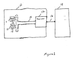
- a first computer or computer network 10 includes a bus 18, e.g., an Ethernet bus, coupling a plurality of devices 11, 13 to a server 12.
- the server 12 is further coupled over a high capacity serial line 16, e.g., optical fiber, hardwired line, etc., to a second computer or computing network 14.
- the network 14 supplies fixed length "packets" of information units from one network over the serial line 16 to communicate with the other network. While the discussion herein relates to only one communication over serial line 16, it is to be understood that information may be communicated over one of several channels on the serial line 16 in a multiplexed fashion thus requiring a channel number indicator in the packet.
- the devices 11, 13 operate on 8-bit boundaries of information, e.g., bytes, words or longwords.
- the server 12 In order for network 14 (hereinafter the "m-bit network”) to communicate with the network 10 (the “n-bit network”), the server 12 functions to provide an efficient data representation for a fixed length packet of m-bit information units received from m-bit network 14 over the serial line 16. This data representation (along with header information) is referred to as a "block" of information.
- the server 12 receives a packet of m-bit information units over serial line 16 from the m-bit network 14.
- the server's hardware Figure 3) then formats the m-bit information units into a block for efficient handling by the n-bit network 10.
- One example of a fixed length packet has seventeen information units, including a channel number information unit and sixteen m-bit control, data, or null information units. This fixed length packet is then forwarded over serial line 16 to the server 12. Each packet of information units is used to formulate one block.
- each successive m-bit information unit includes (m-1) bits of either control or data information.
- the m th bit is used to indicate whether the remaining (m-1) bits are either control or data. Only the logical channel number is a full m-bits wide. For example, if the m th bit is set equal to 1, then the information unit is a data information unit. Alternately, if the m th bit equals 0, then the information unit contains control information. Further, because each packet must contain seventeen information units, the network 14 will sometimes deliver null information units. Once a null information unit is sent, all remaining information units necessary to fill the packet must also be null units.
- FIG. 2 is a diagram illustrating an embodiment of the data representation formed by the server 12 in the present invention.
- the block 24 comprises five "longwords", i.e., a 32-bit word, including a 32-bit header 20.
- the header 20 includes three fields: logical channel number 25, bits ⁇ 10:0>, valid information unit counter 23, bits ⁇ 15:11>, and a control/data bitmap 21, bits ⁇ 31:16>.
- the remaining portion 22 of the block 24 contains sixteen information units (BO-BF) arranged into four 32-bit longwords.
- Each of the sixteen bits in the control/data bitmap 21 located in the header 20 corresponds to a location of one of the information units (BO-BF) in the block 24.
- the valid information unit counter 23 keeps track of the number of information units in each block which do not contain null information.
- the server 12 When constructing the block 24 from a packet received from the m-bit network 14, the server 12 first receives the logical channel number information unit and stores it in header 20. Following receipt of the logical channel number information unit, the next m-bit information unit in the packet is received by the server 12. The m th bit (indicating whether it is control or data information) of that information unit is collected and stored in the control/data bitmap 21 and the remaining (m-1) bits of "actual" information are placed in the block 22 at location BO. This continues for all the m-bit information units received in the packet. Once all seventeen information units have been received, then the block 24 is fully formatted.
- the logical channel number 25, all sixteen control/data bits contained in the control/data bitmap 21 and the valid information unit counter value 23 can then be sent to the n-bit network 10 or converted to another block for transmission to a client as described in European application , incorporated by reference above.
- FIG. 3 is a block diagram of the hardware located in the server 12 for creating the blocks 24.
- Each packet containing the seventeen information units is received by the serial/parallel converter 30 via the serial line 16.
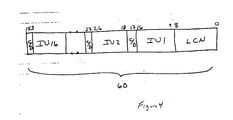
- the packet 60 has seventeen information units IU o -IU16 arranged serially as bits 0 through 153.
- the first information unit IU0 contains the logical channel number (LCN).
- Information units IU1-IU16 each contain 9-bits, e.g. bits ⁇ 7:0>, of information and a single control/data bit ⁇ 8>.
- the packet 60 is output from the m-bit computer 14 ( Figure 1) to the serial/parallel converter 30 via the high capacity serial line 16.
- the serial/parallel converter 30 provides a parallel output of the received information units on bus 48.
- the bus 48 is coupled to a 32-bit latch 34, a header latch 55 and a null detector 32.
- the header latch 55 includes a logical channel number register 36, a control/data (C/D) detect shift register 38 and a block byte counter 40.
- the logical channel number register 36, C/D detect shift register 38 and a valid information unit counter 40 are all coupled to a 32-bit receive buffer 42.
- the 32-bit latch 34 is also coupled to the 32-bit receive buffer 42.
- a block address generator 44 provides block addresses via line 56 to the receive buffer 42.
- the output from the receive buffer 42 is a five longword block which is provided to a direct memory access (DMA) controller (not shown) of the server.
- the receive buffer 42 stores the entire block before providing it to the DMA controller.
- DMA direct memory access
- a control circuit 31 is provided to enable the latch 34, registers 36, 38, 40 and receive buffer 42 to receive the proper information from the information units at proper times as described in the operation.
- the control circuit 31 receives its input from the serial bit stream 16 and provides output signals to the respective registers and latches.
- the control circuit 31 can include a bit counter which increments up to the size of each information unit and then signals an information unit counter which is incremented for each information unit received. The outputs of these counters are provided to the latches and registers of the circuit in accordance with the circuit operation.
- each information unit is provided as an input to the 32-bit latch 34, logical channel number register 36, C/D detect shift register 38 and the null detector 32. Because the first information unit, IU o , is known to contain the logical channel number, the logical channel number register 36 stores the first information unit.
- the next m-bit information unit, IU1 is then provided to the 32-bit latch 34, C/D detect shift register 38 and null detector 32.
- the C/D detect shift register 38 stores the m th bit of the information unit IU1, indicating whether the information is data or control information.
- the 32-bit latch 34 stores the information unit bits ⁇ m-1:0> in its lower ordered bit locations. Once the data from four information units IU1-IU4 have been provided to the latch 34, thus filling up the 32-bit locations, (e.g.
- the latch 34 provides the data as a single 32-bit longword output to the 32-bit receive buffer 42.
- the latch 34 stores only one information unit (bits ⁇ m-1:0>) and provides that information unit to the receive buffer 42 prior to receiving the next information unit.
- the receiver buffer 42 is thus filled with a longword of information units after four information units have been received.
- the longword is stored in an address location provided by the block address generator 44. Therefore, bits ⁇ m-1:0> of each of the information units IU1-IU4 are now stored in block locations B0-B3 as shown in Figure 2.
- the C/D detect shift register 38 shifts each control/data bit obtained from each information unit through the shift register 38 as the information units IU1-IU16 are received.
- the null detector 32 determines whether the information units contain actual information, i.e., either control or data information.
- the null detector 32 provides a signal on line 50 to the valid information unit counter 40 for each actual information unit received.
- the valid information unit counter 40 counts the number of signals from the null detector 32 to provide a count of the actual information units contained in the block 24.
- the 32-bit latch 34 provides the fourth longword of information as an input to the 32-bit receive buffer 42. Or, alternatively, the latch 34 forwards the last information unit to the receiver buffer to make up the final longword.
- the logical channel number register 36, valid information counter 40, and C/D detect shift register 38 are all filled and thus the header latch 55 is complete.
- the header latch 55 e.g.
- Each bit in the C/D bitmap 21 corresponds with an information unit BO-BF comprising the longwords stored in the receive buffer 42 and indicates whether its respective actual information unit BO-BF contains data or control information.
- the block address generator 44 must write the header information into the first address location in the block.
- the header information is output in parallel on bus 54 from the header latch 55 to the first address in the block.
- the receive buffer 42 will then contain a five longword block.
- the block of data is then output on bus 18 to the direct memory access controller for the server 12.
- the server 12 formats a fixed length block of information in an efficient data representation. If all the information units in a single block are either control, data, or null information, then by making reference to the block header for that block, the entire block of information can be processed at once by the server's processor (not shown). This greatly improves the efficiency of the server's processor which previously had to check the m th bit of each information unit received in the packet. As a result, a slower and less expensive processor can be used in the server 12.
Landscapes
- Engineering & Computer Science (AREA)
- Computer Networks & Wireless Communication (AREA)
- Signal Processing (AREA)
- Data Exchanges In Wide-Area Networks (AREA)
- Communication Control (AREA)
Applications Claiming Priority (2)
| Application Number | Priority Date | Filing Date | Title |
|---|---|---|---|
| US43803689A | 1989-11-20 | 1989-11-20 | |
| US438036 | 1989-11-20 |
Publications (3)
| Publication Number | Publication Date |
|---|---|
| EP0429055A2 true EP0429055A2 (de) | 1991-05-29 |
| EP0429055A3 EP0429055A3 (en) | 1991-12-11 |
| EP0429055B1 EP0429055B1 (de) | 1995-08-02 |
Family
ID=23738938
Family Applications (1)
| Application Number | Title | Priority Date | Filing Date |
|---|---|---|---|
| EP90122166A Expired - Lifetime EP0429055B1 (de) | 1989-11-20 | 1990-11-20 | Datenformat für Informationspakete |
Country Status (5)
| Country | Link |
|---|---|
| US (1) | US5317719A (de) |
| EP (1) | EP0429055B1 (de) |
| AU (1) | AU624274B2 (de) |
| CA (1) | CA2029390C (de) |
| DE (1) | DE69021332T2 (de) |
Cited By (6)
| Publication number | Priority date | Publication date | Assignee | Title |
|---|---|---|---|---|
| EP0637156A1 (de) * | 1993-07-30 | 1995-02-01 | Honeywell Inc. | Speicherschnittstellesystem |
| WO1995020285A1 (en) * | 1994-01-21 | 1995-07-27 | Koninklijke Ptt Nederland N.V. | Method and device for transforming a series of data packets by means of data compression |
| WO1997047116A1 (en) * | 1996-06-06 | 1997-12-11 | Advanced Micro Devices, Inc. | Data structure to support multiple transmit packets for high performance |
| GB2369540A (en) * | 2000-08-31 | 2002-05-29 | Canon Kk | Conversion between sequential data/control format and simultaneous data/control format |
| WO2003032605A1 (en) * | 2001-10-05 | 2003-04-17 | Fujitsu Limited | Method and system for communicating among heterogeneous systems |
| EP1968275A1 (de) * | 2007-03-08 | 2008-09-10 | Deutsche Telekom AG | Verfahren zur Kompaktierung von SIP-Nachrichten zur Verringerung der verbrauchten Energie bei der Kommunikation in Knoten mit begrenzten Ressourcen |
Families Citing this family (5)
| Publication number | Priority date | Publication date | Assignee | Title |
|---|---|---|---|---|
| EP0453863A2 (de) * | 1990-04-27 | 1991-10-30 | National Semiconductor Corporation | Verfahren und Gerät zur Ausführung einer Mediumzugriffssteuerung/Wirtsystemschnittstelle |
| JP3314438B2 (ja) * | 1993-02-22 | 2002-08-12 | 株式会社日立製作所 | データ通信装置 |
| KR970009698B1 (ko) * | 1994-07-07 | 1997-06-17 | 엘지산전 주식회사 | 피엘씨의 통신 파라메터 설정 방법 |
| US6567902B1 (en) * | 2000-08-15 | 2003-05-20 | Juniper Networks. Inc. | Systems and methods for packing data into a destination register |
| GB0415451D0 (en) * | 2004-07-09 | 2004-08-11 | Nokia Corp | Communication system |
Family Cites Families (23)
| Publication number | Priority date | Publication date | Assignee | Title |
|---|---|---|---|---|
| US3587044A (en) * | 1969-07-14 | 1971-06-22 | Ibm | Digital communication system |
| US3742456A (en) * | 1972-04-05 | 1973-06-26 | Pitney Bowes Inc | Apparatus for selectively formatting serial data bits into separate data characters |
| US4408272A (en) * | 1980-11-03 | 1983-10-04 | Bell Telephone Laboratories, Incorporated | Data control circuit |
| US4419728A (en) * | 1981-06-22 | 1983-12-06 | Bell Telephone Laboratories, Incorporated | Channel interface circuit providing virtual channel number translation and direct memory access |
| US4424565A (en) * | 1981-06-22 | 1984-01-03 | Bell Telephone Laboratories, Incorporated | Channel interface circuit with high speed data message header field translation and direct memory access |
| DE3265361D1 (en) * | 1981-07-10 | 1985-09-19 | Siemens Ag Albis | Bus system |
| US4554659A (en) * | 1983-12-12 | 1985-11-19 | At&T Bell Laboratories | Data communication network |
| US4536873A (en) * | 1984-03-19 | 1985-08-20 | Honeywell Inc. | Data transmission system |
| EP0162558B1 (de) * | 1984-05-21 | 1991-08-21 | Matsushita Electric Industrial Co., Ltd. | Verfahren und Vorrichtung zur Erzeugung eines lauflängenbegrenzten Kodes |
| JPS61125665A (ja) * | 1984-11-19 | 1986-06-13 | インタ−ナショナル ビジネス マシ−ンズ コ−ポレ−ション | 直列データ・リンクと入出力端末装置をインターフェースするアダプタ |
| US4916603A (en) * | 1985-03-18 | 1990-04-10 | Wang Labortatories, Inc. | Distributed reference and change table for a virtual memory system |
| US4683534A (en) * | 1985-06-17 | 1987-07-28 | Motorola, Inc. | Method and apparatus for interfacing buses of different sizes |
| US4860200A (en) * | 1985-07-03 | 1989-08-22 | Tektronix, Inc. | Microprocessor interface device for coupling non-compatible protocol peripheral with processor |
| GB8526620D0 (en) * | 1985-10-29 | 1985-12-04 | British Telecomm | Communications network |
| US4779190A (en) * | 1986-12-03 | 1988-10-18 | Ncr Corporation | Communication bus interface |
| JPS63163930A (ja) * | 1986-12-26 | 1988-07-07 | Toshiba Corp | アライメント補正方式 |
| JPS63276627A (ja) * | 1987-01-29 | 1988-11-14 | Hitachi Ltd | 印刷制御装置 |
| US4852089A (en) * | 1987-10-01 | 1989-07-25 | Data General Corporation | Methods and apparatus for allocating time slots and fragments on communications lines between adjacent nodes in a high granularity switching system |
| JP2550642B2 (ja) * | 1988-03-04 | 1996-11-06 | 日本電気株式会社 | パケットフレーム伝送方式 |
| US4949246A (en) * | 1988-06-23 | 1990-08-14 | Ncr Corporation | Adapter for transmission of data words of different lengths |
| US5068823A (en) * | 1988-07-11 | 1991-11-26 | Star Semiconductor Corporation | Programmable integrated circuit using topological and parametric data to selectively connect and configure different high level functional blocks thereof |
| US5056012A (en) * | 1988-11-30 | 1991-10-08 | Motorola, Inc. | Memory addressable data transfer network |
| US5060229A (en) * | 1989-05-12 | 1991-10-22 | Alcatel Na Network Systems Corp. | Serial transport frame format method |
-
1990
- 1990-11-01 AU AU65731/90A patent/AU624274B2/en not_active Ceased
- 1990-11-06 CA CA002029390A patent/CA2029390C/en not_active Expired - Fee Related
- 1990-11-20 DE DE69021332T patent/DE69021332T2/de not_active Expired - Lifetime
- 1990-11-20 EP EP90122166A patent/EP0429055B1/de not_active Expired - Lifetime
-
1993
- 1993-03-11 US US08/029,936 patent/US5317719A/en not_active Expired - Lifetime
Cited By (9)
| Publication number | Priority date | Publication date | Assignee | Title |
|---|---|---|---|---|
| EP0637156A1 (de) * | 1993-07-30 | 1995-02-01 | Honeywell Inc. | Speicherschnittstellesystem |
| US5864687A (en) * | 1993-07-30 | 1999-01-26 | Honeywell Inc. | Arinc 629 data receiver system having an interface for providing identification to each of the received data word types |
| WO1995020285A1 (en) * | 1994-01-21 | 1995-07-27 | Koninklijke Ptt Nederland N.V. | Method and device for transforming a series of data packets by means of data compression |
| WO1997047116A1 (en) * | 1996-06-06 | 1997-12-11 | Advanced Micro Devices, Inc. | Data structure to support multiple transmit packets for high performance |
| US5878028A (en) * | 1996-06-06 | 1999-03-02 | Advanced Micro Devices, Inc. | Data structure to support multiple transmit packets for high performance |
| GB2369540A (en) * | 2000-08-31 | 2002-05-29 | Canon Kk | Conversion between sequential data/control format and simultaneous data/control format |
| GB2369540B (en) * | 2000-08-31 | 2003-04-09 | Canon Kk | Method of transfering and formatting data and device for implementing this method |
| WO2003032605A1 (en) * | 2001-10-05 | 2003-04-17 | Fujitsu Limited | Method and system for communicating among heterogeneous systems |
| EP1968275A1 (de) * | 2007-03-08 | 2008-09-10 | Deutsche Telekom AG | Verfahren zur Kompaktierung von SIP-Nachrichten zur Verringerung der verbrauchten Energie bei der Kommunikation in Knoten mit begrenzten Ressourcen |
Also Published As
| Publication number | Publication date |
|---|---|
| EP0429055B1 (de) | 1995-08-02 |
| AU624274B2 (en) | 1992-06-04 |
| AU6573190A (en) | 1991-05-23 |
| CA2029390C (en) | 1994-12-27 |
| DE69021332D1 (de) | 1995-09-07 |
| CA2029390A1 (en) | 1991-05-21 |
| EP0429055A3 (en) | 1991-12-11 |
| DE69021332T2 (de) | 1996-04-18 |
| US5317719A (en) | 1994-05-31 |
Similar Documents
| Publication | Publication Date | Title |
|---|---|---|
| EP0429054B1 (de) | Datendarstellung und Protokoll | |
| EP0239937B1 (de) | Serielle Übertragungssteuerungsvorrichtung | |
| EP0665670B1 (de) | Verfahren und System zur Dateifernübertragung | |
| CA1320004C (en) | Hybrid communications link adapter incorporating input/output and data communications technology | |
| US5371736A (en) | Universal protocol programmable communications interface | |
| EP0429055B1 (de) | Datenformat für Informationspakete | |
| CA1315008C (en) | System permitting peripheral interchangeability | |
| EP0464716A2 (de) | Inhaltsadressierbarer Speicher | |
| US20030074502A1 (en) | Communication between two embedded processors | |
| KR880002099B1 (ko) | 메모리의 제어방식 | |
| EP0366036B1 (de) | Speicherverwaltung in Systemen mit Datenpaketbetrieb | |
| US7840741B2 (en) | System for transmitting data between two bus systems | |
| EP0072927B1 (de) | Gerät zur Speicheradressierung | |
| JP3506130B2 (ja) | バッファリング装置及びバッファリング方法 | |
| KR830008236A (ko) | 바이트 동기화를 확립하기 위해 통신 서브씨스템의 장치를 갖는 데이터 처리 씨스템 | |
| JPH09116439A (ja) | 直列データの伝送装置 | |
| JPH09154021A (ja) | 印字制御装置と印字制御方法 | |
| JPS59133638A (ja) | 端末出力方式 | |
| KR100499350B1 (ko) | 다중및단일채널을갖는다이렉트메모리억세스의데이터전송방법 | |
| JPH10105372A (ja) | データ列の圧縮装置及び圧縮方法 | |
| Parker et al. | Serial asynchronous communications between two different nuclear medicine computer systems | |
| JPH05265940A (ja) | データ転送装置 | |
| SU849191A2 (ru) | Устройство дл обмена информацией | |
| JPH0721102A (ja) | メッセージ送受信装置 | |
| JPH0580054U (ja) | データ伝送装置 |
Legal Events
| Date | Code | Title | Description |
|---|---|---|---|
| PUAI | Public reference made under article 153(3) epc to a published international application that has entered the european phase |
Free format text: ORIGINAL CODE: 0009012 |
|
| 17P | Request for examination filed |
Effective date: 19901220 |
|
| AK | Designated contracting states |
Kind code of ref document: A2 Designated state(s): DE FR GB IT |
|
| PUAL | Search report despatched |
Free format text: ORIGINAL CODE: 0009013 |
|
| AK | Designated contracting states |
Kind code of ref document: A3 Designated state(s): DE FR GB IT |
|
| 17Q | First examination report despatched |
Effective date: 19931217 |
|
| GRAA | (expected) grant |
Free format text: ORIGINAL CODE: 0009210 |
|
| AK | Designated contracting states |
Kind code of ref document: B1 Designated state(s): DE FR GB IT |
|
| REF | Corresponds to: |
Ref document number: 69021332 Country of ref document: DE Date of ref document: 19950907 |
|
| ET | Fr: translation filed | ||
| ITF | It: translation for a ep patent filed | ||
| PLBE | No opposition filed within time limit |
Free format text: ORIGINAL CODE: 0009261 |
|
| STAA | Information on the status of an ep patent application or granted ep patent |
Free format text: STATUS: NO OPPOSITION FILED WITHIN TIME LIMIT |
|
| 26N | No opposition filed | ||
| REG | Reference to a national code |
Ref country code: GB Ref legal event code: 732E |
|
| REG | Reference to a national code |
Ref country code: GB Ref legal event code: IF02 |
|
| PG25 | Lapsed in a contracting state [announced via postgrant information from national office to epo] |
Ref country code: IT Free format text: LAPSE BECAUSE OF NON-PAYMENT OF DUE FEES;WARNING: LAPSES OF ITALIAN PATENTS WITH EFFECTIVE DATE BEFORE 2007 MAY HAVE OCCURRED AT ANY TIME BEFORE 2007. THE CORRECT EFFECTIVE DATE MAY BE DIFFERENT FROM THE ONE RECORDED. Effective date: 20051120 |
|
| PGFP | Annual fee paid to national office [announced via postgrant information from national office to epo] |
Ref country code: DE Payment date: 20091127 Year of fee payment: 20 |
|
| PGFP | Annual fee paid to national office [announced via postgrant information from national office to epo] |
Ref country code: GB Payment date: 20091125 Year of fee payment: 20 Ref country code: FR Payment date: 20091201 Year of fee payment: 20 |
|
| REG | Reference to a national code |
Ref country code: GB Ref legal event code: PE20 Expiry date: 20101119 |
|
| PG25 | Lapsed in a contracting state [announced via postgrant information from national office to epo] |
Ref country code: GB Free format text: LAPSE BECAUSE OF EXPIRATION OF PROTECTION Effective date: 20101119 |
|
| PG25 | Lapsed in a contracting state [announced via postgrant information from national office to epo] |
Ref country code: DE Free format text: LAPSE BECAUSE OF EXPIRATION OF PROTECTION Effective date: 20101120 |