EP0429228B1 - Structure multicouche et méthode de construction de celle-ci pour fabriquer des modules électroluminescents à film mince émettant sur la tranche - Google Patents
Structure multicouche et méthode de construction de celle-ci pour fabriquer des modules électroluminescents à film mince émettant sur la tranche Download PDFInfo
- Publication number
- EP0429228B1 EP0429228B1 EP90312299A EP90312299A EP0429228B1 EP 0429228 B1 EP0429228 B1 EP 0429228B1 EP 90312299 A EP90312299 A EP 90312299A EP 90312299 A EP90312299 A EP 90312299A EP 0429228 B1 EP0429228 B1 EP 0429228B1
- Authority
- EP
- European Patent Office
- Prior art keywords
- layer
- stack
- electrode layer
- tfel
- bottom substrate
- Prior art date
- Legal status (The legal status is an assumption and is not a legal conclusion. Google has not performed a legal analysis and makes no representation as to the accuracy of the status listed.)
- Expired - Lifetime
Links
Images









Classifications
-
- H—ELECTRICITY
- H05—ELECTRIC TECHNIQUES NOT OTHERWISE PROVIDED FOR
- H05B—ELECTRIC HEATING; ELECTRIC LIGHT SOURCES NOT OTHERWISE PROVIDED FOR; CIRCUIT ARRANGEMENTS FOR ELECTRIC LIGHT SOURCES, IN GENERAL
- H05B33/00—Electroluminescent light sources
- H05B33/12—Light sources with substantially two-dimensional [2D] radiating surfaces
-
- H—ELECTRICITY
- H05—ELECTRIC TECHNIQUES NOT OTHERWISE PROVIDED FOR
- H05B—ELECTRIC HEATING; ELECTRIC LIGHT SOURCES NOT OTHERWISE PROVIDED FOR; CIRCUIT ARRANGEMENTS FOR ELECTRIC LIGHT SOURCES, IN GENERAL
- H05B33/00—Electroluminescent light sources
- H05B33/10—Apparatus or processes specially adapted to the manufacture of electroluminescent light sources
Definitions
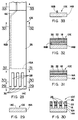
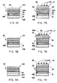
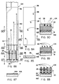
- Fig. 52 is a fragmentary plan view of a partially constructed TFEL structure illustrating the series of bus bar conductors of Fig. 51 applied over the lower insulation layer at the crossover section of the partially constructed TFEL structure of Fig. 45.
Landscapes
- Engineering & Computer Science (AREA)
- Manufacturing & Machinery (AREA)
- Electroluminescent Light Sources (AREA)
Claims (6)
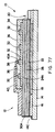
- Structure multi-couches destinée à produire un module électroluminescent, à couches minces et émettant par la tranche, qui comprend:(a) une couche formant substrat de base qui comporte un bord antérieur,(b) un empilement électroluminescent (EL) recouvrant ladite couche formant substrat de base et comportant une partie antérieure et au moins un couche intermédiaire qui produit de l'énergie lumineuse,(c) une couche inférieure formant électrode, intercalée entre ladite couche formant substrat de base et ledit empilement EL et comportant une partie antérieure, lesdites parties antérieures dudit empilement EL et de ladite couche inférieure formant électrode comportant une série de canaux longitudinaux qui les traversent jusqu'à la profondeur de ladite couche formant substrat de base et une voie transversale qui relie lesdits canaux et qui s'étend le long dudit bord antérieur de ladite couche formant substrat de base de manière à définir une pluralité d'éléments longitudinaux transversalement espacés, et(d) une couche supérieure formant électrode comportant une partie antérieure composée d'une pluralité d'électrodes longitudinales transversalement espacées, lesdites électrodes longitudinales de ladite partie antérieure de ladite couche supérieure formant électrode recouvrant lesdits éléments longitudinaux desdites parties antérieures de l'empilement EL et de la couche inférieure formant électrode de manière à définir avec eux une pluralité de pixels ayant des bords antérieurs d'émission de lumière qui sont en retrait de la largeur de ladite voie par rapport audit bord antérieur de ladite couche formant substrat de base.
- Structure selon la revendication 1, dans laquelle ledit empilement EL contient au moins une couche diélectrique intercalée entre lesdites couches supérieure et inférieure formant électrodes.
- Structure selon la revendication 2, dans laquelle ladite couche produisant de l'énergie lumineuse est intercalée entre ladite couche diélectrique et ladite couche supérieure ou inférieure formant électrode.
- Structure selon la revendication 3, dans laquelle ladite couche produisant de l'énergie lumineuse est une couche de matériau électoluminescent.
- Procédé de fabrication d'une structure multi-couches destinée à produire un module électroluminescent, à couches minces et émettant par la tranche, ledit procédé comprenant les étapes consistant à :(a) former une couche inférieure formant électrode sur une couche formant substrat de base,(b) former un empilement électroluminescent (EL) sur la couche inférieure formant électrode, ledit empilement comportant au moins une couche intermédiaire qui produit de l'énergie lumineuse, et(c) former une série de canaux longitudinaux et une voie transversale, qui relie ces canaux et s'étend le long d'un bord antérieur de la couche formant substrat de base, dans des parties antérieures de l'empilement EL et de la couche inférieure formant électrode de manière à définir une pluralité d'éléments longitudinaux transversalement espacés sur les parties antérieures de l'empilement EL et de la couche inférieure formant électrode qui ont des bords antérieurs d'émission de lumière qui sont en retrait de la largeur de ladite voie par rapport au bord antérieur de la couche formant substrat de base.
- Procédé selon la revendication 5, comprenant en outre l'étape qui consiste à former une couche supérieure formant électrode, faite d'une pluralité d'électrodes longitudinales transversalement espacées, sur l'empilement EL, la partie antérieure des électrodes longitudinales recouvrant les éléments longitudinaux sur les parties antérieures de l'empilement EL et de la couche inférieure formant électrode.
Applications Claiming Priority (2)
| Application Number | Priority Date | Filing Date | Title |
|---|---|---|---|
| US07/434,397 US5118987A (en) | 1989-11-13 | 1989-11-13 | Multi-layer structure and method of constructing the same for providing tfel edge emitter modules |
| US434397 | 1989-11-13 |
Publications (3)
| Publication Number | Publication Date |
|---|---|
| EP0429228A2 EP0429228A2 (fr) | 1991-05-29 |
| EP0429228A3 EP0429228A3 (en) | 1992-03-11 |
| EP0429228B1 true EP0429228B1 (fr) | 1995-04-26 |
Family
ID=23724072
Family Applications (1)
| Application Number | Title | Priority Date | Filing Date |
|---|---|---|---|
| EP90312299A Expired - Lifetime EP0429228B1 (fr) | 1989-11-13 | 1990-11-09 | Structure multicouche et méthode de construction de celle-ci pour fabriquer des modules électroluminescents à film mince émettant sur la tranche |
Country Status (5)
| Country | Link |
|---|---|
| US (1) | US5118987A (fr) |
| EP (1) | EP0429228B1 (fr) |
| JP (1) | JPH03208299A (fr) |
| CA (1) | CA2029028A1 (fr) |
| DE (1) | DE69018936T2 (fr) |
Families Citing this family (9)
| Publication number | Priority date | Publication date | Assignee | Title |
|---|---|---|---|---|
| US5184969A (en) * | 1988-05-31 | 1993-02-09 | Electroluminscent Technologies Corporation | Electroluminescent lamp and method for producing the same |
| US5504390A (en) * | 1994-03-03 | 1996-04-02 | Topp; Mark | Addressable electroluminescent display panel having a continuous footprint |
| US6104041A (en) * | 1994-08-24 | 2000-08-15 | Sarnoff Corporation | Switching circuitry layout for an active matrix electroluminescent display pixel with each pixel provided with the transistors |
| US5587329A (en) * | 1994-08-24 | 1996-12-24 | David Sarnoff Research Center, Inc. | Method for fabricating a switching transistor having a capacitive network proximate a drift region |
| US5525866A (en) * | 1995-01-06 | 1996-06-11 | Mueller; Gerd O. | Edge emitter as a directional line source |
| US5598067A (en) * | 1995-06-07 | 1997-01-28 | Vincent; Kent | Electroluminescent device as a source for a scanner |
| US5949188A (en) * | 1996-12-18 | 1999-09-07 | Hage Gmbh & Co. Kg | Electroluminescent display device with continuous base electrode |
| WO1999027555A1 (fr) * | 1997-11-26 | 1999-06-03 | Stapleton Robert E | Afficheur a ecran plat ayant une surface d'image en contact avec les bords d'ecran |
| JP3718770B2 (ja) * | 2002-01-11 | 2005-11-24 | 株式会社日立製作所 | アクティブマトリックス型の表示装置 |
Family Cites Families (4)
| Publication number | Priority date | Publication date | Assignee | Title |
|---|---|---|---|---|
| US4535341A (en) * | 1983-08-19 | 1985-08-13 | Westinghouse Electric Corp. | Thin film electroluminescent line array emitter and printer |
| US5004556A (en) * | 1987-06-17 | 1991-04-02 | Colgate-Palmolive Company | Built thickened stable non-aqueous cleaning composition and method of use |
| US5004956A (en) * | 1988-08-23 | 1991-04-02 | Westinghouse Electric Corp. | Thin film electroluminescent edge emitter structure on a silcon substrate |
| US4899184A (en) * | 1989-04-24 | 1990-02-06 | Westinghouse Electric Corp. | Multiplexed thin film electroluminescent edge emitter structure and electronic drive system therefrom |
-
1989
- 1989-11-13 US US07/434,397 patent/US5118987A/en not_active Expired - Fee Related
-
1990
- 1990-10-29 JP JP2291677A patent/JPH03208299A/ja active Pending
- 1990-10-31 CA CA002029028A patent/CA2029028A1/fr not_active Abandoned
- 1990-11-09 EP EP90312299A patent/EP0429228B1/fr not_active Expired - Lifetime
- 1990-11-09 DE DE69018936T patent/DE69018936T2/de not_active Expired - Fee Related
Also Published As
| Publication number | Publication date |
|---|---|
| US5118987A (en) | 1992-06-02 |
| DE69018936D1 (de) | 1995-06-01 |
| EP0429228A2 (fr) | 1991-05-29 |
| JPH03208299A (ja) | 1991-09-11 |
| DE69018936T2 (de) | 1995-12-21 |
| EP0429228A3 (en) | 1992-03-11 |
| CA2029028A1 (fr) | 1991-05-14 |
Similar Documents
| Publication | Publication Date | Title |
|---|---|---|
| US4665342A (en) | Screen printable polymer electroluminescent display with isolation | |
| US5118987A (en) | Multi-layer structure and method of constructing the same for providing tfel edge emitter modules | |
| JP2002117975A (ja) | 単純マトリクス式画素配列型有機電界発光装置の製造方法 | |
| US5465024A (en) | Flat panel display using field emission devices | |
| JP3066573B2 (ja) | 電界放出型表示素子 | |
| US5403614A (en) | Method for making an electroluminescent element | |
| US5872421A (en) | Surface electron display device with electron sink | |
| US6045426A (en) | Method to manufacture field emission array with self-aligned focus structure | |
| JP2001267085A (ja) | 有機発光装置およびその製造方法 | |
| EP0706198B1 (fr) | Source d'électrons à conducteurs redondants | |
| US4733139A (en) | Fluorescent display device | |
| EP0706197B1 (fr) | Source d'électrons | |
| US6015324A (en) | Fabrication process for surface electron display device with electron sink | |
| GB2151077A (en) | Polychromatic electroluminescent panel | |
| KR940008008Y1 (ko) | 형광표시관 | |
| EP0393979A2 (fr) | Méthode de fabrication de rangées de dispositifs électroluminescents à émission latérale | |
| KR100338031B1 (ko) | 이중 그리드 전극을 갖는 형광표시관 | |
| KR970005102B1 (ko) | 박막형 전장 발광 표시소자 | |
| KR900006800B1 (ko) | 직류 구동형 el 평면소자 | |
| JPH11195493A (ja) | 有機el素子とその駆動方法 | |
| JPH0119840Y2 (fr) | ||
| JPS60160549A (ja) | 螢光表示管 | |
| JPH0325895A (ja) | エレクトロルミネッセンス表示素子及びその製造方法 | |
| JPH0817578A (ja) | 薄膜電場発光素子 | |
| JPH0589960A (ja) | 薄膜el素子 |
Legal Events
| Date | Code | Title | Description |
|---|---|---|---|
| PUAI | Public reference made under article 153(3) epc to a published international application that has entered the european phase |
Free format text: ORIGINAL CODE: 0009012 |
|
| AK | Designated contracting states |
Kind code of ref document: A2 Designated state(s): DE FR GB IT |
|
| PUAL | Search report despatched |
Free format text: ORIGINAL CODE: 0009013 |
|
| AK | Designated contracting states |
Kind code of ref document: A3 Designated state(s): DE FR GB IT |
|
| 17P | Request for examination filed |
Effective date: 19920707 |
|
| 17Q | First examination report despatched |
Effective date: 19931119 |
|
| GRAA | (expected) grant |
Free format text: ORIGINAL CODE: 0009210 |
|
| AK | Designated contracting states |
Kind code of ref document: B1 Designated state(s): DE FR GB IT |
|
| ET | Fr: translation filed | ||
| REF | Corresponds to: |
Ref document number: 69018936 Country of ref document: DE Date of ref document: 19950601 |
|
| ITF | It: translation for a ep patent filed | ||
| PLBE | No opposition filed within time limit |
Free format text: ORIGINAL CODE: 0009261 |
|
| STAA | Information on the status of an ep patent application or granted ep patent |
Free format text: STATUS: NO OPPOSITION FILED WITHIN TIME LIMIT |
|
| 26N | No opposition filed | ||
| PGFP | Annual fee paid to national office [announced via postgrant information from national office to epo] |
Ref country code: DE Payment date: 19961128 Year of fee payment: 7 |
|
| PGFP | Annual fee paid to national office [announced via postgrant information from national office to epo] |
Ref country code: GB Payment date: 19971007 Year of fee payment: 8 |
|
| PGFP | Annual fee paid to national office [announced via postgrant information from national office to epo] |
Ref country code: FR Payment date: 19971106 Year of fee payment: 8 |
|
| PG25 | Lapsed in a contracting state [announced via postgrant information from national office to epo] |
Ref country code: DE Free format text: LAPSE BECAUSE OF NON-PAYMENT OF DUE FEES Effective date: 19980901 |
|
| PG25 | Lapsed in a contracting state [announced via postgrant information from national office to epo] |
Ref country code: GB Free format text: LAPSE BECAUSE OF NON-PAYMENT OF DUE FEES Effective date: 19981109 |
|
| GBPC | Gb: european patent ceased through non-payment of renewal fee |
Effective date: 19981109 |
|
| PG25 | Lapsed in a contracting state [announced via postgrant information from national office to epo] |
Ref country code: FR Free format text: LAPSE BECAUSE OF NON-PAYMENT OF DUE FEES Effective date: 19990730 |
|
| REG | Reference to a national code |
Ref country code: FR Ref legal event code: ST |
|
| PG25 | Lapsed in a contracting state [announced via postgrant information from national office to epo] |
Ref country code: IT Free format text: LAPSE BECAUSE OF NON-PAYMENT OF DUE FEES;WARNING: LAPSES OF ITALIAN PATENTS WITH EFFECTIVE DATE BEFORE 2007 MAY HAVE OCCURRED AT ANY TIME BEFORE 2007. THE CORRECT EFFECTIVE DATE MAY BE DIFFERENT FROM THE ONE RECORDED. Effective date: 20051109 |