EP0429889A2 - Transmission d'un signal auxiliaire dans un système de transmission pour signaux numÀ©riques à grand débit - Google Patents
Transmission d'un signal auxiliaire dans un système de transmission pour signaux numÀ©riques à grand débit Download PDFInfo
- Publication number
- EP0429889A2 EP0429889A2 EP90121128A EP90121128A EP0429889A2 EP 0429889 A2 EP0429889 A2 EP 0429889A2 EP 90121128 A EP90121128 A EP 90121128A EP 90121128 A EP90121128 A EP 90121128A EP 0429889 A2 EP0429889 A2 EP 0429889A2
- Authority
- EP
- European Patent Office
- Prior art keywords
- bit
- zero
- bits
- binary
- sequence
- Prior art date
- Legal status (The legal status is an assumption and is not a legal conclusion. Google has not performed a legal analysis and makes no representation as to the accuracy of the status listed.)
- Granted
Links
Images
Classifications
-
- H—ELECTRICITY
- H04—ELECTRIC COMMUNICATION TECHNIQUE
- H04L—TRANSMISSION OF DIGITAL INFORMATION, e.g. TELEGRAPHIC COMMUNICATION
- H04L25/00—Baseband systems
- H04L25/38—Synchronous or start-stop systems, e.g. for Baudot code
- H04L25/40—Transmitting circuits; Receiving circuits
- H04L25/49—Transmitting circuits; Receiving circuits using code conversion at the transmitter; using predistortion; using insertion of idle bits for obtaining a desired frequency spectrum; using three or more amplitude levels ; Baseband coding techniques specific to data transmission systems
- H04L25/4906—Transmitting circuits; Receiving circuits using code conversion at the transmitter; using predistortion; using insertion of idle bits for obtaining a desired frequency spectrum; using three or more amplitude levels ; Baseband coding techniques specific to data transmission systems using binary codes
- H04L25/4908—Transmitting circuits; Receiving circuits using code conversion at the transmitter; using predistortion; using insertion of idle bits for obtaining a desired frequency spectrum; using three or more amplitude levels ; Baseband coding techniques specific to data transmission systems using binary codes using mBnB codes
- H04L25/491—Transmitting circuits; Receiving circuits using code conversion at the transmitter; using predistortion; using insertion of idle bits for obtaining a desired frequency spectrum; using three or more amplitude levels ; Baseband coding techniques specific to data transmission systems using binary codes using mBnB codes using 1B2B codes
- H04L25/4912—Transmitting circuits; Receiving circuits using code conversion at the transmitter; using predistortion; using insertion of idle bits for obtaining a desired frequency spectrum; using three or more amplitude levels ; Baseband coding techniques specific to data transmission systems using binary codes using mBnB codes using 1B2B codes using CMI or 2-HDB-3 code
Definitions
- the invention relates to a method for the additional transmission of a digital signal according to the preamble of claim 1.
- a transmission system for digital signals of high walking speed is known, in which a signal of comparatively low walking speed is also transmitted.
- the known transmission system contains code converters in the line terminals which convert the digital signal to be transmitted into the actual transmission code, in particular into a 4B 3T code or a 5B 6B code on the transmission side and reset on the reception side.
- the required clock signal is generated by means of a phase-locked loop and the control voltage of the phase-locked loop is additionally amplitude-modulated to transmit the additional signal and thus phase-modulated the signals delivered to the line via the clock signal.
- phase discriminator contained in the phase-locked loop for clock generation also acts as a demodulator for the additional signals that can be taken from the phase discriminator output.
- the transmission capacity for an additional signal is limited in this prior art, since a phase shift that is too large would produce considerable undesirable jitter, which would then require additional effort for eliminating the jitter or the effects on the useful signal transmission.
- phase modulation is undesirable since it can only be generated with digital modules in rare cases.
- the object of the invention is therefore to develop a method of the type mentioned at the outset in such a way that there is a higher transmission capacity for an additional signal and the process can be implemented with digital and thus easily integrated modules.
- it must be ensured that the transmission of the digital useful signals continues to be error-free, and the reception-side generation of a clock signal from the received transmission signals must continue to be possible with the required accuracy.
- the object is achieved by a method of the type mentioned at the outset, which is further developed by the features of the characterizing part of patent claim 1.
- a particular advantage of the method according to the invention is the possibility of being able to distinguish normal transmission errors from the artificially inserted code rule violations, so that the frequency of errors in the digital useful signal can still be measured at the end of the transmission path.
- Two alternative options for developing the method according to the invention are described in more detail in claims 2 and 3, while in claims 4 to 6 a preferred embodiment of the method according to the invention is described in detail.
- the transmission signals in the CMI code are usually generated from binary signals by transcoding.
- a binary zero character is converted during the encoding into an element combination consisting of a zero bit and a one-bit, while a binary one character during the encoding, if the last binary one character was encoded as a double zero character, into a double one character and, if the last binary one character as a double one character was encoded, converted to a double zero character.
- This assignment or the characters are changed when a one-bit begins in the additional signal to be transmitted. Instead of the start of a one-bit of the additional signal, the start of a zero bit could also be selected, but the start of a one-bit is easier to recognize, so that this variant was preferred in the exemplary embodiment.
- the code rule violation is not restricted to one element combination in the CMI code, but a first prohibited element combination, i.e. the CMI, becomes available when a one bit of the additional signal begins Code rule contradicts, sent out, followed by a first regular element combination and a second prohibited element combination.
- a characteristic double violation of the CMI code which includes a regular element combination.
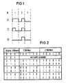
- FIG. 1 in the top line labeled B, a bit sequence consisting of three binary characters is shown, which is to be recoded into the CMI code.
- the line labeled C1 shows the impulses that occur during regular recoding into the CMI code, assuming was that the last recoded binary one bit was reproduced with a double zero bit in the CMI code.
- the element combinations 110100 result in the CMI code, whereby, as can be seen, NRZ signals were assumed, and the pulses in each case fill the entire length of the element in the CMI code, comparable full-bit-wide signals in the binary code.
- Received element combinations are shown in the line labeled C2, the second element being falsified by a transmission error in the first element combination.
- This transmission error is easily recognizable at the receiving end, since binary one bits are only reproduced as double ones or double zero element combinations and a binary zero bit is only represented by a zero-one element combination.
- the zero-one element combination generated by the transmission error is not included in the intended CMI code and can therefore be recognized as a transmission error.
- a double code rule violation to mark the beginning of a one-bit of the additional signal was deliberately shown when the binary string B was recoded.
- the double zero element combination corresponds to the element combination intended for a binary one-bit, because of the assumed history - the last binary one should have been coded as a double zero element combination - the CMI code rule was violated with the first element combination.
- the second element combination corresponds to the CMI code rule, so that there is no code rule violation.
- a double zero element combination was again generated as the third element combination, although the first double zero element combination should have been followed by a double one element combination with regular recoding. It can thus be seen at the receiving end that there is a second code rule violation, that is to say a total of a regular element combination is enclosed by two irregular element combinations.
- FIG. 2 shows a diagram for the additional signal insertion when transcoding binary three-bit words into CMI words consisting of three element combinations.
- the schema results from assigning a clear binary signal content to the element combinations prohibited by the CMI code rule, instead of a single violation of the CMI code rule by performing a double violation in such a way that the occurrence of this double violation: violation of the CMI code rule - Non-violation - violation - so that a pretense of transmission errors is extremely unlikely and that only the beginning of each one bit of the additional channel is marked in the manner described.
- the binary three bit words are each assigned a first and a second CMI code word; the first CMI code word is generated if the last one in the CMI code was reproduced with a double zero bit, accordingly the second CMI word is generated if the immediately preceding last one in the CMI code was reproduced with a double one bit.
- a digital useful signal consisting of a sequence of three binary zero bits results as the first and second CMI word in the same sequence from one one bit, two zero bits, two one bits and one zero bit.
- a binary three-bit word consisting of a sequence of two zero bits and one one-bit is not provided, so that no CMI words have been provided for this.
- a binary three-bit word consisting of a sequence of one zero bit, one one-bit and one zero bit results in a sequence of one one-bit, one zero bit, three one-bit and one zero-bit as the first CMI word and one sequence of one one-bit, three as the second CMI word Zero bit, one bit and one zero bit.
- a binary three-bit word consisting of a sequence of one zero bit and two one bits results in a sequence of one one bit, one zero bit and four one bits as the first CMI word and one sequence as the second CMI word from one bit and five zero bits.
- a binary three-bit word consisting of a sequence of one bit and two zero bits results in a sequence of three zero bits, two one bits and one zero bit as the first CMI word and a sequence of two one bits, one zero bit, two one bits and as the second CMI word a zero bit.
- a binary three-bit word consisting of a sequence of one bit, one zero bit and one one bit results in a sequence of three zero bits, one one bit and two zero bits as the first CMI word and a sequence of two one bits, one zero bit and as the second CMI word three one bits.
- a binary three-bit word consisting of a sequence of two one-bit and one zero bit results in a sequence of two zero bits, three one-bit and one zero bit as the first CMI word and a sequence of two one-bit, two zero bit, one one bit and as the second CMI word a zero bit and a binary three-bit word consisting of three one bits results in a sequence of two zero bits and four one bits as the first CMI word and a sequence of two one bits and four zero bits as the second CMI word. If the binary three-bit word consisting of a sequence of two zero bits and one one-bit is present, the beginning of a one-bit of the additional signal is not shown immediately, but only with the next bit of the digital useful signal.
- the then existing three-bit word begins with the permitted combination of zero and one and thus enables the additional signal to be faded in in the manner described.
- the reason for the non-use of the binary three-bit word consisting of two zeros and a one for the overlay is that the application of the special violation rule described leads to the formation of CMI code elements, which also result from a single transmission error from a regular CMI Signal can arise.
Landscapes
- Physics & Mathematics (AREA)
- Spectroscopy & Molecular Physics (AREA)
- Engineering & Computer Science (AREA)
- Computer Networks & Wireless Communication (AREA)
- Signal Processing (AREA)
- Dc Digital Transmission (AREA)
- Digital Transmission Methods That Use Modulated Carrier Waves (AREA)
- Reduction Or Emphasis Of Bandwidth Of Signals (AREA)
- Time-Division Multiplex Systems (AREA)
- Synchronisation In Digital Transmission Systems (AREA)
Applications Claiming Priority (2)
| Application Number | Priority Date | Filing Date | Title |
|---|---|---|---|
| DE3939640 | 1989-11-30 | ||
| DE3939640 | 1989-11-30 |
Publications (3)
| Publication Number | Publication Date |
|---|---|
| EP0429889A2 true EP0429889A2 (fr) | 1991-06-05 |
| EP0429889A3 EP0429889A3 (en) | 1992-12-23 |
| EP0429889B1 EP0429889B1 (fr) | 1995-11-08 |
Family
ID=6394523
Family Applications (1)
| Application Number | Title | Priority Date | Filing Date |
|---|---|---|---|
| EP90121128A Expired - Lifetime EP0429889B1 (fr) | 1989-11-30 | 1990-11-05 | Transmission d'un signal auxiliaire dans un système de transmission pour signaux numériques à grand débit |
Country Status (4)
| Country | Link |
|---|---|
| EP (1) | EP0429889B1 (fr) |
| AT (1) | ATE130146T1 (fr) |
| AU (1) | AU627383B2 (fr) |
| DE (1) | DE59009855D1 (fr) |
Cited By (1)
| Publication number | Priority date | Publication date | Assignee | Title |
|---|---|---|---|---|
| CN101674108B (zh) * | 2008-09-08 | 2013-03-27 | 索尼株式会社 | 信息处理装置、编码方法和信号传输方法 |
Families Citing this family (2)
| Publication number | Priority date | Publication date | Assignee | Title |
|---|---|---|---|---|
| EP0433706B1 (fr) * | 1989-12-18 | 1995-04-26 | Siemens Aktiengesellschaft | Transmission d'un signal auxiliaire dans un système de communication pour signaux numériques à grand débit |
| ATE122516T1 (de) * | 1989-12-18 | 1995-05-15 | Siemens Ag | Empfänger für ein digitales zusatzsignal in einem digitalen übertragungssystem. |
Family Cites Families (5)
| Publication number | Priority date | Publication date | Assignee | Title |
|---|---|---|---|---|
| DE3412986A1 (de) * | 1984-04-06 | 1985-10-24 | Standard Elektrik Lorenz Ag, 7000 Stuttgart | Digitales nachrichtenuebertragungssystem mit integrierter uebertragung einer zusatzinformation mit geringer bitfolgefrequenz |
| CH666150A5 (de) * | 1984-09-28 | 1988-06-30 | Bbc Brown Boveri & Cie | Verfahren zur zusaetzlichen uebertragung von informationen ueber einen digitalen hilfskanal sowie anwendung des verfahrens. |
| DE3723187A1 (de) * | 1987-07-14 | 1989-01-26 | Philips Patentverwaltung | Digitales nachrichtenuebertragungssystem |
| EP0433706B1 (fr) * | 1989-12-18 | 1995-04-26 | Siemens Aktiengesellschaft | Transmission d'un signal auxiliaire dans un système de communication pour signaux numériques à grand débit |
| ATE122516T1 (de) * | 1989-12-18 | 1995-05-15 | Siemens Ag | Empfänger für ein digitales zusatzsignal in einem digitalen übertragungssystem. |
-
1990
- 1990-11-05 AT AT90121128T patent/ATE130146T1/de not_active IP Right Cessation
- 1990-11-05 DE DE59009855T patent/DE59009855D1/de not_active Expired - Fee Related
- 1990-11-05 EP EP90121128A patent/EP0429889B1/fr not_active Expired - Lifetime
- 1990-11-29 AU AU67099/90A patent/AU627383B2/en not_active Ceased
Cited By (1)
| Publication number | Priority date | Publication date | Assignee | Title |
|---|---|---|---|---|
| CN101674108B (zh) * | 2008-09-08 | 2013-03-27 | 索尼株式会社 | 信息处理装置、编码方法和信号传输方法 |
Also Published As
| Publication number | Publication date |
|---|---|
| EP0429889B1 (fr) | 1995-11-08 |
| ATE130146T1 (de) | 1995-11-15 |
| AU6709990A (en) | 1991-06-06 |
| EP0429889A3 (en) | 1992-12-23 |
| DE59009855D1 (de) | 1995-12-14 |
| AU627383B2 (en) | 1992-08-20 |
Similar Documents
| Publication | Publication Date | Title |
|---|---|---|
| DE69319997T2 (de) | Modulationsverfahren, Modulationsvorrichtung und Demodulationsvorrichtung | |
| DE69626350T2 (de) | Aufzeichnungsmedium, digitale modulations/demodulationsvorrichtung und digitale modulations/demodulationsverfahren | |
| DE3125529C2 (de) | Verfahren zum Umkodieren einer Folge von Datenbits in eine Folge von Kanalbits, Anordnung zum Dekodieren der nach diesem Verfahren kodierten Kanalbits und Aufzeichnungsträger mit einer gemäß diesem Verfahren erzeugten Informationsstruktur | |
| DE69425298T2 (de) | Einrichtung zur Kodierung/Dekodierung von n-bit Quellworten in entsprechende m-bit Kanalworte und umgekehrt | |
| DE2944459A1 (de) | Verfahren zum uebertragen von digitalsignalen mittels signalgeber | |
| DE4344811B4 (de) | Faltungscodierer und gittercodierte Modulationsvorrichtung mit einem Faltungscodierer | |
| DE3147578C2 (fr) | ||
| DE69032076T2 (de) | Einrichtung für Datenkodierung und Vorwärts-Fehlerkorrektur für eine niedrige Offset-Gleichspannung und eine kurze Lauflänge | |
| DE69329740T2 (de) | Miller-Quadratdekoder mit Löschfahnenausgang | |
| DE3000941C2 (de) | Anordnung zur Übertragung zusätzlicher Informationen für eine Einrichtung zur Übertragung digitaler Daten | |
| EP0464910A2 (fr) | Dispositif de transmission à canal principal codé en blocs et à canal additionnel | |
| DE19643502A1 (de) | Verfahren zur Decodierung eines digitalen Signals, Bussystem und Peripheriegerät hierfür | |
| EP0429889B1 (fr) | Transmission d'un signal auxiliaire dans un système de transmission pour signaux numériques à grand débit | |
| DE3500115A1 (de) | Verfahren zum codieren eines datenbitmusters, anordnung zur durchfuehrung des verfahrens und anordnung zum decodieren des mit dem verfahren erhaltenen kanalbitflusses | |
| DE69933499T2 (de) | Verfahren und Einrichtung zur Übertragung eines gleichstromfreien Mehrfachpegelkodes | |
| DE2203415B2 (de) | Verfahren zum Kodieren eines binare Information fuhrenden Datenflusses und Anlage zur Durchfuhrung dieses Verfahrens | |
| DE3529435C2 (fr) | ||
| DE2047254C3 (fr) | ||
| DE69124242T2 (de) | Verfahren und anordnung zur beschränkung des bandpasses binärer signale | |
| EP0051725A1 (fr) | Procédé de transmission pour signaux numériques | |
| DE3718632C1 (de) | Verfahren zur Dekodierung von Daten | |
| DE3331514A1 (de) | Verfahren zum codieren eines datenbitflusses, anordnung zum durchfuehren des verfahrens und anordnung zum decodieren eines datenflusses | |
| DE2648027C3 (de) | Verfahren zur Datenübertragung im Start-Stop-Betrieb | |
| DE2915067C2 (de) | Verfahren zur Redundanzreduktion bei der Übertragung digital codierter Analogsignale | |
| DE2426769C3 (de) | Verfahren zur Übertragung digitaler Signale mit Fehlersicherung |
Legal Events
| Date | Code | Title | Description |
|---|---|---|---|
| PUAI | Public reference made under article 153(3) epc to a published international application that has entered the european phase |
Free format text: ORIGINAL CODE: 0009012 |
|
| 17P | Request for examination filed |
Effective date: 19901205 |
|
| AK | Designated contracting states |
Kind code of ref document: A2 Designated state(s): AT BE CH DE ES FR GB GR IT LI NL SE |
|
| PUAL | Search report despatched |
Free format text: ORIGINAL CODE: 0009013 |
|
| AK | Designated contracting states |
Kind code of ref document: A3 Designated state(s): AT BE CH DE ES FR GB GR IT LI NL SE |
|
| 17Q | First examination report despatched |
Effective date: 19940927 |
|
| GRAA | (expected) grant |
Free format text: ORIGINAL CODE: 0009210 |
|
| AK | Designated contracting states |
Kind code of ref document: B1 Designated state(s): AT BE CH DE ES FR GB GR IT LI NL SE |
|
| PG25 | Lapsed in a contracting state [announced via postgrant information from national office to epo] |
Ref country code: IT Free format text: LAPSE BECAUSE OF FAILURE TO SUBMIT A TRANSLATION OF THE DESCRIPTION OR TO PAY THE FEE WITHIN THE PRESCRIBED TIME-LIMIT;WARNING: LAPSES OF ITALIAN PATENTS WITH EFFECTIVE DATE BEFORE 2007 MAY HAVE OCCURRED AT ANY TIME BEFORE 2007. THE CORRECT EFFECTIVE DATE MAY BE DIFFERENT FROM THE ONE RECORDED. Effective date: 19951108 Ref country code: GB Effective date: 19951108 Ref country code: ES Free format text: THE PATENT HAS BEEN ANNULLED BY A DECISION OF A NATIONAL AUTHORITY Effective date: 19951108 Ref country code: GR Free format text: LAPSE BECAUSE OF FAILURE TO SUBMIT A TRANSLATION OF THE DESCRIPTION OR TO PAY THE FEE WITHIN THE PRESCRIBED TIME-LIMIT Effective date: 19951108 Ref country code: BE Effective date: 19951108 Ref country code: FR Effective date: 19951108 |
|
| REF | Corresponds to: |
Ref document number: 130146 Country of ref document: AT Date of ref document: 19951115 Kind code of ref document: T |
|
| REF | Corresponds to: |
Ref document number: 59009855 Country of ref document: DE Date of ref document: 19951214 |
|
| PG25 | Lapsed in a contracting state [announced via postgrant information from national office to epo] |
Ref country code: SE Effective date: 19960208 |
|
| REG | Reference to a national code |
Ref country code: CH Ref legal event code: NV Representative=s name: SIEMENS-ALBIS AKTIENGESELLSCHAFT |
|
| EN | Fr: translation not filed | ||
| GBV | Gb: ep patent (uk) treated as always having been void in accordance with gb section 77(7)/1977 [no translation filed] |
Effective date: 19951108 |
|
| PLBE | No opposition filed within time limit |
Free format text: ORIGINAL CODE: 0009261 |
|
| PGFP | Annual fee paid to national office [announced via postgrant information from national office to epo] |
Ref country code: AT Payment date: 19961025 Year of fee payment: 7 |
|
| 26N | No opposition filed | ||
| PGFP | Annual fee paid to national office [announced via postgrant information from national office to epo] |
Ref country code: NL Payment date: 19961118 Year of fee payment: 7 |
|
| PG25 | Lapsed in a contracting state [announced via postgrant information from national office to epo] |
Ref country code: CH Effective date: 19961130 Ref country code: LI Effective date: 19961130 |
|
| REG | Reference to a national code |
Ref country code: CH Ref legal event code: PL |
|
| PG25 | Lapsed in a contracting state [announced via postgrant information from national office to epo] |
Ref country code: AT Free format text: LAPSE BECAUSE OF NON-PAYMENT OF DUE FEES Effective date: 19971105 |
|
| PG25 | Lapsed in a contracting state [announced via postgrant information from national office to epo] |
Ref country code: NL Free format text: LAPSE BECAUSE OF NON-PAYMENT OF DUE FEES Effective date: 19980601 |
|
| NLV4 | Nl: lapsed or anulled due to non-payment of the annual fee |
Effective date: 19980601 |
|
| PGFP | Annual fee paid to national office [announced via postgrant information from national office to epo] |
Ref country code: DE Payment date: 19990120 Year of fee payment: 9 |
|
| PG25 | Lapsed in a contracting state [announced via postgrant information from national office to epo] |
Ref country code: DE Free format text: LAPSE BECAUSE OF NON-PAYMENT OF DUE FEES Effective date: 20000901 |