EP0430236B1 - Amplificateur de puissance - Google Patents
Amplificateur de puissance Download PDFInfo
- Publication number
- EP0430236B1 EP0430236B1 EP90122849A EP90122849A EP0430236B1 EP 0430236 B1 EP0430236 B1 EP 0430236B1 EP 90122849 A EP90122849 A EP 90122849A EP 90122849 A EP90122849 A EP 90122849A EP 0430236 B1 EP0430236 B1 EP 0430236B1
- Authority
- EP
- European Patent Office
- Prior art keywords
- circuit
- amplifier
- standby
- power
- power amplifier
- Prior art date
- Legal status (The legal status is an assumption and is not a legal conclusion. Google has not performed a legal analysis and makes no representation as to the accuracy of the status listed.)
- Expired - Lifetime
Links
- 238000012544 monitoring process Methods 0.000 claims 2
- 239000003990 capacitor Substances 0.000 description 7
- 230000002159 abnormal effect Effects 0.000 description 3
- 230000003247 decreasing effect Effects 0.000 description 3
- 238000010586 diagram Methods 0.000 description 3
- 230000007257 malfunction Effects 0.000 description 3
- 230000007704 transition Effects 0.000 description 3
- 238000001514 detection method Methods 0.000 description 2
- 238000011161 development Methods 0.000 description 1
- 230000018109 developmental process Effects 0.000 description 1
- 229920006395 saturated elastomer Polymers 0.000 description 1
Images


Classifications
-
- H—ELECTRICITY
- H03—ELECTRONIC CIRCUITRY
- H03F—AMPLIFIERS
- H03F1/00—Details of amplifiers with only discharge tubes, only semiconductor devices or only unspecified devices as amplifying elements
- H03F1/30—Modifications of amplifiers to reduce influence of variations of temperature or supply voltage or other physical parameters
- H03F1/305—Modifications of amplifiers to reduce influence of variations of temperature or supply voltage or other physical parameters in case of switching on or off of a power supply
-
- H—ELECTRICITY
- H03—ELECTRONIC CIRCUITRY
- H03F—AMPLIFIERS
- H03F1/00—Details of amplifiers with only discharge tubes, only semiconductor devices or only unspecified devices as amplifying elements
- H03F1/30—Modifications of amplifiers to reduce influence of variations of temperature or supply voltage or other physical parameters
Definitions
- the present invention relates to an integrated-circuit power amplifier of a bridge transformer less (BTL) type having a standby switch which is particularly used in audio systems.
- BTL bridge transformer less
- the amplitude in the voltage applied to load 103 is about twice as large as the ordinary amplitude.
- the BTL type power amplifier usually includes a standby switch for not directly turning on or off a power source but turning on or off an internal transistor circuit and cutting off a circuit such as a bias source to equivalently turn on or off amplifier circuits 101 and 102. Therefore, no large-capacity relay or switch is required, and amplifier circuits 101 and 102 can be turned on or off by a small-power switch or a signal supplied from a microcomputer.
- the BTL type power amplifier it is necessary to eliminate noise (i.e., pop) caused in the transition from the on-state to the standby state (in which the power source is on but the bias source is off and the amplifier circuits are equivalently in the off-state) of amplifier circuits 101 and 102 and to avoid a noise-remaining phenomenon in which the noise remains for a short period of time after the on-state has been changed to the standby state by the time constant of an external capacity.
- noise i.e., pop
- the bias source is not turned off instantaneously but after the amplitudes of output voltages V1 and V2 of amplifier circuits 101 and 102 are quickly increased in the same phase so as to reach the power source voltage or ground voltage (or negative power source voltage) and then the output signals of the amplifier circuits are extinguished.
- the BTL type power amplifier having the above structure is used as an audio mute for eliminating noise caused when a tuner is detuned. If the power amplifier malfunctions, its on-state is changed to the standby state to prevent noise from generating from speakers. It is more effective when a system such as tuner and amplifier malfunctions earlier than the power amplifier itself by a sudden change of the power source voltage as in audio systems installed in automobiles. More specifically, when a power source (Vcc) line is monitored and its voltage is dropped to such an extent that the system cannot be normally operated, a standby signal is supplied to the power amplifier. If a microcomputer includes a low-voltage detecting function, a logic signal is supplied to the power amplifier to render it in the standby state.
- Vcc power source
- a battery line may be cut off by the main key switch of, for example, an audio system installed in an automobile.
- a circuit for maintaining the standby state cannot be normally operated and a pop may thus be generated in the output signals of the amplifier circuits.
- EP-A-0 299 665 discloses a power amplifier circuit having a stand-by state, comprising: an amplifier circuit; a bias circuit serving as a bias source of said amplifier circuit; a standby circuit by which two output signals of said power amplifier cancel each other with respect to the output load due to the fact that they are driven to approach the same value the moment the stand-by switch is turned off, wherein said stand-by switch cuts off said bias source from said amplifier circuit in accordance with signals output from a stand-by control circuit, and the amplifier further comprises a delay circuit for delaying the change of the amplifier means from the operation state to the standby state for a predetermined time.
- US-A-3 889 202 discusses the advantages of a muting circuitry for a power amplifier e.g. in the case when the voltage of the power source varies too much. According to this document a detector is used for detecting a variation in a power source voltage to turn on or off the muting circuitry.
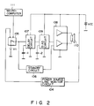
- Fig. 2 is a block diagram showing the principle of a power amplifier according to an embodiment of the present invention.
- Power source line monitor circuit 104 is connected to a power source (Vcc) line and turns on or off standby switch 105 in accordance with variations in a power source voltage.
- Standby switch 105 is turned on or off by signals output from microcomputer 111.
- Reference voltage V1 is applied to standby circuit 106 and delay circuit 107 by means of standby switch 105.
- Standby circuit 106 is connected to amplifier circuit 108.
- Delay circuit 107 is connected to bias circuit 109 serving as a bias source of amplifier circuit 108.
- Bias circuit 109 is connected to amplifier circuit 108 having a BTL structure.
- Load 110 such as a speaker is connected to an output of amplifier circuit 108.
- standby switch 105 When power source line monitor circuit 104 detects that the power source voltage has been dropped by a predetermined value, standby switch 105 is turned off, irrespective of the signals output from microcomputer 111. The instant that standby switch 105 is turned off, standby circuit 106 increases the amplitude of an output voltage of amplifier circuit 108 in the same phase so as to reach a power source voltage or a ground voltage (or negative power source voltage) to extinguish an output waveform of amplifier circuit 108. At the same time, delay circuit 107 is operated to delay the signal by predetermined time by the time constant depending upon capacitance C1 of capacitor 1, and then the bias source of amplifier circuit 108 is cut off.
- delay circuit 107 since delay circuit 107 is connected between standby switch 105 and bias circuit 109, no pop is generated on an output signal when the power source voltage is decreased after a transfer to the standby state.
- the time constant of delay circuit 107 has only to be preset so as to always cut off the bias source before standby circuit 106 for maintaining the standby state is disabled from normally operating.
- Fig. 3 illustrates arrangements of delay circuit 107 and bias circuit 109 of the power amplifier shown in Fig. 2.
- Reference voltage V1 is applied to the bases of npn transistor Q1 and Q2 through standby switch 105.
- the emitters of transistors Q1 and Q2 are connected to ground (GND).
- the collector of transistor Q1 is connected to the base of pnp transistor Q3 through resistor 3.
- the emitter of transistor Q3 is connected to a power source (Vcc) line.
- the collector of transistor Q3 is connected to ground through resistors 4 and 5 and diode-connected transistors Q4 and Q5.
- Capacitor 2 is connected between a ground and a connecting point of resistors 4 and 5 and also connected to the base of npn transistor Q6.
- the collector of transistor Q6 is connected to the power source line.
- the emitter of transistor Q6 is connected to ground through resistor 6 and diode-connected transistors Q7 and Q8.
- the base of npn transistor Q9 is connected between resistor 6 and diode-connected transistors Q7 and Q8.
- the emitter of transistor Q9 is connected to ground through resistor 7.
- the collector of transistor Q9 is connected to the base and collector of pnp transistor Q10.
- the emitter of transistor Q10 is connected to the power source line.
- the base of transistor Q10 is connected to the base of pnp transistor Q11.
- the emitter of transistor Q11 is connected to the power source line.
- the collector of transistor Q11 is connected to the collector of transistor Q2 and the base of npn transistor Q12 and also connected to ground through capacitor 1.
- the emitter of transistor Q12 is grounded.
- the collector of transistor Q12 is connected between resistor 5 and diode-connected transistors Q4 and Q5 and also connected to the base of npn transistor Q13.
- amplifier circuit 108 When amplifier circuit 108 is in an on-state, i.e., when the amplifier circuit generates an output signal, standby switch 105 is closed and reference voltage V1 is applied to transistors Q1 and Q2. Transistors Q1 and Q2 are thus rendered in an on-state and transistor Q3 is turned on. Transistors Q4 to Q11 and Q13 are turned on, accordingly. Transistor Q12 is however cut off since transistor Q2 is turned on. This is because the voltage between the base and emitter of transistor Q12 corresponds to a saturated voltage between the collector and emitter of transistor Q2 and therefore it can be regarded as ⁇ 0.
- Power source line monitor circuit 104 causes an external trigger to turn off standby switch 105 and, in this time, transistors Q1 to Q3 are instantaneously turned off. However, transistors Q4 to Q11 and Q13 are kept in an on-state for a while since the charges of capacitor 2 are maintained by the time constant of about C2 (capacitance of capacitor 2) ⁇ R5 (resistance of resistor 5).
- collector current I CQ11 is expressed by the following equation.
- I CQ11 (V BEQ7 + V BEQ8 - V BEQ9 )/R 7 ⁇ V BE /R 7
- R7 is a resistance of resistor R7
- V BEQ7 , V BEQ8 and V BEQ9 are voltages between the bases and emitters of transistors Q7, Q8 and Q9
- the collector current is thus a constant current.
- collector current I CQ11 is connected to ground through transistor Q2.
- transistor Q2 When transistor Q2 is turned off, capacitor 1 starts to be charged.
- Transistor Q12 can thus be turned on when electric charge q arrives at the time satisfying the following condition.
- Transistor Q12 is thus turned on after a lapse of time t. If transistor Q12 is turned on, transistor Q13 is turned off and accordingly the bias source of the amplifier circuit is cut off.
- delay time t is set so that the bias source can be cut off before a decrease in the power source voltage prevents standby circuit 106 from normally operating, no abnormal sound occurs.
- t ⁇ C 2 ⁇ R 5 ⁇ C 1 ⁇ V BEQ12 (ON) ⁇ /I CQ11 ⁇ C 2 ⁇ R 5
- the bias source cannot be cut off instantaneously but after a lapse of predetermined delay time t after the waveform of an output signal is extinguished by standby circuit 105. An output signal of amplifier circuit 108 can thus be extinguished without any remaining sound or uncomfortable pop. Furthermore, after the bias source of amplifier circuit 108 is cut off and the other bias sources are then cut off, the whole system including the power amplifier is completely turned off. Delay time t is always set shorter than the time in which standby circuit 106 is disabled from normally operating when the power source voltage is decreased after the on-state is changed to the standby state. Even if standby circuit 106 is turned off by the decrease in the power source voltage, the bias source of amplifier circuit 108 is cut off.
- amplifier circuit 108 does not malfunction, nor is any abnormal sound generated from amplifier circuit 108.
- a system for reducing an output voltage and preventing an abnormal sound from generating when an output is cut off can be formed in a power amplifier, an audio system or the like having a standby switch.
Landscapes
- Engineering & Computer Science (AREA)
- Power Engineering (AREA)
- Amplifiers (AREA)
- Bipolar Integrated Circuits (AREA)
Claims (5)
- Amplificateur de puissance comportant un commutateur d'attente (105), comprenant :un circuit d'amplificateur (108) ;un circuit de polarisation (109) jouant le rôle de source de polarisation dudit circuit d'amplificateur ; etun circuit d'attente (106) au moyen duquel deux signaux d'entrée dudit amplificateur de puissance s'annulent l'un l'autre par rapport à la charge de sortie du fait qu'ils sont commandés pour s'approcher de la même valeur au moment où le commutateur d'attente est désactivé, dans lequel ledit circuit d'attente (106) reste pleinement opérationnel pendant une période temporelle prédéterminée dans le cas où la tension de source d'alimentation chute au-dessous du point où l'amplificateur de puissance et le circuit d'attente peuvent encore être normalement activés, et ledit commutateur d'attente (105) coupe ladite source de polarisation (109) vis-à-vis dudit circuit d'amplificateur (108) conformément à des signaux émis en sortie depuis un circuit de commande d'attente (111),
caractérisé en ce que :un circuit de surveillance de ligne d'alimentation en tant que circuit de détecteur (104) surveille la diminution d'une tension de source d'alimentation appliquée sur ledit circuit d'amplificateur et sur ledit circuit de polarisation et lorsque ledit circuit de surveillance de ligne d'alimentation détecte que la tension de source d'alimentation a chuté d'une valeur prédéterminée, ledit commutateur d'attente (105) est désactivé indépendamment des signaux émis en sortie depuis un micro-calculateur (111) en tant que dit circuit de commande d'attente ; etun circuit de retard (107) coupe ladite source de polarisation (109) vis-à-vis dudit circuit d'amplificateur (108) après l'écoulement d'une période temporelle après que le commutateur d'attente (105) est désactivé, ladite période temporelle étant plus courte que ladite période temporelle prédéterminée pendant laquelle l'amplificateur de puissance et le circuit d'attente peuvent encore être normalement activés. - Amplificateur de puissance selon la revendication 1, caractérisé en ce que ledit circuit d'amplificateur (108) comprend un circuit d'amplificateur selon une configuration de pont comportant des première et seconde tensions de sortie.
- Amplificateur de puissance selon l'une quelconque des revendications précédentes, caractérisé en ce que ledit circuit d'attente (106) maximise, du point de vue de la phase, les deux sorties du circuit d'amplificateur (108) selon une configuration de pont pour les amener vers la même valeur, ce qui minimise le signal de sortie.
- Amplificateur de puissance selon l'une quelconque des revendications précédentes, caractérisé en ce que ledit circuit de détecteur (104) commute ledit commutateur d'attente (105) de manière à commuter ledit amplificateur de puissance dans un mode attente lorsque la tension de source d'alimentation chute au-dessous d'une valeur prédéterminée.
- Amplificateur de puissance selon l'une quelconque des revendications précédentes, caractérisé en ce que ledit micro-calculateur (111) commande ledit commutateur d'attente (105) dans un état de fonctionnement normal.
Applications Claiming Priority (2)
| Application Number | Priority Date | Filing Date | Title |
|---|---|---|---|
| JP1311354A JPH0666592B2 (ja) | 1989-11-30 | 1989-11-30 | 電力増幅装置 |
| JP311354/89 | 1989-11-30 |
Publications (3)
| Publication Number | Publication Date |
|---|---|
| EP0430236A2 EP0430236A2 (fr) | 1991-06-05 |
| EP0430236A3 EP0430236A3 (en) | 1991-10-16 |
| EP0430236B1 true EP0430236B1 (fr) | 1996-01-17 |
Family
ID=18016147
Family Applications (1)
| Application Number | Title | Priority Date | Filing Date |
|---|---|---|---|
| EP90122849A Expired - Lifetime EP0430236B1 (fr) | 1989-11-30 | 1990-11-29 | Amplificateur de puissance |
Country Status (5)
| Country | Link |
|---|---|
| US (1) | US5081426A (fr) |
| EP (1) | EP0430236B1 (fr) |
| JP (1) | JPH0666592B2 (fr) |
| KR (1) | KR950003136B1 (fr) |
| DE (1) | DE69024922T2 (fr) |
Families Citing this family (8)
| Publication number | Priority date | Publication date | Assignee | Title |
|---|---|---|---|---|
| AU2471395A (en) * | 1994-05-10 | 1995-11-29 | Apple Computer, Inc. | A method and apparatus for controlling power for subsystems |
| US6366170B1 (en) * | 2000-04-06 | 2002-04-02 | National Semiconductor Corporation | PNP high-current, high-swing output stage and method |
| JP2004336765A (ja) * | 2003-05-02 | 2004-11-25 | Samsung Electronics Co Ltd | ポップノイズ減少のための音声信号発生装置及び音声信号発生方法 |
| TW200722805A (en) * | 2005-12-09 | 2007-06-16 | Ind Tech Res Inst | Canted-fiber base duplex optical subassembly |
| TWI350708B (en) * | 2007-06-26 | 2011-10-11 | Wolo Mfg Corp | Computer controlled amplifier and speaker system with power conservation feature |
| CN101425781B (zh) * | 2007-11-02 | 2011-07-27 | 鸿富锦精密工业(深圳)有限公司 | 音频功率放大装置 |
| KR101288216B1 (ko) | 2011-09-23 | 2013-07-18 | 삼성전기주식회사 | 전력 증폭기 |
| CN105187748B (zh) * | 2015-07-30 | 2019-04-26 | 北京京东方多媒体科技有限公司 | 待机控制电路及显示装置 |
Family Cites Families (10)
| Publication number | Priority date | Publication date | Assignee | Title |
|---|---|---|---|---|
| JPS5651685B2 (fr) * | 1971-11-13 | 1981-12-07 | ||
| JPS5323419Y2 (fr) * | 1972-11-20 | 1978-06-16 | ||
| JPS5517534Y2 (fr) * | 1973-02-02 | 1980-04-23 | ||
| JPS5132246U (fr) * | 1974-08-31 | 1976-03-09 | ||
| US4441086A (en) * | 1982-05-13 | 1984-04-03 | General Motors Corporation | Audio system with orderly shutdown sequence |
| JPS6040114U (ja) * | 1983-08-29 | 1985-03-20 | 三洋電機株式会社 | ショック音防止回路 |
| JPS62186512U (fr) * | 1986-05-16 | 1987-11-27 | ||
| JP2547781B2 (ja) * | 1987-07-13 | 1996-10-23 | 株式会社東芝 | Btl電力増幅回路 |
| IT1217773B (it) * | 1988-06-02 | 1990-03-30 | Sgs Thomson Microelectronics | Circuito di ammutolimento per amplificatori audio |
| IT1229860B (it) * | 1988-11-09 | 1991-09-13 | Sgs Thomson Microelectronics | Amplificatore audio integrato con regolazione unificata delle funzioni di "mute" e "stand by" e dei transitori di commutazione. |
-
1989
- 1989-11-30 JP JP1311354A patent/JPH0666592B2/ja not_active Expired - Lifetime
-
1990
- 1990-11-29 EP EP90122849A patent/EP0430236B1/fr not_active Expired - Lifetime
- 1990-11-29 DE DE69024922T patent/DE69024922T2/de not_active Expired - Fee Related
- 1990-11-30 KR KR1019900019527A patent/KR950003136B1/ko not_active Expired - Lifetime
- 1990-11-30 US US07/619,976 patent/US5081426A/en not_active Expired - Lifetime
Also Published As
| Publication number | Publication date |
|---|---|
| EP0430236A2 (fr) | 1991-06-05 |
| JPH03171766A (ja) | 1991-07-25 |
| US5081426A (en) | 1992-01-14 |
| EP0430236A3 (en) | 1991-10-16 |
| KR910010830A (ko) | 1991-06-29 |
| JPH0666592B2 (ja) | 1994-08-24 |
| DE69024922D1 (de) | 1996-02-29 |
| KR950003136B1 (ko) | 1995-04-01 |
| DE69024922T2 (de) | 1996-06-27 |
Similar Documents
| Publication | Publication Date | Title |
|---|---|---|
| US4301330A (en) | Loudspeaker protection circuit | |
| EP0368528B1 (fr) | Amplificateur audio avec états d'attente et muets | |
| US4887298A (en) | Electronic circuit for sensing disconnect or failure of a power output sense line in an audio power system | |
| WO1997018612A1 (fr) | Systeme de distribution de puissance insensible aux defaillances | |
| EP0430236B1 (fr) | Amplificateur de puissance | |
| KR100251837B1 (ko) | 오디오 출력 채널용 보호 장치 | |
| US5914586A (en) | Power supply | |
| US5357395A (en) | Undervoltage protection circuit, system and method of operating same | |
| KR960006488A (ko) | 고속동작 제어 시스템 | |
| US4481553A (en) | Protection circuit | |
| US3990019A (en) | Power amplifier having protective circuits | |
| US4184187A (en) | Unbalanced DC voltage detecting circuit | |
| JP3838708B2 (ja) | リチウムイオン電源装置 | |
| JPH08321756A (ja) | 半導体素子駆動回路 | |
| US3860855A (en) | Multiple voltage source imbalance detection and protection circuit | |
| JPH0225284B2 (fr) | ||
| JPS6339162B2 (fr) | ||
| JPH05257502A (ja) | オン/オフされる電子機器中の装置 | |
| KR900010614Y1 (ko) | 오디오 파워 앰프의 과 입력보호 회로 | |
| US4435844A (en) | Remote control circuit | |
| KR860001128Y1 (ko) | 파워앰프와 스피이커 보호회로 | |
| JP2729057B2 (ja) | 電力増幅装置 | |
| JP2790471B2 (ja) | ミューティング回路 | |
| US3930207A (en) | Amplifier with overload protection | |
| JPH062372Y2 (ja) | Agc回路 |
Legal Events
| Date | Code | Title | Description |
|---|---|---|---|
| PUAI | Public reference made under article 153(3) epc to a published international application that has entered the european phase |
Free format text: ORIGINAL CODE: 0009012 |
|
| 17P | Request for examination filed |
Effective date: 19901129 |
|
| AK | Designated contracting states |
Kind code of ref document: A2 Designated state(s): DE FR GB |
|
| PUAL | Search report despatched |
Free format text: ORIGINAL CODE: 0009013 |
|
| AK | Designated contracting states |
Kind code of ref document: A3 Designated state(s): DE FR GB |
|
| 17Q | First examination report despatched |
Effective date: 19940421 |
|
| GRAA | (expected) grant |
Free format text: ORIGINAL CODE: 0009210 |
|
| AK | Designated contracting states |
Kind code of ref document: B1 Designated state(s): DE FR GB |
|
| REF | Corresponds to: |
Ref document number: 69024922 Country of ref document: DE Date of ref document: 19960229 |
|
| ET | Fr: translation filed | ||
| PLBE | No opposition filed within time limit |
Free format text: ORIGINAL CODE: 0009261 |
|
| STAA | Information on the status of an ep patent application or granted ep patent |
Free format text: STATUS: NO OPPOSITION FILED WITHIN TIME LIMIT |
|
| 26N | No opposition filed | ||
| PGFP | Annual fee paid to national office [announced via postgrant information from national office to epo] |
Ref country code: FR Payment date: 19971112 Year of fee payment: 8 |
|
| PGFP | Annual fee paid to national office [announced via postgrant information from national office to epo] |
Ref country code: GB Payment date: 19971120 Year of fee payment: 8 |
|
| PG25 | Lapsed in a contracting state [announced via postgrant information from national office to epo] |
Ref country code: GB Free format text: LAPSE BECAUSE OF NON-PAYMENT OF DUE FEES Effective date: 19981129 |
|
| GBPC | Gb: european patent ceased through non-payment of renewal fee |
Effective date: 19981129 |
|
| PG25 | Lapsed in a contracting state [announced via postgrant information from national office to epo] |
Ref country code: FR Free format text: LAPSE BECAUSE OF NON-PAYMENT OF DUE FEES Effective date: 19990730 |
|
| REG | Reference to a national code |
Ref country code: FR Ref legal event code: ST |
|
| PGFP | Annual fee paid to national office [announced via postgrant information from national office to epo] |
Ref country code: DE Payment date: 20071122 Year of fee payment: 18 |
|
| PG25 | Lapsed in a contracting state [announced via postgrant information from national office to epo] |
Ref country code: DE Free format text: LAPSE BECAUSE OF NON-PAYMENT OF DUE FEES Effective date: 20090603 |