EP0430653A2 - Circuit ECL avec diodes de charge - Google Patents
Circuit ECL avec diodes de charge Download PDFInfo
- Publication number
- EP0430653A2 EP0430653A2 EP90312897A EP90312897A EP0430653A2 EP 0430653 A2 EP0430653 A2 EP 0430653A2 EP 90312897 A EP90312897 A EP 90312897A EP 90312897 A EP90312897 A EP 90312897A EP 0430653 A2 EP0430653 A2 EP 0430653A2
- Authority
- EP
- European Patent Office
- Prior art keywords
- coupled
- transistor
- diode
- current
- emitter
- Prior art date
- Legal status (The legal status is an assumption and is not a legal conclusion. Google has not performed a legal analysis and makes no representation as to the accuracy of the status listed.)
- Granted
Links
Images
Classifications
-
- H—ELECTRICITY
- H03—ELECTRONIC CIRCUITRY
- H03K—PULSE TECHNIQUE
- H03K19/00—Logic circuits, i.e. having at least two inputs acting on one output; Inverting circuits
- H03K19/02—Logic circuits, i.e. having at least two inputs acting on one output; Inverting circuits using specified components
- H03K19/08—Logic circuits, i.e. having at least two inputs acting on one output; Inverting circuits using specified components using semiconductor devices
- H03K19/082—Logic circuits, i.e. having at least two inputs acting on one output; Inverting circuits using specified components using semiconductor devices using bipolar transistors
- H03K19/086—Emitter coupled logic
-
- G—PHYSICS
- G05—CONTROLLING; REGULATING
- G05F—SYSTEMS FOR REGULATING ELECTRIC OR MAGNETIC VARIABLES
- G05F3/00—Non-retroactive systems for regulating electric variables by using an uncontrolled element, or an uncontrolled combination of elements, such element or such combination having self-regulating properties
- G05F3/02—Regulating voltage or current
- G05F3/08—Regulating voltage or current wherein the variable is DC
- G05F3/10—Regulating voltage or current wherein the variable is DC using uncontrolled devices with non-linear characteristics
- G05F3/16—Regulating voltage or current wherein the variable is DC using uncontrolled devices with non-linear characteristics being semiconductor devices
- G05F3/20—Regulating voltage or current wherein the variable is DC using uncontrolled devices with non-linear characteristics being semiconductor devices using diode- transistor combinations
- G05F3/22—Regulating voltage or current wherein the variable is DC using uncontrolled devices with non-linear characteristics being semiconductor devices using diode- transistor combinations wherein the transistors are of the bipolar type only
Definitions
- the present invention relates to emitter coupled logic and current mode logic circuits and, more particularly, to diode load emitter coupled logic circuits (DLECL).
- DLECL diode load emitter coupled logic circuits
- DLECL circuits are known in the art which use diodes as the load elements of the emitter coupled logic circuit to provide a minimum logic output voltage swing to thereby increase the operation speed of the logic circuit.
- DLECL circuits are operated differentially, i.e., the input logic signals are differentially applied to the emitter coupled input stage of the logic circuit.
- feedback counters are generally constructed with flip-flops connected in series with one or more outputs that are fed back to the first flip-flop of the counter through a DLECL gate. These outputs to the gate are differentially coupled thereto.
- Another example of a differentially coupled DLECL circuit is a modulus divider described in U.S. Patent No. 4,585,957.
- a common problem with operating DLECL circuits differentially is that this requires series gating, i.e., the stacking of ECL gates to obtain the necessary logic function.
- series gating may conserve current requirement it requires at least an additional diode voltage drop between the power supply which thus limits the minimum supply voltage and also requires the driving output to be level shifted which is usually accomplished using emitter followers which use additional current.
- a solution or alternative method is to use a single-ended logic input to the DLECL instead of differential applied logic input. This however requires a reference or threshold voltage that is applied to one input of the gate in order to have the gate logically switch output operating states in response to the logic input varying above and below the reference voltage. This reference voltage must ideally be centered between the logic output signal swing.
- Still another aspect of the present invention is to provide a voltage reference generator for use in a single-ended operated DLECL circuit.
- a voltage generator for providing a reference potential at an output which includes a first transistor the emitter of which is coupled to the output and a collector that is coupled to a first power supply conductor, a diode is coupled between the first power supply conductor and the base of the first transistor while a current supply is coupled between the emitter of the first transistor and a second power supply conductor.
- the voltage generator is utilized in a single-ended DLECL circuit wherein the output of the generator is connected to a first input of the DLECL circuit while the second input thereof receives a single-ended logic input signal.
- the current supply supplies a current the magnitude of which is substantially equal to the common current supply of the DLECL circuit.
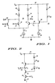
- Fig. 1 is a schematic diagram illustrating a single-ended DLECL circuit of the present invention which includes a threshold voltage generator circuit of a preferred embodiment
- Fig. 2 is a schematic diagram of a of threshold voltage generator of a second embodiment of the present invention.
- Fig. 1 there is shown single-ended operated DLECL circuit 10 of the present invention including the novel threshold voltage generator circuit 42 of the present invention.
- DLECL circuit is shown as a simple OR/NOR gate; it being understood that other DLECL circuits having other logic functions and operated single-ended can utilize threshold voltage generator 42 in a similar manner to be described herein.
- the OR/NOR gate includes emitter-coupled transistors 12, 14 and 16 with the bases of transistors 12 and 16 receiving logic input signals supplied thereto at inputs 18 and 20.
- the interconnected emitters are coupled to current supply 22 which is returned to power supply conductor 24 to which is supplied ground reference potential.
- Diode load circuitry 26 including diodes 28 and 30 series coupled between the collectors of transistors 12 and 16 and power supply conductor 36 as well as diodes 32 and 34 series coupled between the collector of transistor 14 and power supply conductor 36, provides a minimum logic output signal swing at the Q output, terminal 38, and at the Q output, terminal 39, of DLECL circuit 10.
- DLECL circuit 10 In order to operate DLECL circuit 10 in a single-ended mode it is necessary that the base of transistor 14 be supplied a threshold reference potential V T that is substantially equal to one-half the logic input signal swing applied to inputs INA and INB (inputs 18 and 20).
- the logic input signals are supplied from a previous DLECL circuit wherein the logic swing is derived across a pair of diode loads similar to diodes 28 and 30.
- the outputs of DLECL circuit 10 will usually be supplied to inputs of a similar logic circuit or to emitter followers.
- the Q output terminal 38
- the Q output terminal 38
- DLECL circuit 10 when INA is greater than V T , transistor 12 is turned on and transistor 14 is turned off such that I T flows through the transistor and diodes 28 and 30 as transistors 12, 14 and 16 are operated in a non-saturating mode as understood. Conversely, as inputs INA and INB are less than V T , transistor 12 tends to be turned off where the current I T flows through transistor 14 and diodes 32 and 34.
- the only current flowing through diodes 28 and 30 is base current required by the emitter follower or next logic circuit coupled to output 38 which, assuming the following circuit is biased by a current I T , will be equal to I T / ⁇ , where ⁇ is the forward current gain of the following circuit having a transistor with its base coupled to output 38 and operated in a non-saturating mode.
- the voltage swing across diode loads 28 and 30 can be determined by comparing the voltage at output 38 as the logic signal thereat is switched between high, V H , and low, V L , output states.
- the present invention now proceeds to realize a voltage threshold generator that will supply the value of V T stated in equation 5.
- FIG. 1 there is illustrated voltage threshold generator 42 for providing the required V T necessary to permit single-ended operation of DLECL circuit 10.
- Generator 42 is shown as comprising transistor 44 the emitter of which is coupled to terminal 40 at which the threshold voltage V T is provided.
- the collector of transistor 44 is coupled to power supply conductor 36 while diode 46 is connected between the power supply conductor and the base of the transistor.
- Current supply 48 which sinks a current I T through transistor 44 is coupled between the emitter thereof and power supply conductor 24.
- terminal 38 may in some circuit configurations such as feedback counters not only be coupled to the base of a transistor of a next DLECL circuit but may also be coupled to another input whereby in the high state two factors of I T / ⁇ flow through the diode loads.
- the second term of equation 5 would be equal to (kT/q) In (2 I T ⁇ /I s ).
- V T Vcc-(kT/q) In (2 I T ⁇ /I s )-(kT/q) In ( I T I s ).
- Threshold voltage generator circuit 50 is shown as including an additional transistor 52 the collector-emitter conduction path of which is coupled between the emitter of transistor 44 and current supply 48.
- Current supply 48 as illustrated may be comprised of a transistor 54 that has its base biased to a potential V B in order to sink the current I T .
- An additional diode 56 is coupled between the base of transistor 44 and the base of transistor 52 the latter of which is also operated in a non-saturated state. It is understood that all diodes may be realized by an NPN transistor having its base and collector shorted together to form the anode of the diode while the emitter forms the cathode of the diode. Therefore, since transistor 44 and diode 46 can be identical to the diode loads, the magnitude of V T will track and remain midway between the voltage swing across the diode loads over process variations, temperature and ⁇ variations.
- novel voltage threshold generators for providing a threshold voltage for biasing a single-ended operated DLECL circuit.
- the threshold voltage has a magnitude that tracks the non-linear diode loads of the DLECL circuit and is substantially equal to a value that lies midway between the logic signal output swing developed across the diode loads.
Landscapes
- Engineering & Computer Science (AREA)
- Physics & Mathematics (AREA)
- Microelectronics & Electronic Packaging (AREA)
- Radar, Positioning & Navigation (AREA)
- Electromagnetism (AREA)
- General Physics & Mathematics (AREA)
- Nonlinear Science (AREA)
- Automation & Control Theory (AREA)
- Power Engineering (AREA)
- Computer Hardware Design (AREA)
- Computing Systems (AREA)
- General Engineering & Computer Science (AREA)
- Mathematical Physics (AREA)
- Logic Circuits (AREA)
Applications Claiming Priority (2)
| Application Number | Priority Date | Filing Date | Title |
|---|---|---|---|
| US443790 | 1989-11-30 | ||
| US07/443,790 US5059826A (en) | 1989-11-30 | 1989-11-30 | Voltage threshold generator for use in diode load emitter coupled logic circuits |
Publications (3)
| Publication Number | Publication Date |
|---|---|
| EP0430653A2 true EP0430653A2 (fr) | 1991-06-05 |
| EP0430653A3 EP0430653A3 (en) | 1991-07-24 |
| EP0430653B1 EP0430653B1 (fr) | 1995-08-30 |
Family
ID=23762218
Family Applications (1)
| Application Number | Title | Priority Date | Filing Date |
|---|---|---|---|
| EP90312897A Expired - Lifetime EP0430653B1 (fr) | 1989-11-30 | 1990-11-27 | Circuit ECL avec diodes de charge |
Country Status (4)
| Country | Link |
|---|---|
| US (1) | US5059826A (fr) |
| EP (1) | EP0430653B1 (fr) |
| JP (1) | JPH03186014A (fr) |
| DE (1) | DE69022001T2 (fr) |
Cited By (2)
| Publication number | Priority date | Publication date | Assignee | Title |
|---|---|---|---|---|
| EP0476341A1 (fr) * | 1990-08-29 | 1992-03-25 | Motorola, Inc. | Circuit logique BICMOS avec une sortie CML |
| EP0651512A3 (fr) * | 1993-11-03 | 1995-12-06 | Siemens Ag | Etage inverseur. |
Families Citing this family (1)
| Publication number | Priority date | Publication date | Assignee | Title |
|---|---|---|---|---|
| US8373318B2 (en) | 2010-04-30 | 2013-02-12 | Hamilton Sundstrand Corporation | Terminal lead insulator assembly for wound field synchronous machine |
Family Cites Families (4)
| Publication number | Priority date | Publication date | Assignee | Title |
|---|---|---|---|---|
| FR2534752A1 (fr) * | 1982-10-18 | 1984-04-20 | Radiotechnique Compelec | Circuit convertisseur de niveaux de signaux entre une logique de type saturee et une logique de type non saturee |
| US4585957A (en) * | 1983-04-25 | 1986-04-29 | Motorola Inc. | Diode load emitter coupled logic circuits |
| JPH0638217B2 (ja) * | 1985-11-30 | 1994-05-18 | 株式会社東芝 | 熱保護回路 |
| US4806796A (en) * | 1988-03-28 | 1989-02-21 | Motorola, Inc. | Active load for emitter coupled logic gate |
-
1989
- 1989-11-30 US US07/443,790 patent/US5059826A/en not_active Expired - Lifetime
-
1990
- 1990-11-27 EP EP90312897A patent/EP0430653B1/fr not_active Expired - Lifetime
- 1990-11-27 DE DE69022001T patent/DE69022001T2/de not_active Expired - Fee Related
- 1990-11-29 JP JP2326078A patent/JPH03186014A/ja active Pending
Cited By (3)
| Publication number | Priority date | Publication date | Assignee | Title |
|---|---|---|---|---|
| EP0476341A1 (fr) * | 1990-08-29 | 1992-03-25 | Motorola, Inc. | Circuit logique BICMOS avec une sortie CML |
| EP0651512A3 (fr) * | 1993-11-03 | 1995-12-06 | Siemens Ag | Etage inverseur. |
| US5521558A (en) * | 1993-11-03 | 1996-05-28 | Siemens Aktiengesellschaft | Inverter stage having diode load and ring oscillator using same |
Also Published As
| Publication number | Publication date |
|---|---|
| DE69022001D1 (de) | 1995-10-05 |
| DE69022001T2 (de) | 1996-05-02 |
| EP0430653B1 (fr) | 1995-08-30 |
| US5059826A (en) | 1991-10-22 |
| EP0430653A3 (en) | 1991-07-24 |
| JPH03186014A (ja) | 1991-08-14 |
Similar Documents
| Publication | Publication Date | Title |
|---|---|---|
| US5079452A (en) | High speed ECL latch with clock enable | |
| US4518876A (en) | TTL-ECL Input translation with AND/NAND function | |
| JPH03149920A (ja) | 電圧変換器 | |
| US4435654A (en) | Output level adjustment means for low fanout ECL lacking emitter follower output | |
| US5815019A (en) | Flip-flop circuit operating on low voltage | |
| US4728821A (en) | Source follower current mode logic cells | |
| EP0111262A2 (fr) | Multiplexeur de sortie avec un retard équivalent à celui d'une porte | |
| EP0183464B1 (fr) | Circuits logiques à émetteurs couplés | |
| EP0430653B1 (fr) | Circuit ECL avec diodes de charge | |
| US4945263A (en) | TTL to ECL/CML translator circuit with differential output | |
| US4717839A (en) | Transistor comparator circuit having split collector feedback hysteresis | |
| US5631580A (en) | BICMOS ECL-CMOS level converter | |
| US4529894A (en) | Means for enhancing logic circuit performance | |
| US4928024A (en) | Referenceless ECL logic circuit | |
| JPH0738414A (ja) | シングルエンド入力論理ゲートを有する集積論理回路 | |
| US5039881A (en) | High speed, low power input buffer | |
| US4845387A (en) | Non-stacked ECL type and function | |
| EP0406609A2 (fr) | Translateur ECL/TTL à deux tensions d'alimentation | |
| US4734656A (en) | Merged integrated oscillator circuit | |
| US4871929A (en) | ECL logic gate | |
| US4259599A (en) | Complementary transistor switching circuit | |
| US4782248A (en) | STL exclusive-or buffer | |
| EP0147635A2 (fr) | Porte ayant une capacité de miller réduite | |
| US4954738A (en) | Current source technology | |
| KR920008047B1 (ko) | 논리회로 |
Legal Events
| Date | Code | Title | Description |
|---|---|---|---|
| PUAI | Public reference made under article 153(3) epc to a published international application that has entered the european phase |
Free format text: ORIGINAL CODE: 0009012 |
|
| AK | Designated contracting states |
Kind code of ref document: A2 Designated state(s): DE FR GB IT |
|
| PUAL | Search report despatched |
Free format text: ORIGINAL CODE: 0009013 |
|
| AK | Designated contracting states |
Kind code of ref document: A3 Designated state(s): DE FR GB IT |
|
| 17P | Request for examination filed |
Effective date: 19910823 |
|
| 17Q | First examination report despatched |
Effective date: 19940221 |
|
| GRAA | (expected) grant |
Free format text: ORIGINAL CODE: 0009210 |
|
| AK | Designated contracting states |
Kind code of ref document: B1 Designated state(s): DE FR GB IT |
|
| ITF | It: translation for a ep patent filed | ||
| REF | Corresponds to: |
Ref document number: 69022001 Country of ref document: DE Date of ref document: 19951005 |
|
| ET | Fr: translation filed | ||
| PLBE | No opposition filed within time limit |
Free format text: ORIGINAL CODE: 0009261 |
|
| STAA | Information on the status of an ep patent application or granted ep patent |
Free format text: STATUS: NO OPPOSITION FILED WITHIN TIME LIMIT |
|
| 26N | No opposition filed | ||
| PGFP | Annual fee paid to national office [announced via postgrant information from national office to epo] |
Ref country code: FR Payment date: 19971015 Year of fee payment: 8 |
|
| PGFP | Annual fee paid to national office [announced via postgrant information from national office to epo] |
Ref country code: DE Payment date: 19971023 Year of fee payment: 8 |
|
| PGFP | Annual fee paid to national office [announced via postgrant information from national office to epo] |
Ref country code: GB Payment date: 19981001 Year of fee payment: 9 |
|
| PG25 | Lapsed in a contracting state [announced via postgrant information from national office to epo] |
Ref country code: FR Free format text: LAPSE BECAUSE OF NON-PAYMENT OF DUE FEES Effective date: 19990730 |
|
| REG | Reference to a national code |
Ref country code: FR Ref legal event code: ST |
|
| PG25 | Lapsed in a contracting state [announced via postgrant information from national office to epo] |
Ref country code: DE Free format text: LAPSE BECAUSE OF NON-PAYMENT OF DUE FEES Effective date: 19990901 |
|
| PG25 | Lapsed in a contracting state [announced via postgrant information from national office to epo] |
Ref country code: GB Free format text: LAPSE BECAUSE OF NON-PAYMENT OF DUE FEES Effective date: 19991127 |
|
| GBPC | Gb: european patent ceased through non-payment of renewal fee |
Effective date: 19991127 |
|
| PG25 | Lapsed in a contracting state [announced via postgrant information from national office to epo] |
Ref country code: IT Free format text: LAPSE BECAUSE OF NON-PAYMENT OF DUE FEES Effective date: 20051127 |