EP0431435B1 - Automatische Verstärkungsregelung in einem Demodulator eines digitalen Empfängers - Google Patents
Automatische Verstärkungsregelung in einem Demodulator eines digitalen Empfängers Download PDFInfo
- Publication number
- EP0431435B1 EP0431435B1 EP19900122516 EP90122516A EP0431435B1 EP 0431435 B1 EP0431435 B1 EP 0431435B1 EP 19900122516 EP19900122516 EP 19900122516 EP 90122516 A EP90122516 A EP 90122516A EP 0431435 B1 EP0431435 B1 EP 0431435B1
- Authority
- EP
- European Patent Office
- Prior art keywords
- digital
- demodulator
- agc
- input
- signal
- Prior art date
- Legal status (The legal status is an assumption and is not a legal conclusion. Google has not performed a legal analysis and makes no representation as to the accuracy of the status listed.)
- Expired - Lifetime
Links
Images
Classifications
-
- H—ELECTRICITY
- H03—ELECTRONIC CIRCUITRY
- H03G—CONTROL OF AMPLIFICATION
- H03G3/00—Gain control in amplifiers or frequency changers
- H03G3/20—Automatic control
- H03G3/30—Automatic control in amplifiers having semiconductor devices
- H03G3/3089—Control of digital or coded signals
Definitions
- the present invention relates to an automatic gain control device for a demodulator fitted to a receiver for a digital information transmission installation.
- AGC Automatic Gain Control
- a first AGC device is provided in the Intermediate Frequency chain, where it provides high dynamics
- a second AGC device is provided at the input of the demodulator, where it provides additional correction of small dynamics, useful for case where a jammer would slip between the templates of the agile reception filter and the narrow filter (generally constituted by a surface wave filter) placed at the input of the demodulator: it is this second AGC device which is concerned by the present invention.
- the AGC device which is placed directly at the input of the demodulator operates as follows:
- the demodulated signal which is obtained on one of the channels, or "eye" is amplified, then applied to a detector followed by a filter, in order to extract therefrom the continuous component representing the amplitude A of the demodulated signal.
- This filtered signal is, if necessary, inverted, then it is applied to the control input of an adjustable attenuator (generally constituted by a PIN diode attenuator) which is located in Intermediate Frequency just before the demodulator.
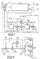
- the reference 1 designates the demodulator of a receiver for a digital transmission installation by radio beam using a modulation of MAQ2 n type, and in this specific example a modulation MAQ4, therefore with four phase states .
- the demodulated signals X and Y, or "eyes" appear respectively on the two output channels 2 and 3 of the demodulator 1.
- an adjustable analog attenuator is placed at the input of the demodulator 1, in series with the incident signal at 5, and it sees its attenuation control input 6 connected to the output of a regulation circuit, of which the input 7 is constituted by the demodulated signal taken on one of the "eyes" and in this example on the eye Y, and which will be described now.
- the signal demodulated on the eye Y whose absolute amplitude will be designated hereinafter by A, is applied to the input 8 of an Analog-Digital converter 9 which is sampled at 10 at the rate of the clock-bit H.
- the sampled digital values which are thus extracted therefrom at 11 are passed through a logic circuit 12 capable of calculating the absolute value of each of these successive samples.
- the signals at 16 are applied to a Digital-Analog converter 17, sampled at the H / 2 rhythm in order to take into account in pairs the aforementioned successive samples (H being the clock-bit).
- the analog signal that leaves at 18 is applied to a smoothing filter (low-pass filter) 19 capable of achieving valid integration on at least several dozen successive signals: it outputs 20 at an analog signal of substantially equal amplitude at 3A / 2, and inverted by an inverter included in the filter 19 (which is for example achieved by the conventional use of an operational amplifier for this filter), and it is this signal which is applied to the input control 6 of the attenuator 4 in order to carry out the desired Automatic Gain Control.
- FIG. 2 An interesting alternative embodiment of the block 21, surrounded by dashed lines in FIG. 1, is shown in FIG. 2.
- This circuit 22 very simply comprises a multiplier 24 receiving the coefficient a and the input signal, followed by a summator 25 which also receives its own output 23 passed through a flip-flop "D" 26 sampled at the rate H / 2, half of that of the clock-bit H.
- the digital signals thus calculated at 23 are output in parallel at 27, so that their constituent bits, from the least significant bit to the most significant bit, are respectively applied to the activation or no control inputs.
- -activation Co, ... .Cn-2, Cn-1, Cn of a cascade 28 of Io attenuators,. ..In-2, In-1, In, which are controllable by all-or-nothing on these respective control inputs Co to Cn, and whose attenuations vary, from Io to In, like the successive binary weights of the bits which their are respectively associated.
- the purpose of the following calculation is to demonstrate the independence of operation of the device of the invention from the sampling instant, and the quality of its linearity.
- the eye transitions are approximated by a sinusoid arc.
- Vp2 ( ⁇ ) A.
- Vp 1, -3 ( ⁇ ) + Vp -1.3 ( ⁇ ) A / 3 + 2A / 3. (
- ) Vp 3.1 ( ⁇ ) + Vp -3, -1 ( ⁇ ) 2A / 3 + A / 3.
- V hardly varies as a function of ⁇ , so that the sampling device used can be simple, even rustic.
Landscapes
- Control Of Amplification And Gain Control (AREA)
- Digital Transmission Methods That Use Modulated Carrier Waves (AREA)
- Cable Transmission Systems, Equalization Of Radio And Reduction Of Echo (AREA)
Claims (4)
- Vorrichtung zur automatischen Verstärkungssteuerung (AGC), die am Eingang des Demodulators (1) eines Empfängers einer digitalen Datenübertragungsanlage liegen soll, dadurch gekennzeichnet, daß die Vorrichtung enthält. erste Mittel (9), die das auf einem der Ausgangskanäle (3) des Demodulators (1) erhaltene und demodulierte Analogsignal in ein im Rhythmus des Bittakts (H) des vom Empfänger empfangenen digitalen Signals getastetes digitales Signal umwandeln,. zweite Mittel (12, 13, 14), die dann jedesmal die Absolutwerte der digitalen Signale betreffend zwei aufeinanderfolgende Tastproben addieren,. dritte Mittel (17 bis 19, 22 bis 27), um dann den Mittelwert (3A/2) über mindestens mehrere zig aufeinanderfolgende Additionen des für jede dieser Additionen erhaltenen Ergebnisses (A oder 2A) zu bestimmen und um diesen Mittelwert (3A/2) zur Steuerung einer regelbaren Spannungs-Dämpfungsvorrichtung (28) zu verwenden, die am Eingang des Demodulators (1) vorgesehen ist.
- AGC-Vorrichtung nach Anspruch 1, dadurch gekennzeichnet, daß die dritten Mittel einen Digital-Analog-Wandler (17) und ein Glättungsfilter (19) enthalten.
- AGC-Vorrichtung nach Anspruch 1, dadurch gekennzeichnet, daß diese dritten Mittel einen digitalen Multiplizier-Akkumulator (22) und eine Kaskade (28) von durch die jeweiligen Bits jedes digitalen Signals am Ausgang des Multiplizier-Akkumulators (22) binär gesteuerten Dämpfungsglieder aufweisen.
- AGC-Vorrichtung nach Anspruch 1, dadurch gekennzeichnet, daß die Dämpfungswirkungen der Dämpfungsglieder der Kaskade (28) wie die jeweiligen binären Gewichte (von Io bis In) der ihnen zugeordneten Bits variieren.
Applications Claiming Priority (2)
| Application Number | Priority Date | Filing Date | Title |
|---|---|---|---|
| FR8915806 | 1989-11-30 | ||
| FR8915806A FR2655217B1 (fr) | 1989-11-30 | 1989-11-30 | Dispositif de commande automatique de gain pour demodulateur equipant un recepteur pour installation de transmission numerique d'informations. |
Publications (2)
| Publication Number | Publication Date |
|---|---|
| EP0431435A1 EP0431435A1 (de) | 1991-06-12 |
| EP0431435B1 true EP0431435B1 (de) | 1995-03-15 |
Family
ID=9387983
Family Applications (1)
| Application Number | Title | Priority Date | Filing Date |
|---|---|---|---|
| EP19900122516 Expired - Lifetime EP0431435B1 (de) | 1989-11-30 | 1990-11-26 | Automatische Verstärkungsregelung in einem Demodulator eines digitalen Empfängers |
Country Status (4)
| Country | Link |
|---|---|
| EP (1) | EP0431435B1 (de) |
| DE (1) | DE69017850T2 (de) |
| ES (1) | ES2070977T3 (de) |
| FR (1) | FR2655217B1 (de) |
Families Citing this family (3)
| Publication number | Priority date | Publication date | Assignee | Title |
|---|---|---|---|---|
| JPH06244889A (ja) * | 1993-02-15 | 1994-09-02 | Fujitsu Ltd | モデム復調部用受信レベル調整回路 |
| DE4327541A1 (de) * | 1993-08-16 | 1995-02-23 | Aeg Mobile Communication | Verfahren zur automatischen Verstärkungsregelung in einem Empfänger |
| EP0702453B1 (de) * | 1994-09-13 | 2001-12-05 | Koninklijke Philips Electronics N.V. | Schaltung zur automatischen Verstärkungsregelung und Vorrichtung mit einer solchen Schaltung |
Family Cites Families (3)
| Publication number | Priority date | Publication date | Assignee | Title |
|---|---|---|---|---|
| IT1121030B (it) * | 1979-09-18 | 1986-03-26 | Cselt Centro Studi Lab Telecom | Procedimento e circuito per il controllo automatico del guadagno in apparecchiature elettroniche |
| JPS57138208A (en) * | 1981-02-20 | 1982-08-26 | Hitachi Ltd | Power detecting circuit and gain control circuit using it |
| EP0213224B1 (de) * | 1985-08-28 | 1990-04-11 | International Business Machines Corporation | Verfahren zur schnellen Verstärkungseinstellung in einem Modemempfänger |
-
1989
- 1989-11-30 FR FR8915806A patent/FR2655217B1/fr not_active Expired - Lifetime
-
1990
- 1990-11-26 EP EP19900122516 patent/EP0431435B1/de not_active Expired - Lifetime
- 1990-11-26 DE DE1990617850 patent/DE69017850T2/de not_active Expired - Fee Related
- 1990-11-26 ES ES90122516T patent/ES2070977T3/es not_active Expired - Lifetime
Also Published As
| Publication number | Publication date |
|---|---|
| DE69017850T2 (de) | 1995-07-06 |
| FR2655217A1 (fr) | 1991-05-31 |
| ES2070977T3 (es) | 1995-06-16 |
| FR2655217B1 (fr) | 1992-02-07 |
| EP0431435A1 (de) | 1991-06-12 |
| DE69017850D1 (de) | 1995-04-20 |
Similar Documents
| Publication | Publication Date | Title |
|---|---|---|
| EP0054829B1 (de) | Verfahren und Einrichtung zur Detektion der Trainingsfolge eines autoadaptiven Entzerrers | |
| FR2598872A1 (fr) | Systeme de demodulation de signal numerique | |
| EP0036084A1 (de) | Verfahren und Vorrichtung zum Steuern der Beginneinstellung des Taktgebers eines Empfängers für synchrone Daten | |
| EP0421897B1 (de) | Vorrichtung zum Extrahieren von digitalen Daten aus einem Video-Signal | |
| EP0013343A1 (de) | Verfahren und Vorrichtung zur Auffindung einer Pseudo-Zufallsfolge von 0 Grad- und 180 Grad-Phasenänderungen der Trägerwelle in einem Datenempfänger | |
| EP0459968B1 (de) | Digitaler Demodulator für mehrphasenmodulierte Signale | |
| EP0679001A1 (de) | Entscheidungseinrichtung mit adaptiven Pegeln für nicht-lineare Modulation | |
| EP0230900B1 (de) | Taktwiedergewinnungseinrichtung | |
| FR2736231A1 (fr) | Systeme de communication numerique comportant un recepteur dote d'un dispositif de recuperation de rythme | |
| EP0431435B1 (de) | Automatische Verstärkungsregelung in einem Demodulator eines digitalen Empfängers | |
| EP0604295B1 (de) | Verfahren zur Verstärkungsregelung in einem digitalen Empfänger, insbesondere einem TDMA-Empfänger und Vorrichtung zur Durchführung des Verfahrens | |
| EP0497250A1 (de) | Verfahren zur Erkennung eines Störsignal für einen digitalen Datendemodulator, und Einrichtung zur Durchführung eines solchen Verfahrens | |
| EP0094040B1 (de) | System zur synchronen Datenübertragung mit Hilfe eines amplitudenmodulierten Trägers konstanter Hüllkurve | |
| CA2144670C (fr) | Dispositif numerique de recuperation large bande d'une porteuse | |
| EP0121750B1 (de) | Taktrückgewinnungschaltung für eine eine Kombination des Biphase-L und des modifizierten Biphase-Kodes verwendende synchrone Datenübertragung | |
| EP0494003B1 (de) | Empfangsanordnung zur Verarbeitung von auf verschiedenen Wegen empfangenen Signalen | |
| EP0329049B1 (de) | Verfahren zur Regelung der Abtastzeitpunkte in einer digitalen Übertragung mit Quadraturträgermodulation und Einrichtung zur Durchführung des Verfahrens | |
| EP0368417B1 (de) | Anordnung mit einer verbesserten Gleichstrompegelauswertungsvorrichtung | |
| WO2003001689A2 (fr) | Systeme d'amplification d'un signal hertzien et decodeur de signaux de television comportant un tel systeme | |
| EP0905946A1 (de) | Reglung der Abtastung von Biphasensignale | |
| EP1246421B1 (de) | FM-Empfänger mit numerischem Demodulator | |
| FR2675001A1 (fr) | Procede et dispositif de modulation numerique a composantes en phase et en quadrature et installation de transmission en comportant application. | |
| FR2720575A1 (fr) | Adaptateur post-démodulation. | |
| EP1261182B1 (de) | Empfänger für frequenzmodulierte Signale mit digitalen Demodulator | |
| FR2551937A1 (fr) | Recepteur radio-electrique a glissement de frequence |
Legal Events
| Date | Code | Title | Description |
|---|---|---|---|
| PUAI | Public reference made under article 153(3) epc to a published international application that has entered the european phase |
Free format text: ORIGINAL CODE: 0009012 |
|
| AK | Designated contracting states |
Kind code of ref document: A1 Designated state(s): DE ES FR GB IT NL SE |
|
| RAP1 | Party data changed (applicant data changed or rights of an application transferred) |
Owner name: ALCATEL TELSPACE |
|
| 17P | Request for examination filed |
Effective date: 19911202 |
|
| 17Q | First examination report despatched |
Effective date: 19940513 |
|
| GRAA | (expected) grant |
Free format text: ORIGINAL CODE: 0009210 |
|
| AK | Designated contracting states |
Kind code of ref document: B1 Designated state(s): DE ES FR GB IT NL SE |
|
| REF | Corresponds to: |
Ref document number: 69017850 Country of ref document: DE Date of ref document: 19950420 |
|
| ITF | It: translation for a ep patent filed | ||
| REG | Reference to a national code |
Ref country code: ES Ref legal event code: FG2A Ref document number: 2070977 Country of ref document: ES Kind code of ref document: T3 |
|
| GBT | Gb: translation of ep patent filed (gb section 77(6)(a)/1977) |
Effective date: 19950605 |
|
| PGFP | Annual fee paid to national office [announced via postgrant information from national office to epo] |
Ref country code: ES Payment date: 19950906 Year of fee payment: 6 |
|
| PGFP | Annual fee paid to national office [announced via postgrant information from national office to epo] |
Ref country code: SE Payment date: 19950918 Year of fee payment: 6 Ref country code: DE Payment date: 19950918 Year of fee payment: 6 |
|
| PGFP | Annual fee paid to national office [announced via postgrant information from national office to epo] |
Ref country code: FR Payment date: 19950927 Year of fee payment: 6 |
|
| PGFP | Annual fee paid to national office [announced via postgrant information from national office to epo] |
Ref country code: GB Payment date: 19951016 Year of fee payment: 6 |
|
| PGFP | Annual fee paid to national office [announced via postgrant information from national office to epo] |
Ref country code: NL Payment date: 19951130 Year of fee payment: 6 |
|
| PLBE | No opposition filed within time limit |
Free format text: ORIGINAL CODE: 0009261 |
|
| STAA | Information on the status of an ep patent application or granted ep patent |
Free format text: STATUS: NO OPPOSITION FILED WITHIN TIME LIMIT |
|
| 26N | No opposition filed | ||
| PG25 | Lapsed in a contracting state [announced via postgrant information from national office to epo] |
Ref country code: GB Effective date: 19961126 |
|
| PG25 | Lapsed in a contracting state [announced via postgrant information from national office to epo] |
Ref country code: SE Effective date: 19961127 Ref country code: ES Free format text: LAPSE BECAUSE OF THE APPLICANT RENOUNCES Effective date: 19961127 |
|
| PG25 | Lapsed in a contracting state [announced via postgrant information from national office to epo] |
Ref country code: NL Effective date: 19970601 |
|
| GBPC | Gb: european patent ceased through non-payment of renewal fee |
Effective date: 19961126 |
|
| PG25 | Lapsed in a contracting state [announced via postgrant information from national office to epo] |
Ref country code: FR Effective date: 19970731 |
|
| NLV4 | Nl: lapsed or anulled due to non-payment of the annual fee |
Effective date: 19970601 |
|
| PG25 | Lapsed in a contracting state [announced via postgrant information from national office to epo] |
Ref country code: DE Effective date: 19970801 |
|
| EUG | Se: european patent has lapsed |
Ref document number: 90122516.9 |
|
| REG | Reference to a national code |
Ref country code: FR Ref legal event code: ST |
|
| REG | Reference to a national code |
Ref country code: ES Ref legal event code: FD2A Effective date: 20010402 |
|
| PG25 | Lapsed in a contracting state [announced via postgrant information from national office to epo] |
Ref country code: IT Free format text: LAPSE BECAUSE OF NON-PAYMENT OF DUE FEES;WARNING: LAPSES OF ITALIAN PATENTS WITH EFFECTIVE DATE BEFORE 2007 MAY HAVE OCCURRED AT ANY TIME BEFORE 2007. THE CORRECT EFFECTIVE DATE MAY BE DIFFERENT FROM THE ONE RECORDED. Effective date: 20051126 |