EP0431685A1 - Procédé de fabrication de bandes sans défaut et de faible épaisseur de silicium monocristallin sur isolant - Google Patents
Procédé de fabrication de bandes sans défaut et de faible épaisseur de silicium monocristallin sur isolant Download PDFInfo
- Publication number
- EP0431685A1 EP0431685A1 EP90203158A EP90203158A EP0431685A1 EP 0431685 A1 EP0431685 A1 EP 0431685A1 EP 90203158 A EP90203158 A EP 90203158A EP 90203158 A EP90203158 A EP 90203158A EP 0431685 A1 EP0431685 A1 EP 0431685A1
- Authority
- EP
- European Patent Office
- Prior art keywords
- substrate
- silicon
- strips
- dielectric material
- film
- Prior art date
- Legal status (The legal status is an assumption and is not a legal conclusion. Google has not performed a legal analysis and makes no representation as to the accuracy of the status listed.)
- Withdrawn
Links
Images

Classifications
-
- H—ELECTRICITY
- H10—SEMICONDUCTOR DEVICES; ELECTRIC SOLID-STATE DEVICES NOT OTHERWISE PROVIDED FOR
- H10P—GENERIC PROCESSES OR APPARATUS FOR THE MANUFACTURE OR TREATMENT OF DEVICES COVERED BY CLASS H10
- H10P14/00—Formation of materials, e.g. in the shape of layers or pillars
- H10P14/20—Formation of materials, e.g. in the shape of layers or pillars of semiconductor materials
- H10P14/38—Formation of materials, e.g. in the shape of layers or pillars of semiconductor materials characterised by treatments done after the formation of the materials
- H10P14/3802—Crystallisation or recrystallisation of non-monocrystalline semiconductor materials, e.g. regrowth
-
- H—ELECTRICITY
- H10—SEMICONDUCTOR DEVICES; ELECTRIC SOLID-STATE DEVICES NOT OTHERWISE PROVIDED FOR
- H10P—GENERIC PROCESSES OR APPARATUS FOR THE MANUFACTURE OR TREATMENT OF DEVICES COVERED BY CLASS H10
- H10P14/00—Formation of materials, e.g. in the shape of layers or pillars
- H10P14/20—Formation of materials, e.g. in the shape of layers or pillars of semiconductor materials
- H10P14/38—Formation of materials, e.g. in the shape of layers or pillars of semiconductor materials characterised by treatments done after the formation of the materials
- H10P14/3802—Crystallisation or recrystallisation of non-monocrystalline semiconductor materials, e.g. regrowth
- H10P14/3808—Crystallisation or recrystallisation of non-monocrystalline semiconductor materials, e.g. regrowth using laser beams
-
- H—ELECTRICITY
- H10—SEMICONDUCTOR DEVICES; ELECTRIC SOLID-STATE DEVICES NOT OTHERWISE PROVIDED FOR
- H10P—GENERIC PROCESSES OR APPARATUS FOR THE MANUFACTURE OR TREATMENT OF DEVICES COVERED BY CLASS H10
- H10P14/00—Formation of materials, e.g. in the shape of layers or pillars
- H10P14/20—Formation of materials, e.g. in the shape of layers or pillars of semiconductor materials
- H10P14/29—Formation of materials, e.g. in the shape of layers or pillars of semiconductor materials characterised by the substrates
- H10P14/2901—Materials
- H10P14/2902—Materials being Group IVA materials
- H10P14/2905—Silicon, silicon germanium or germanium
-
- H—ELECTRICITY
- H10—SEMICONDUCTOR DEVICES; ELECTRIC SOLID-STATE DEVICES NOT OTHERWISE PROVIDED FOR
- H10P—GENERIC PROCESSES OR APPARATUS FOR THE MANUFACTURE OR TREATMENT OF DEVICES COVERED BY CLASS H10
- H10P14/00—Formation of materials, e.g. in the shape of layers or pillars
- H10P14/20—Formation of materials, e.g. in the shape of layers or pillars of semiconductor materials
- H10P14/32—Formation of materials, e.g. in the shape of layers or pillars of semiconductor materials characterised by intermediate layers between substrates and deposited layers
- H10P14/3202—Materials thereof
- H10P14/3238—Materials thereof being insulating materials
-
- H—ELECTRICITY
- H10—SEMICONDUCTOR DEVICES; ELECTRIC SOLID-STATE DEVICES NOT OTHERWISE PROVIDED FOR
- H10P—GENERIC PROCESSES OR APPARATUS FOR THE MANUFACTURE OR TREATMENT OF DEVICES COVERED BY CLASS H10
- H10P14/00—Formation of materials, e.g. in the shape of layers or pillars
- H10P14/20—Formation of materials, e.g. in the shape of layers or pillars of semiconductor materials
- H10P14/32—Formation of materials, e.g. in the shape of layers or pillars of semiconductor materials characterised by intermediate layers between substrates and deposited layers
- H10P14/3242—Structure
-
- H—ELECTRICITY
- H10—SEMICONDUCTOR DEVICES; ELECTRIC SOLID-STATE DEVICES NOT OTHERWISE PROVIDED FOR
- H10P—GENERIC PROCESSES OR APPARATUS FOR THE MANUFACTURE OR TREATMENT OF DEVICES COVERED BY CLASS H10
- H10P14/00—Formation of materials, e.g. in the shape of layers or pillars
- H10P14/20—Formation of materials, e.g. in the shape of layers or pillars of semiconductor materials
- H10P14/34—Deposited materials, e.g. layers
- H10P14/3402—Deposited materials, e.g. layers characterised by the chemical composition
- H10P14/3404—Deposited materials, e.g. layers characterised by the chemical composition being Group IVA materials
- H10P14/3411—Silicon, silicon germanium or germanium
Definitions
- the invention in this application relates to a method of forming thin, defect-free strips of mono-crystalline silicon on insulators, the so-called SOI structure.
- SOI structure the so-called SOI structure.
- the production of thin monocrystalline silicon strips on insulators is well known in the semiconductor art.
- the layer of the silicon is heated by a zone heating source to form a convex solid-liquid interface in the layer of the silicon while heating the substrate at its annealing point and moving the layer structure relative to the zone heating source in such a manner that the solid-liquid interface moves along the layer of the silicon.
- zone-melting the dielectric layer under the solid-liquid interface is liquified.
- the method of this patent may be used to produce defect-free monocrystalline silicon layers of about three hundred microns in width and several millimeters in length.
- Copending U.S. Application Serial No. 201,901 filed June 17, 1988 in which the present applicant is a co-applicant also shows a method of producing thin defect-free strips of monocrystalline silicon on an insulator.
- a thin layer of polycrystalline or amorphous silicon is deposited on an insulating substrate having a softening point at least 10 C below the melting point of silicon and having a slope of its viscosity versus temperature curve of less than zero and greater than negative infinity. Narrow strips of the silicon layer are removed from the substrate in such a way that parallel-positioned rectangular strips of the silicon remain on the substrate.
- the silicon strips are heated by a zone heating source in such a manner that a solid-liquid interface is formed along the plane of the silicon strips and the interface forms an angle of at least 8° with the axes of these strips while heating the substrate at its annealing point and moving the resultant layered structure, in a direction parallel to the major axes of the strips, relative to the zone heating source which controlling the movement speed of the layered structure so as to cause the surface of the substrate opposing the solid-liquid interface to be liquified.
- An object of the instant invention is to provide a method of producing thin defect-free layers of monocrystalline silicon on an insulating substrate in which the sizes of the defect-free areas in the monosilicon layers are greatly increased.
- defect-free areas of monocrystalline silicon layers of greatly increased size on insulating substrates may be produced by the following combination of steps:
- a thin layer of a dielectric material is deposited on a monocrystalline silicon substrate.
- the dielectric material employed has a melting point that is at least 10°C below the melting point of silicon and has a slope of its viscosity versus temperature curve that is less than zero and greater than negative infinity.
- Parallel-positioned rectangular strips of the dielectric material are formed on the substrate by removing essentially rectangular parallel-positioned strips of the dielectric material from the substrate.
- a thin film of polycrystalline or amorphous silicon is then deposited on the resultant structure in such a manner that the strips of the dielectric material and the exposed rectangular parallel-positioned strips of the monicrystalline silicon substrate surface (or seed areas) are coated by the silicon film.
- the strips of the dielectric material and the film of the polycrystalline or amorphous silicon are heated by a zone heating source the heat of which is focussed on the film in such a way that elongated molten zones having essentially straight solid-liquid interfaces are formed in the silicon film.
- the solid-liquid interfaces formed in the silicon film are oriented at about an angle of at least 10° relative to the major axes of the exposed areas of the mono-crystalline silicon substrate, while at the same time the resultant layered structure is scanned relative to the zone-heating source in a direction parallel to the major axes of the exposed areas of the substrate.
- the power of the zone heating source employed is such that a small portion of the dielectric layer below the molten zone is liquified.
- the substrate is heated to a temperature below its melting point by a separate heating source.
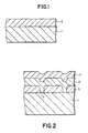
- Fig. 1 is a cross-sectional view of a layered structure employed in one stage of the method of the invention
- Fig. 2 is a cross-sectional view of a layered structure provided with seed vias formed from the structure of Fig. 1 after further processing according to the method of the invention;
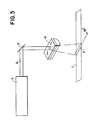
- Fig. 3 is a diagrammatic view of a zone heating source for carrying out the method of the invention.
- Fig. 4 is a planar view of the formation of the molten zones during the scanning of the layered structure employed in the method of the invention.
- soft glasses such as phosphosilicate glass, NA-40 (an almino-silicate glass produced by the Hoya Company) and 7059 glass produced by Corning Company are particularly useful.
- the thickness of the dielectric layer may be about 500 ⁇ and thicker.
- the dielectric layer may be applied to the monocrystalline silicon substrate by any appropriate means such as chemical vapor deposition or sputter deposition.
- the rectangular strips of the dielectric material may be formed in the dielectric layer by any convenient means.
- photoetching is an example of a means for forming the strips of dielectric material that has been found to be highly useful.
- the dielectric strip may be as long as will fit on the substrate.
- the dielectric strips are about 80 mm-100 mm long and about 100 ⁇ m-1000 ⁇ m wide. These strips are separated so as to leave exposed rectangular, essentially parallel strips of the monocrystalline silicon substrate preferably 10 ⁇ m-200 ⁇ m wide and 80 mm-100 mm long.
- the polycrystalline or amorphous silicon layer is deposited so as to have a thickness of up to about 10 ⁇ m and preferably from 2000 ⁇ -1.0 ⁇ m.
- a thin layer of silicon dioxide of about 1 ⁇ m to 3 ⁇ m be deposited on this layer preferably by low temperature chemical vapor deposition.
- Heating of the monocrystalline substrate may be provided by any convenient means such as a resistance heater.
- the substrate is heated to a temperature of about the softening point of the dielectric layer.
- a zone heating source such as a heat beam from a CO2 laser is focused on the strips of the polycrystalline or amorphous silicon in such a manner as to cause an elongated molten silicon zone to form with an approximately straight interface between the molten silicon and the crystal growing from the molten zone.
- elongated molten zones may be formed by focusing the laser beam with a cylindrical lens.
- the zone heating source is focused on the strips so that the molten silicon-growing crystal interface is oriented at an angle of about 10-80° and most preferably about 45° with the axis of the strips.
- the molten silicon zone is scanned by the zone heating source in a direction parallel to the axis of the strips at a rate of up to 4 mm/sec.
- a monocrystalline silicon substrate 1 a thin layer 3 of a thickness of 1 ⁇ m of a dielectric material such as phosphorsilicate glass is deposited.
- a dielectric material such as phosphorsilicate glass
- the layer of phosphosilicate glass is etched through in a pattern so as to form essentially rectangular parallel strips 5, each of said strips being separated from each other by essentially parallel rectangular 10 ⁇ m wide strips 7 of the exposed surface of the monocrystalline substrate.
- a thin film 9, of approximately 1.0 microns thick of polycrystalline silicon is then deposited on the strips 5 of the phosphosilicate glass and the exposed strips 7 of the surface of the mono-crystalline silicon substrate.
- a thin layer 11 of approximately 1.5 microns of silicon dioxide is then deposited on the layer 9 of the polycrystalline silicon.
- the resultant assembly is then placed in a heater and brought to a temperature of about 900°C. (not shown).
- a heat beam 13 having a diameter of 6.3 mm on a 50 watt CO2 laser 15 is directed by plane mirror 17 into a cylindrical lens 19 the focal length of which is 121 ⁇ m mm, and arranged so that the major axis of the resultant spot 21 focused on the polysilicon film is elliptical with the major axis of the spot being angled at 45° relative to the major axis of the exposed strips 7 of the silicon substrate.
- the spot 21 formed on the polycrystalline silicon strips forms an elongated molten zone having an essentially straight interface between the resultant silicon liquid and the growing monocrystalline silicon layer.
- the molten silicon liquid growing monocrystalline silicon interface is oriented at 45° relative to the exposed silicon substrate strips 7.
- the growth of the monocrystalline silicon layer proceeds according to the manner as shown in Fig. 4. It is believed that the growth of the monocrystalline silicon layer starts from the exposed strips of the monocrystalline silicon substrate (seed regions), proceeds by liquid phase epitaxy up from the substrate to the top of the seed regions then proceeds laterally across the strip of the phosphosilicate glass.
Landscapes
- Crystals, And After-Treatments Of Crystals (AREA)
- Recrystallisation Techniques (AREA)
- Photovoltaic Devices (AREA)
Applications Claiming Priority (2)
| Application Number | Priority Date | Filing Date | Title |
|---|---|---|---|
| US44651689A | 1989-12-05 | 1989-12-05 | |
| US446516 | 1989-12-05 |
Publications (1)
| Publication Number | Publication Date |
|---|---|
| EP0431685A1 true EP0431685A1 (fr) | 1991-06-12 |
Family
ID=23772889
Family Applications (1)
| Application Number | Title | Priority Date | Filing Date |
|---|---|---|---|
| EP90203158A Withdrawn EP0431685A1 (fr) | 1989-12-05 | 1990-11-30 | Procédé de fabrication de bandes sans défaut et de faible épaisseur de silicium monocristallin sur isolant |
Country Status (3)
| Country | Link |
|---|---|
| EP (1) | EP0431685A1 (fr) |
| JP (1) | JPH0482213A (fr) |
| KR (1) | KR910013486A (fr) |
Cited By (1)
| Publication number | Priority date | Publication date | Assignee | Title |
|---|---|---|---|---|
| GB2266993B (en) * | 1992-05-04 | 1996-01-10 | Mitsubishi Electric Corp | Method of forming single-crystal semiconductor films |
Families Citing this family (2)
| Publication number | Priority date | Publication date | Assignee | Title |
|---|---|---|---|---|
| KR100322175B1 (ko) * | 1992-07-02 | 2002-05-13 | 가나이 쓰도무 | 절연물및절연물을구비한가스절연고전압장치 |
| JP4978084B2 (ja) * | 2006-07-05 | 2012-07-18 | 日本電気株式会社 | セルラシステム及びその周波数キャリア割当方法並びにそれに用いる基地局制御装置及び基地局 |
Citations (2)
| Publication number | Priority date | Publication date | Assignee | Title |
|---|---|---|---|---|
| US4743567A (en) * | 1987-08-11 | 1988-05-10 | North American Philips Corp. | Method of forming thin, defect-free, monocrystalline layers of semiconductor materials on insulators |
| EP0346987A1 (fr) * | 1988-06-17 | 1989-12-20 | Koninklijke Philips Electronics N.V. | Méthode pour former des minces bandes monocristallines sans défauts de matériaux semi-conducteurs sur des isolants |
Family Cites Families (4)
| Publication number | Priority date | Publication date | Assignee | Title |
|---|---|---|---|---|
| JPS5839012A (ja) * | 1981-08-31 | 1983-03-07 | Fujitsu Ltd | 非単結晶半導体層の単結晶化方法 |
| JPS5979518A (ja) * | 1982-10-29 | 1984-05-08 | Hitachi Ltd | 半導体薄膜の形成方法 |
| JPS6119116A (ja) * | 1984-07-05 | 1986-01-28 | Matsushita Electronics Corp | 半導体装置の製造方法 |
| JPS61245517A (ja) * | 1985-04-23 | 1986-10-31 | Agency Of Ind Science & Technol | Soi結晶の形成方法 |
-
1990
- 1990-11-30 EP EP90203158A patent/EP0431685A1/fr not_active Withdrawn
- 1990-12-01 JP JP2402963A patent/JPH0482213A/ja active Pending
- 1990-12-03 KR KR1019900019740A patent/KR910013486A/ko not_active Withdrawn
Patent Citations (2)
| Publication number | Priority date | Publication date | Assignee | Title |
|---|---|---|---|---|
| US4743567A (en) * | 1987-08-11 | 1988-05-10 | North American Philips Corp. | Method of forming thin, defect-free, monocrystalline layers of semiconductor materials on insulators |
| EP0346987A1 (fr) * | 1988-06-17 | 1989-12-20 | Koninklijke Philips Electronics N.V. | Méthode pour former des minces bandes monocristallines sans défauts de matériaux semi-conducteurs sur des isolants |
Non-Patent Citations (2)
| Title |
|---|
| 1989 IEEE MTT-S INT. MICROWAVE SYMP. DIGEST, Long Beach, CA, 13th - 15th June 1989, vol. 1, pages 969-972, IEEE, New York, US; T.J. LETAVIC et al.: "Recrystallized silicon-on-alumina as a monolithic circuit technology" * |
| JOURNAL OF APPLIED PHYSICS, vol. 61, no. 3, 1st February 1987, pages 1006-1014; S. HORITA et al.: "Characterization of silicon-on-insulator films recrystallized by an obliquely scanned pseudoline electron beam" * |
Cited By (1)
| Publication number | Priority date | Publication date | Assignee | Title |
|---|---|---|---|---|
| GB2266993B (en) * | 1992-05-04 | 1996-01-10 | Mitsubishi Electric Corp | Method of forming single-crystal semiconductor films |
Also Published As
| Publication number | Publication date |
|---|---|
| KR910013486A (ko) | 1991-08-08 |
| JPH0482213A (ja) | 1992-03-16 |
Similar Documents
| Publication | Publication Date | Title |
|---|---|---|
| CA1333042C (fr) | Couche de revetement pour processus de recristallisation | |
| US4743567A (en) | Method of forming thin, defect-free, monocrystalline layers of semiconductor materials on insulators | |
| US4187126A (en) | Growth-orientation of crystals by raster scanning electron beam | |
| USRE33096E (en) | Semiconductor substrate | |
| US4888302A (en) | Method of reduced stress recrystallization | |
| EP0431685A1 (fr) | Procédé de fabrication de bandes sans défaut et de faible épaisseur de silicium monocristallin sur isolant | |
| US4737233A (en) | Method for making semiconductor crystal films | |
| US4576676A (en) | Thick crystalline films on foreign substrates | |
| JPS6046539B2 (ja) | シリコン結晶膜の製造方法 | |
| EP0346987A1 (fr) | Méthode pour former des minces bandes monocristallines sans défauts de matériaux semi-conducteurs sur des isolants | |
| JP2898360B2 (ja) | 半導体膜の製造方法 | |
| EP0319082A1 (fr) | Méthode pour former une couche monocristalline fine de matériau semi-conducteur sur un substrat | |
| US5891244A (en) | Apparatus for the manufacture of SOI wafer and process for preparing SOI wafer therewith | |
| Eyer et al. | Silicon sheets grown from powder layers by a zone melting process | |
| JPH0442358B2 (fr) | ||
| Givargizov et al. | Defect engineering in SOI films prepared by zone-melting recrystallization | |
| CA1254987A (fr) | Fabrication d'un dispositif semiconducteur de forte superficie | |
| JPS58114420A (ja) | 単結晶シリコン膜の形成法 | |
| JPS5886716A (ja) | 単結晶半導体膜形成法 | |
| JPS59182518A (ja) | マイクロ帯域溶融法 | |
| JP2683005B2 (ja) | 誘電体分離基板の製造方法 | |
| Celler et al. | Thick films for dielectric isolation by lateral epitaxy from the melt | |
| Inoue et al. | Electron-beam recrystallization of silicon layers on silicon dioxide | |
| JPH03138925A (ja) | 半導体膜の結晶化法 | |
| JPH03116924A (ja) | 単結晶半導体薄膜の製造方法 |
Legal Events
| Date | Code | Title | Description |
|---|---|---|---|
| PUAI | Public reference made under article 153(3) epc to a published international application that has entered the european phase |
Free format text: ORIGINAL CODE: 0009012 |
|
| AK | Designated contracting states |
Kind code of ref document: A1 Designated state(s): DE FR GB IT NL |
|
| STAA | Information on the status of an ep patent application or granted ep patent |
Free format text: STATUS: THE APPLICATION IS DEEMED TO BE WITHDRAWN |
|
| 18D | Application deemed to be withdrawn |
Effective date: 19911213 |