EP0431761A2 - CMOS-Taktgeberanordnung - Google Patents
CMOS-Taktgeberanordnung Download PDFInfo
- Publication number
- EP0431761A2 EP0431761A2 EP90312308A EP90312308A EP0431761A2 EP 0431761 A2 EP0431761 A2 EP 0431761A2 EP 90312308 A EP90312308 A EP 90312308A EP 90312308 A EP90312308 A EP 90312308A EP 0431761 A2 EP0431761 A2 EP 0431761A2
- Authority
- EP
- European Patent Office
- Prior art keywords
- phase clock
- clock signal
- transistor
- node
- output
- Prior art date
- Legal status (The legal status is an assumption and is not a legal conclusion. Google has not performed a legal analysis and makes no representation as to the accuracy of the status listed.)
- Granted
Links
Images

Classifications
-
- H—ELECTRICITY
- H03—ELECTRONIC CIRCUITRY
- H03K—PULSE TECHNIQUE
- H03K19/00—Logic circuits, i.e. having at least two inputs acting on one output; Inverting circuits
- H03K19/0021—Modifications of threshold
- H03K19/0027—Modifications of threshold in field effect transistor circuits
-
- H—ELECTRICITY
- H03—ELECTRONIC CIRCUITRY
- H03K—PULSE TECHNIQUE
- H03K5/00—Manipulating of pulses not covered by one of the other main groups of this subclass
- H03K5/15—Arrangements in which pulses are delivered at different times at several outputs, i.e. pulse distributors
- H03K5/15006—Arrangements in which pulses are delivered at different times at several outputs, i.e. pulse distributors with two programmable outputs
Definitions
- This invention relates generally to timing or clocking circuitry for use with integrated circuits and more particularly, it relates to a CMOS clock generator for generating internal CMOS phase clock signals having an adjustable overlap voltage.
- CMOS clock generator used with integrated logic circuits for generating internal CMOS phase clock signals in which the overlap voltage is adjustable.
- the CMOS clock generator of the present invention includes means for adjusting the clock overlap voltage either up or down to speed up or slow down a chip after fabrication. This technique utilizes a laser to break or open up fuses connected to electrodes of transistor devices.
- CMOS clock generator for generating internal CMOS phase clock signals which is relatively simple and economical to manufacture and assemble.
- CMOS clock generator for use with integrated logic circuits for generating internal CMOS phase clock signals in which the overlap voltage is adjustable.
- CMOS clock generator which includes means for adjusting the clock overlap voltage either up or down to speed up or slow down a semiconductor chip after fabrication.
- CMOS clock generator for generating internal CMOS phase clock signals in which the overlap voltage is adjustable by a laser to break or open up fuses connected to electrodes of transistor devices.
- CMOS clock generator for generating internal CMOS phase clock signals having an adjustable overlap voltage which includes a first circuit having a first input responsive to an input clock signal for generating a first phase clock signal on its output and a second circuit having a first input responsive to the input clock signal for generating a second phase clock signal on its output.
- the first circuit has a second input responsive to the second phase clock signal at the output of the second circuit for controlling the overlap voltage.
- the second circuit has a second input responsive to the first phase clock signal at the output of the first circuit for controlling the overlap voltage.
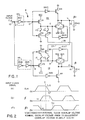
- FIG. 1 is a schematic circuit diagram of a CMOS clock generator embodying the present invention
- Figures 2(a)-2(c) are waveforms useful in understanding the operation of Figure 1;
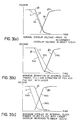
- Figures 3(a)-3(c) are plots of the voltages at the node C of Figure 1 relative to the voltages of the true phase clock signal dependent upon the ratio of the sizes of the transistors N1a-N1n and N2a-N2n;
- Figures 4(a)-4(d) are schematic circuit diagrams showing how each of the transistors N5, N6, N1 and N2 and associated fuses may be implemented as a plurality of transistors N5a-N5n; N6a-N6n; N1a-N1n; and N2a-N2n, respectively with their associated fuses.
- FIG. 1 a schematic circuit diagram of a CMOS clock generator 8 for generating a first or true internal CMOS level phase clock signal ⁇ 1 at node X on output line 10 and a second or complementary internal CMOS level phase clock signal ⁇ 2 at node Y on output line 14.
- the CMOS clock generator 8 has an input at node Z connected to an input line 12 for receiving an external input clock signal CLK.
- the clock generator 8 is formed of a first delay circuit 16, a first phase clock generating circuit 18, a second delay circuit 20 and a second phase clock generating circuit 22.
- the first delay circuit 16 is formed of a pair of series-connected inverters INV4 and INV5, and the second delay circuit 20 is formed of a single inverter INV1.
- the first phase clock generating circuit 18 has a first input connected to the output of the inverter INV5 and a second input coupled to the output line 14 via line 24 and the node Y.
- the output of the first phase clock generating circuit 18 is defined by the node X.
- a capacitive load represented by a capacitor CPH1 is connected between the node X and a ground potential.
- the second phase clock generating circuit 22 has a first input connected to the output of the inverter INV1 and a second input coupled to the output line 10 via line 26 and the node X.
- the output of the second phase clock generating circuit 22 is defined by the node Y.
- a capacitive load represented by a capacitor CPH2 is connected between the node Y and the ground potential.
- the first phase clock generating circuit 18 includes a first P-channel transistor P3, a first N-channel transistor N5, and a second N-channel transistor N6.
- the transistor P3 has its source connected to a supply potential VCC, which is typically at+5.0 volts, and its drain connected to an internal node A.
- the transistor N5 has its source connected to the ground potential and its drain connected via a fuse F1 to the node A.
- the transistor N6 has its source connected via the line 24 to the output of the second phase clock generating circuit 22 at the node Y and its drain connected via a fuse F2 to the node A.
- the gates of the transistors P3, N5 and N6 are all connected together and to an internal node B defining the input of the first phase clock generating circuit 18.
- the fuses F1 and F2 may, for example, be metal, silicide or a semiconductor such as polysilicon material which may be opened or blown by the use of a laser cut.
- the first phase clock generating circuit 18 further includes inverters INV6, INV7; a first pull-up transistor P4; a second pull-up transistor N7; and a pull-down transistor N8.
- the transistor P4 has its source connected to the supply potential VCC and its drain connected to the source and drain of the respective transistors N7 and N8 and to the node X.
- the transistor N7 has also its drain connected to the supply potential VCC.
- the transistor N8 has its source connected to the ground potential.
- the inverter INV7 has its input connected to the gate of the transistor P4 at the node A and its output connected to the gate of the transistor N7.
- the inverter INV6 has its input connected to the node B and its output connected to the gate of the transistor N8.
- the second phase clock generating circuit 22 includes a first P-channel transistor P1, a first N-channel transistor N1, and a second N-channel transistor N2.
- the transistor P1 has its source connected to the supply potential VCC and its drain connected to an internal node C.
- the transistor N1 has its source connected to the ground potential and its drain connected via a fuse F3 to the node C.
- the transistor N2 has its source connected via the line 26 to the output of the first phase clock generating circuit 18 at the node X and its drain connected via a fuse F4 to the node C.
- the gates of the transistors P1, N1 and N2 are all connected together and to an internal node D defining the input of the second phase clock generating circuit 22.
- the fuses F3 and F4 may, for example, be metal, silicide or a semiconductor such as polysilicon material which may be opened or blown by the use of a laser cut.
- the second phase clock generating circuit 22 further includes INV2, INV3; a first pull-up transistor P2; a second pull-up transistor N3; and a pull-down transistor N4.
- the transistor P2 has its source connected to the supply potential VCC and its drain connected to the source and drain of the respective transistors N3 and N4 and to the node Y.
- the transistor N3 has also its drain connected to the supply potential VCC.
- the transistor N4 has its source connected to the ground potential.
- the inverter INV3 has its input connected to the gate of the transistor P2 at the node C and its output connected to the gate of the transistor N3.
- the inverter INV2 has its input connected to the node D and its output connected to the gate of the transistor N4.
- the output of the first phase clock generating circuit 18 at the node X provides a feedback control voltage which is fed via the line 26 as the second input to the second phase clock generating circuit 22.
- the output of the second phase clock generating circuit 22 at the node Y provides a feedback control signal which is fed via the line 24 as the second input to the first phase clock generating circuit 18.
- the feedback control voltages from the outputs of the respective clock generating circuits 18 and 22 are utilized to control the rising edge of the other output or to control thus the overlap voltage.
- the N-channel transistors N5 and N6 When the input clock signal CLK makes a high-to-low transition at time t1a, the N-channel transistors N5 and N6 will be turned off, the P-channel transistor P3 will be turned on and the output of the inverter INV6 will change to a high or "1" logic level. This will, in turn, cause the pull-up transistors P4 and N7 to be turned off and cause the pull-down transistor N8 to be turned on. As a result, the true phase clock signal ⁇ 1 on the output line 10 will begin making a high-to-low transition at time t2.
- the voltage on the node C is also used to drive the gate of the pull-up transistor P2 and the gate of the pull-up transistor N3 via the inverter INV3.
- the size of the transistor N2 to be larger than the size of the transistor N1, the voltage at the node C will discharge only slightly when the transistors N1 and N2 are turned on initially and will not decrease further until the voltage on the output line 10 begins to discharge.
- the purpose of the transistor N3 is to limit the overshoot when the node Y is making a low-to-high transition by increasing the output impedance and to reduce current to the node Y at the time t1a when the node C is decreased somewhat. Consequently, the complementary phase clock signal ⁇ 2 on the output line 14 will make a low-to-high transition at the time t3.
- the transistor N5 may be constructed alternately as a plurality of individual transistors N5a, N5b,...N5n connected in parallel as shown in Figure 4(a). Further, the associated fuse F1 may be replaced with a corresponding plurality of fuses F1a, F1b,...F1n. As can be seen, all of the source electrodes of the respective plurality of transistors N5a, N5b,...N5n are connected together and to a lead line 28a which is connectible to the ground potential. All of the gate electrodes of these transistors are connected together and to a lead line 30a which is connectible to the input of the first phase clock generating circuit 18 at the node B.
- the drain electrodes of the respective transistors N5a, N5b,...N5n are connected via a corresponding one of the plurality of fuses F1a, F1b,...F1n to a lead line 32a which is connectible to the internal node A.
- the transistor N6 may be constructed alternately as a plurality of individual transistors N6a, N6b,...N6n connected in parallel as shown in Figure 4(b). Further, the associated fuse F2 may be replaced with a corresponding plurality of fuses F2a, F2b,...F2n. As can be seen, all of the source electrodes of the respective plurality of transistors N6a, N6b,...N6n are connected together and to a lead line 28b, which is connectible to the output of the second phase clock generating circuit 22 on the line 24. All of the gate electrodes of the transistors are connected together and to a lead line 30b which is connectible to the input of the first phase clock generating circuit 18 at the node B.
- the drain electrodes of the respective transistors N6a, N6b, ...N6n are connected via a corresponding one of the plurality of fuses F2a, F2b,...F2n to a lead line 32b which is connectible to the internal node A.
- the transistor N1 may be constructed alternately as a plurality of individual transistors N1a, N1b,...N1n connected in parallel as shown in Figure 4(c).
- the associated fuse F3 may be replaced with a corresponding plurality of fuses F3a, F3b,...F3n.
- all of the source electrodes of the respective plurality of transistors N1a, N1b,...N1n are connected together and to a lead line 28c which is connectible to the ground potential.
- All of the gate electrodes of these transistors are connected together and to a lead line 30c which is connectible to the input of the second phase clock generating circuit 22 at the node D.
- the drain electrodes of the respective transistors N1a, N1b,...N1n are connected via a corresponding one of the plurality of fuses F3a, F3b,...F3n to a lead line 32c which is connectible to the internal node C.
- the transistor N2 may be constructed alternately as a plurality of individual transistors N2a, N2b,...N2n connected in parallel as shown in Figure 4(d).
- the associated fuse F4 may be replaced with a corresponding plurality of fuses F4a, F4b,...F4n.
- all of the source electrodes of the respective plurality of transistors N2a, N2b,...N2n are connected together and to a lead line 28d, which is connectible to the output of the first phase clock generating circuit 18 on the line 26.
- All of the gate electrodes of the transistors are connected together and to a lead line 30d which is connectible to the input of the second phase clock generating circuit 22 at the node D.
- the drain electrodes of the respective transistors N2a, N2b, ...N2n are connected via a corresponding one of the plurality of fuses F4a, F4b,...F4n to a lead line 32d which is connectible to the internal node C.
- each of the transistors N5, N6, N1 and N2 and each of the associated fuses F1, F2, F3 and F4 being implemented as described above as a plurality of individual transistors and fuses, there is provided a means for adjusting or controlling over a relatively wide range the amount of clock overlap voltage between the internal phase clock signals ⁇ 1 and ⁇ 2.
- the overlap voltage is selectively adjusted or controlled by blowing or opening by a laser cut certain ones of the plurality of fuses one at a time in a first predetermined order so as to increase the amount of overlap voltage or in a second predetermined order so as to decrease the amount of overlap voltage.
- the ratio of the resistance between the plurality of transistors N5a-N5n and N6a-N6n (or the plurality of transistors N1a-N1n and N2a-N2n) can be selectively controlled.
- FIGS 3(a)-3(c) there are illustrated plots of the voltages at the node C of Figure 1 relative to the true and complementary phase clock signals ⁇ 1 and ⁇ 2.
- FIG 3(a) the voltage at the node C (dotted curve 34) relative to the true clock signal ⁇ 1 (curve 36) and the complementary clock signal ⁇ 2 (curve 38) prior to any adjustments being made.
- none of the plurality of fuses F1a-F1n, F2a-F2n, F3a-F3n, and F4a-F4n have been blow or opened.
- the voltage at the node C (curve 34) is slightly leading the voltage of the true phase clock signal ⁇ 1 on the output line 10.
- the amount of nominal overlap voltage between the trailing edge of the true phase clock signal ⁇ 1 and the leading edge of the complementary phase clock signal ⁇ 2 is approximately VCC/4.
- the plurality of fuses F3a-F3n would be blown initially by a laser cut one fuse at a time. Then, the plurality of fuses F4a-F4n would be blown by a laser cut again one at a time until only one fuse (i.e., F4n) is remaining. As each one of the plurality of fuses is blown, the voltage at the node C will gradually lead the voltage of the true phase clock signal ⁇ 1 less and less and will eventually lag the voltage of the clock signal ⁇ 1 more and more.
- the plurality of fuses F4a-F4n would be blown by a laser cut one fuse at a time. As each one additional fuse is blown, the voltage at the node C will lead the voltage of the true phase clock signal ⁇ 1 more and more.
- the voltage on the node C (dotted curve 34b) will appear as illustrated in Figure 3(c) as leading the voltage of the true phase clock signal ⁇ 1.
- the present invention provides an improved CMOS clock generator for use with integrated circuits for generating internal CMOS phase clock signals having an adjustable overlap voltage.
- the overlap voltage between the internal phase clock signals is adjusted either up or down to speed up or slow down a semiconductor chip after fabrication. This is achieved by the utilization of a laser to break or open up fuses connected to electrodes of transistor devices.
Landscapes
- Physics & Mathematics (AREA)
- Mathematical Physics (AREA)
- Engineering & Computer Science (AREA)
- Computer Hardware Design (AREA)
- Computing Systems (AREA)
- General Engineering & Computer Science (AREA)
- Nonlinear Science (AREA)
- Design And Manufacture Of Integrated Circuits (AREA)
- Manipulation Of Pulses (AREA)
- Oscillators With Electromechanical Resonators (AREA)
- Nitrogen Condensed Heterocyclic Rings (AREA)
- Medicines Containing Antibodies Or Antigens For Use As Internal Diagnostic Agents (AREA)
- Pharmaceuticals Containing Other Organic And Inorganic Compounds (AREA)
Applications Claiming Priority (2)
| Application Number | Priority Date | Filing Date | Title |
|---|---|---|---|
| US07/445,245 US5041738A (en) | 1989-12-04 | 1989-12-04 | CMOS clock generator having an adjustable overlap voltage |
| US445245 | 1989-12-04 |
Publications (3)
| Publication Number | Publication Date |
|---|---|
| EP0431761A2 true EP0431761A2 (de) | 1991-06-12 |
| EP0431761A3 EP0431761A3 (en) | 1992-01-22 |
| EP0431761B1 EP0431761B1 (de) | 1997-07-23 |
Family
ID=23768143
Family Applications (1)
| Application Number | Title | Priority Date | Filing Date |
|---|---|---|---|
| EP90312308A Expired - Lifetime EP0431761B1 (de) | 1989-12-04 | 1990-11-12 | CMOS-Taktgeberanordnung |
Country Status (5)
| Country | Link |
|---|---|
| US (1) | US5041738A (de) |
| EP (1) | EP0431761B1 (de) |
| JP (1) | JP3041385B2 (de) |
| AT (1) | ATE155943T1 (de) |
| DE (1) | DE69031112D1 (de) |
Cited By (3)
| Publication number | Priority date | Publication date | Assignee | Title |
|---|---|---|---|---|
| EP0529328A3 (en) * | 1991-07-29 | 1993-06-09 | Fujitsu Limited | Pulse generator circuit for producing simultaneous complementary output pulses |
| US5270580A (en) * | 1991-07-29 | 1993-12-14 | Fujitsu Limited | Pulse generator circuit for producing simultaneous complementary output pulses |
| US5986491A (en) * | 1996-05-06 | 1999-11-16 | Siemens Aktiengesellschaft | Clock signal generator |
Families Citing this family (24)
| Publication number | Priority date | Publication date | Assignee | Title |
|---|---|---|---|---|
| US5204559A (en) * | 1991-01-23 | 1993-04-20 | Vitesse Semiconductor Corporation | Method and apparatus for controlling clock skew |
| US5444405A (en) * | 1992-03-02 | 1995-08-22 | Seiko Epson Corporation | Clock generator with programmable non-overlapping clock edge capability |
| US5491432A (en) * | 1992-08-07 | 1996-02-13 | Lsi Logic Corporation | CMOS Differential driver circuit for high offset ground |
| US5345195A (en) * | 1992-10-22 | 1994-09-06 | United Memories, Inc. | Low power Vcc and temperature independent oscillator |
| KR0135735B1 (ko) * | 1992-11-04 | 1998-05-15 | 기다오까 다까시 | 소음발생을 억제하는 개량된 출력 드라이버 회로 및 번인테스트를 위한 개량된 반도체 집적회로 장치 |
| US5389831A (en) * | 1992-12-17 | 1995-02-14 | Vlsi Technology, Inc. | Clock generator for providing a pair of nonoverlapping clock signals with adjustable skew |
| JPH0738408A (ja) * | 1993-07-19 | 1995-02-07 | Sharp Corp | バッファ回路 |
| US5424661A (en) * | 1993-08-12 | 1995-06-13 | Winbond Electronics North America Corp. | Sensor circuit |
| JP3441780B2 (ja) * | 1994-02-21 | 2003-09-02 | 日本テキサス・インスツルメンツ株式会社 | クロック信号生成回路 |
| DE19548629C1 (de) * | 1995-12-23 | 1997-07-24 | Itt Ind Gmbh Deutsche | Komplementäres Taktsystem |
| US6381704B1 (en) | 1998-01-29 | 2002-04-30 | Texas Instruments Incorporated | Method and apparatus for altering timing relationships of non-overlapping clock signals in a microprocessor |
| US6172522B1 (en) * | 1998-08-13 | 2001-01-09 | International Business Machines Corporation | Slew rate controlled predriver circuit |
| US6163169A (en) * | 1998-08-13 | 2000-12-19 | International Business Machines Corporation | CMOS tri-state control circuit for a bidirectional I/O with slew rate control |
| JP3789241B2 (ja) * | 1998-12-01 | 2006-06-21 | Necエレクトロニクス株式会社 | バイアス回路及び半導体記憶装置 |
| JP3478996B2 (ja) | 1999-06-01 | 2003-12-15 | Necエレクトロニクス株式会社 | 低振幅ドライバ回路及びこれを含む半導体装置 |
| JP2002026265A (ja) * | 2000-07-06 | 2002-01-25 | Toshiba Lsi System Support Kk | 半導体集積回路およびその配置設計方法 |
| US6459318B1 (en) * | 2001-03-22 | 2002-10-01 | Hewlett-Packard Company | Programmable delay clock gaters |
| US6424190B1 (en) * | 2001-09-13 | 2002-07-23 | Broadcom Corporation | Apparatus and method for delay matching of full and divided clock signals |
| US6774683B2 (en) * | 2002-08-13 | 2004-08-10 | Analog Devices, Inc. | Control loop for minimal tailnode excursion of differential switches |
| JP2004320231A (ja) * | 2003-04-14 | 2004-11-11 | Renesas Technology Corp | 半導体装置の出力回路 |
| KR100596977B1 (ko) * | 2004-08-20 | 2006-07-05 | 삼성전자주식회사 | 외부 기준 전압과 내부 기준 전압을 동시에 이용하는 기준전압 발생 회로 및 이를 이용한 기준 전압 발생 방법 |
| KR101456207B1 (ko) * | 2013-08-05 | 2014-11-03 | 숭실대학교산학협력단 | 스위칭 커패시터를 이용한 슬루 레이트 조절 장치 |
| TWI658697B (zh) * | 2018-08-02 | 2019-05-01 | 崛智科技有限公司 | 資料閂鎖電路及其脈波信號產生器 |
| US20260066889A1 (en) * | 2024-09-04 | 2026-03-05 | Globalfoundries U.S. Inc. | Low-power low-area deadtime generator |
Family Cites Families (5)
| Publication number | Priority date | Publication date | Assignee | Title |
|---|---|---|---|---|
| GB2030807B (en) * | 1978-10-02 | 1982-11-10 | Ibm | Latch circuit |
| JPS62188096A (ja) * | 1986-02-13 | 1987-08-17 | Toshiba Corp | 半導体記憶装置のリフレツシユ動作タイミング制御回路 |
| JPS63136815A (ja) * | 1986-11-28 | 1988-06-09 | Mitsubishi Electric Corp | 周期信号発生回路 |
| US4855617A (en) * | 1986-12-19 | 1989-08-08 | Texas Instruments Incorporated | Schottky transistor logic floating latch flip-flop |
| US4950920A (en) * | 1987-09-30 | 1990-08-21 | Kabushiki Kaisha Toshiba | Complementary signal output circuit with reduced skew |
-
1989
- 1989-12-04 US US07/445,245 patent/US5041738A/en not_active Expired - Fee Related
-
1990
- 1990-11-12 AT AT90312308T patent/ATE155943T1/de not_active IP Right Cessation
- 1990-11-12 DE DE69031112T patent/DE69031112D1/de not_active Expired - Lifetime
- 1990-11-12 EP EP90312308A patent/EP0431761B1/de not_active Expired - Lifetime
- 1990-11-30 JP JP2341179A patent/JP3041385B2/ja not_active Expired - Lifetime
Cited By (4)
| Publication number | Priority date | Publication date | Assignee | Title |
|---|---|---|---|---|
| EP0529328A3 (en) * | 1991-07-29 | 1993-06-09 | Fujitsu Limited | Pulse generator circuit for producing simultaneous complementary output pulses |
| US5270580A (en) * | 1991-07-29 | 1993-12-14 | Fujitsu Limited | Pulse generator circuit for producing simultaneous complementary output pulses |
| US5986491A (en) * | 1996-05-06 | 1999-11-16 | Siemens Aktiengesellschaft | Clock signal generator |
| EP0897614B1 (de) * | 1996-05-06 | 2000-11-08 | Siemens Aktiengesellschaft | Taktsignalgenerator |
Also Published As
| Publication number | Publication date |
|---|---|
| EP0431761B1 (de) | 1997-07-23 |
| US5041738A (en) | 1991-08-20 |
| JP3041385B2 (ja) | 2000-05-15 |
| ATE155943T1 (de) | 1997-08-15 |
| DE69031112D1 (de) | 1997-09-04 |
| JPH03190416A (ja) | 1991-08-20 |
| EP0431761A3 (en) | 1992-01-22 |
Similar Documents
| Publication | Publication Date | Title |
|---|---|---|
| US5041738A (en) | CMOS clock generator having an adjustable overlap voltage | |
| US6064227A (en) | Output buffer circuit having low breakdown voltage | |
| JP3980431B2 (ja) | バッファ回路とバッファツリー及び半導体装置 | |
| US5576656A (en) | Voltage regulator for an output driver with reduced output impedance | |
| JPH07114359B2 (ja) | 半導体集積回路 | |
| US5055713A (en) | Output circuit of semiconductor integrated circuit | |
| US6559676B1 (en) | Output buffer circuit | |
| EP0270300A2 (de) | Statische PLA- oder ROM-Schaltung mit selbsterzeugtem Vorladen | |
| JP7534590B2 (ja) | 放電制御回路 | |
| US6380770B1 (en) | Low ground bounce and low power supply bounce output driver with dual, interlocked, asymmetric delay lines | |
| US5808492A (en) | CMOS bidirectional buffer without enable control signal | |
| US6825699B2 (en) | Charge pump circuit, passive buffer that employs the charge pump circuit, and pass gate that employs the charge pump circuit | |
| US7030673B2 (en) | Phase splitter circuit | |
| US7098704B2 (en) | Semiconductor integrated circuit device | |
| JPS63246925A (ja) | Cmos論理回路 | |
| KR960016434B1 (ko) | 노이즈 경감회로를 갖는 출력버퍼회로 | |
| JPH0254698B2 (de) | ||
| JP3166740B2 (ja) | 論理回路 | |
| US4636657A (en) | High speed CMOS clock generator | |
| CA2228243C (en) | A single-edge adjustable delay circuit | |
| US20060170478A1 (en) | Delay circuit for semiconductor device | |
| US4950928A (en) | Dynamic PLA circuit with no "virtual grounds" | |
| JP2767909B2 (ja) | 出力バッファ回路 | |
| JPH0353715A (ja) | 出力バッファ回路 | |
| KR960009398B1 (ko) | 출력 버퍼 회로 |
Legal Events
| Date | Code | Title | Description |
|---|---|---|---|
| PUAI | Public reference made under article 153(3) epc to a published international application that has entered the european phase |
Free format text: ORIGINAL CODE: 0009012 |
|
| AK | Designated contracting states |
Kind code of ref document: A2 Designated state(s): AT BE CH DE DK ES FR GB GR IT LI LU NL SE |
|
| PUAL | Search report despatched |
Free format text: ORIGINAL CODE: 0009013 |
|
| AK | Designated contracting states |
Kind code of ref document: A3 Designated state(s): AT BE CH DE DK ES FR GB GR IT LI LU NL SE |
|
| 17P | Request for examination filed |
Effective date: 19920629 |
|
| 17Q | First examination report despatched |
Effective date: 19950929 |
|
| GRAG | Despatch of communication of intention to grant |
Free format text: ORIGINAL CODE: EPIDOS AGRA |
|
| GRAH | Despatch of communication of intention to grant a patent |
Free format text: ORIGINAL CODE: EPIDOS IGRA |
|
| GRAH | Despatch of communication of intention to grant a patent |
Free format text: ORIGINAL CODE: EPIDOS IGRA |
|
| GRAA | (expected) grant |
Free format text: ORIGINAL CODE: 0009210 |
|
| AK | Designated contracting states |
Kind code of ref document: B1 Designated state(s): AT BE CH DE DK ES FR GB GR IT LI LU NL SE |
|
| PG25 | Lapsed in a contracting state [announced via postgrant information from national office to epo] |
Ref country code: GR Free format text: LAPSE BECAUSE OF FAILURE TO SUBMIT A TRANSLATION OF THE DESCRIPTION OR TO PAY THE FEE WITHIN THE PRESCRIBED TIME-LIMIT Effective date: 19970723 Ref country code: LI Effective date: 19970723 Ref country code: FR Effective date: 19970723 Ref country code: ES Free format text: THE PATENT HAS BEEN ANNULLED BY A DECISION OF A NATIONAL AUTHORITY Effective date: 19970723 Ref country code: DK Effective date: 19970723 Ref country code: IT Free format text: LAPSE BECAUSE OF FAILURE TO SUBMIT A TRANSLATION OF THE DESCRIPTION OR TO PAY THE FEE WITHIN THE PRE;WARNING: LAPSES OF ITALIAN PATENTS WITH EFFECTIVE DATE BEFORE 2007 MAY HAVE OCCURRED AT ANY TIME BEFORE 2007. THE CORRECT EFFECTIVE DATE MAY BE DIFFERENT FROM THE ONE RECORDED.SCRIBED TIME-LIMIT Effective date: 19970723 Ref country code: NL Free format text: LAPSE BECAUSE OF FAILURE TO SUBMIT A TRANSLATION OF THE DESCRIPTION OR TO PAY THE FEE WITHIN THE PRESCRIBED TIME-LIMIT Effective date: 19970723 Ref country code: CH Effective date: 19970723 Ref country code: AT Effective date: 19970723 Ref country code: BE Effective date: 19970723 |
|
| REF | Corresponds to: |
Ref document number: 155943 Country of ref document: AT Date of ref document: 19970815 Kind code of ref document: T |
|
| REG | Reference to a national code |
Ref country code: CH Ref legal event code: EP |
|
| REF | Corresponds to: |
Ref document number: 69031112 Country of ref document: DE Date of ref document: 19970904 |
|
| PG25 | Lapsed in a contracting state [announced via postgrant information from national office to epo] |
Ref country code: SE Effective date: 19971023 |
|
| PG25 | Lapsed in a contracting state [announced via postgrant information from national office to epo] |
Ref country code: DE Effective date: 19971024 |
|
| PG25 | Lapsed in a contracting state [announced via postgrant information from national office to epo] |
Ref country code: LU Free format text: LAPSE BECAUSE OF NON-PAYMENT OF DUE FEES Effective date: 19971112 |
|
| EN | Fr: translation not filed | ||
| NLV1 | Nl: lapsed or annulled due to failure to fulfill the requirements of art. 29p and 29m of the patents act | ||
| REG | Reference to a national code |
Ref country code: CH Ref legal event code: PL |
|
| PLBE | No opposition filed within time limit |
Free format text: ORIGINAL CODE: 0009261 |
|
| STAA | Information on the status of an ep patent application or granted ep patent |
Free format text: STATUS: NO OPPOSITION FILED WITHIN TIME LIMIT |
|
| 26N | No opposition filed | ||
| REG | Reference to a national code |
Ref country code: GB Ref legal event code: IF02 |
|
| PGFP | Annual fee paid to national office [announced via postgrant information from national office to epo] |
Ref country code: GB Payment date: 20021002 Year of fee payment: 13 |
|
| PG25 | Lapsed in a contracting state [announced via postgrant information from national office to epo] |
Ref country code: GB Free format text: LAPSE BECAUSE OF NON-PAYMENT OF DUE FEES Effective date: 20031112 |
|
| GBPC | Gb: european patent ceased through non-payment of renewal fee |
Effective date: 20031112 |