EP0433032A2 - Appareil de reproduction de signal - Google Patents
Appareil de reproduction de signal Download PDFInfo
- Publication number
- EP0433032A2 EP0433032A2 EP90313473A EP90313473A EP0433032A2 EP 0433032 A2 EP0433032 A2 EP 0433032A2 EP 90313473 A EP90313473 A EP 90313473A EP 90313473 A EP90313473 A EP 90313473A EP 0433032 A2 EP0433032 A2 EP 0433032A2
- Authority
- EP
- European Patent Office
- Prior art keywords
- output
- signal
- frequency
- circuit
- modulation wave
- Prior art date
- Legal status (The legal status is an assumption and is not a legal conclusion. Google has not performed a legal analysis and makes no representation as to the accuracy of the status listed.)
- Withdrawn
Links
Images



Classifications
-
- H—ELECTRICITY
- H04—ELECTRIC COMMUNICATION TECHNIQUE
- H04N—PICTORIAL COMMUNICATION, e.g. TELEVISION
- H04N5/00—Details of television systems
- H04N5/76—Television signal recording
- H04N5/91—Television signal processing therefor
- H04N5/911—Television signal processing therefor for the suppression of noise
-
- H—ELECTRICITY
- H03—ELECTRONIC CIRCUITRY
- H03D—DEMODULATION OR TRANSFERENCE OF MODULATION FROM ONE CARRIER TO ANOTHER
- H03D3/00—Demodulation of angle-, frequency- or phase- modulated oscillations
- H03D3/001—Details of arrangements applicable to more than one type of frequency demodulator
- H03D3/002—Modifications of demodulators to reduce interference by undesired signals
-
- H—ELECTRICITY
- H04—ELECTRIC COMMUNICATION TECHNIQUE
- H04N—PICTORIAL COMMUNICATION, e.g. TELEVISION
- H04N5/00—Details of television systems
- H04N5/76—Television signal recording
- H04N5/91—Television signal processing therefor
- H04N5/92—Transformation of the television signal for recording, e.g. modulation, frequency changing; Inverse transformation for playback
- H04N5/9201—Transformation of the television signal for recording, e.g. modulation, frequency changing; Inverse transformation for playback involving the multiplexing of an additional signal and the video signal
- H04N5/9202—Transformation of the television signal for recording, e.g. modulation, frequency changing; Inverse transformation for playback involving the multiplexing of an additional signal and the video signal the additional signal being a sound signal
- H04N5/9204—Transformation of the television signal for recording, e.g. modulation, frequency changing; Inverse transformation for playback involving the multiplexing of an additional signal and the video signal the additional signal being a sound signal using frequency division multiplex
Definitions
- the present invention relates to a signal reproducing apparatus for removing cross modulation interference components due to secondary distortion or tertiary distortion generated during recording and reproducing in a video disc system, a video tape recorder or the like.
- the reproduced video FM signal is further phase-modulated to reduce the cross modulation interference.
- the cross modulation level differs significantly from one disk to other, and even in a same disk, the cross modulation level varies between the outer circumference and inner circumference. So, the cross modulation could not be removed satisfactorily in the conventional methods, and there was a case that the cross modulation interference was increased.
- the present invention provides a signal reproducing apparatus for reproducing a video signal from a recording medium having recorded therein a mixed signal of a first modulation wave having a video signal frequency-modulated by a carrier frequency fc, and a second modulation wave having a second signal modulated in a lower frequency region than said frequency fc, which comprises:
- frequency demodulation means for frequency-demodulating the first modulation wave, and having means for reducing the cross modulation interference generated in the demodulated signal depending on an output from detecting means;
- first filter means for separating the second modulation wave from the reproduced signal
- the detecting means for detecting a cross modulation interference component remaining in the demodulated signal in a specified period from an output signal of the first filter means and an output of the frequency demodulation means, wherein
- a closed loop for controlling the frequency demodulation means by the output of the detecting means is composed so as to remove the cross modulation interference components in the frequency demodulated signal of the output of the frequency demodulation means.
- a preferred signal reproducing means comprises:
- frequency demodulation means for frequency-demodulating the first modulation wave
- first filter means for separating the second modulation signal from the reproduced signal
- gain adjusting means for adjusting the gain of an output signal of the first filter means by information from a detecting means
- subtracting means for subtracting an output signal of the gain adjusting means from an output of the demodulation means
- the detecting means for detecting the second modulation wave component remaining in an output signal of the subtracting means in a specified period by feeding the output signal of the subtracting means and the output signal of the first filter means, wherein
- a closed loop for controlling the gain adjusting means by the output of the detecting means is composed so as to remove the second modulation wave component in the frequency demodulated signal of the output of the subtracting means.
- Another preferred signal reproducing apparatus comprises:
- frequency demodulation means for frequency-demodulating the first modulation wave
- first filter means for separating the second modulation wave from the reproduced signal
- doubling means for doubling the frequency of an output signal of the first filter means
- gain adjusting means for adjusting the gain of an output signal of the doubling means by information from a detecting means
- subtracting means for subtracting an output signal of the gain adjusting means from an output of the demodulation means
- the detecting means for detecting the double frequency component of the second modulation wave remaining in an output signal of the subtracting means in a specified period by feeding the output signal of the subtracting means and the output signal of the doubling means, wherein
- a closed loop for controlling the gain adjusting means by the output of the detecting means is composed so as to remove the double frequency component of the second modulation wave in the frequency demodulated signal of the output of the subtracting means.
- a further different preferred signal reproducing apparatus comprises:
- frequency demodulation means capable of controlling the limiter balance for frequency modulating the first modulation wave
- detecting means for detecting the second modulation wave component remaining in a specified period of an output signal of a frequency demodulation circuit by feeding the output signal of the frequency demodulation circuit and an output signal of the first filter, wherein
- a closed loop for controlling the limiter balance of the frequency demodulation circuit by the output of the detecting means is composed so as to suppress the second modulation wave component occurring in the frequency demodulated signal of the output of the frequency demodulation circuit.
- Another preferred signal reproducing apparatus comprises:
- frequency demodulation means for frequency-demodulating the first modulation wave
- detecting means for detecting the second modulation wave component remaining in an output signal of the frequency demodulation means in a specified period by feeding the output signal of the frequency demodulation means and an output signal of the first filter
- the frequency demodulation means comprises a limiter circuit for limiting the first modulation wave, a first pulse generation circuit for generating a pulse of a specific width in response to a rising edge of an output signal of the limiter circuit, a second pulse generation circuit for generating a pulse of a specific width in response to a falling edge of the output signal of the limiter circuit, and an adder circuit capable of controlling the addition ratio for adding outputs of the first and second pulse generation circuits at a specific ratio, and wherein a closed loop for controlling the addition ratio of the adder circuit of the frequency demodulation means by the output of the detecting means is composed so as to suppress the second modulation wave component occurring in the frequency demodulated signal of the output of the frequency demodulation means.
- the cross modulation components existing in the flat portion of the video signals in the horizontal or vertical synchronous signal interval are detected, and the video signal itself is not interfered. It is thus possible to accurately adjust the subtraction level of the cross modulation components to be subtracted, or the limiter level or mixing level for suppressing the cross modulation interference. Moreover, since a feedback loop is composed, it does not matter if the discs are different or the cross modulation levels are different between the outer circumference and inner circumference of a same disc.
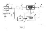
- Fig. 1 is a block diagram showing a general composition of a signal reproducing apparatus of the invention
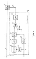
- Fig. 2 is a block diagram of a first embodiment of a signal reproducing apparatus of the invention
- Fig. 3 is a spectrum diagram of parts in Fig. 2,
- Fig. 4 is a block diagram showing a first embodiment of a detecting circuit
- Fig. 5 is a block diagram showing a second embodiment of a detecting circuit
- Fig. 6 is waveform diagram of parts in Fig. 5,
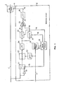
- Fig. 7 is a block diagram of a second embodiment of a signal reproducing apparatus of the invention.
- Fig. 8 is a spectrum diagram of parts in Fig. 7,
- Fig. 9 is a block diagram of a third embodiment of a signal reproducing apparatus of the invention.
- Fig. 10 is a spectrum diagram of parts in Fig. 9,
- Fig. 11 is a block diagram showing a first embodiment of frequency demodulation block
- Fig. 12 is a waveform diagram of parts in Fig. 11, and
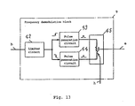
- Fig. 13 is a block diagram showing a second embodiment of frequency demodulation block.
- Fig. 1 shows a block diagram showing a general structure of a signal reproducing apparatus capable of removing cross modulation due to secondary distortion.
- a recording medium 100 is an optical disc, magnetic disc, magnetic tape or the like, which records a mixed signal of a first distortion wave having a video signal frequency-modulated at carrier frequency fc and a second modulation wave having an audio signal frequency-modulated in a frequency region (f1) lower than fc.
- a reproducing device 200 is, for example, an optical head or magnetic head, which reproduces the mixed signal from the recording medium 100, and obtains a reproduced FM signal.
- a reproduced FM signal a containing secondary distortion coming in from the reproducing device 200 through an input terminal 1 is passed through a high-pass filter (HPF) 7, and is frequency-demodulated in a frequency demodulation block 9, and a signal e is obtained.
- HPF high-pass filter
- a band-pass filter (BPF) 4 separates an audio modulation signal c from the signal a.
- a detecting circuit 6 accurately detects a cross modulation component f1 contained in the signal e by the output signal e of the frequency demodulation block 9 and the output signal c of the BPF 4, and controls the frequency demodulation block 9 by a signal h so as to minimize the residual component.
- the frequency modulation block 9 may enter the output of the BPF 4 (indicated by broken line), in addition to the outputs of the HPF 7 and detecting circuit 6.
- Fig. 2 shows a block diagram of a first embodiment of a signal reproducing apparatus capable of removing the cross modulation due to secondary distortion
- Fig. 3 shows a signal spectrum diagram corresponding to the parts in Fig. 2.
- the reproduced FM signal a containing secondary distortion coming in from the input terminal 1 is passed through the high-pass filter (HPF) 7, and is frequency-demodulated in a frequency demodulation circuit 2 in the frequency demodulation block 9 to obtain a signal b.
- the audio modulation signal c separated from the signal a by the band-pass filter (BPF) 4 is adjusted to an optimum gain in a gain adjusting circuit 5 by the output signal h from the detecting circuit 6 to obtain a signal d.
- BPF band-pass filter
- the detecting circuit 6 accurately detects the cross modulation component f1 contained in the signal e from the output signal c of the BPF 4 and the output signal e of the subtracting circuit 3, and creates a signal h for controlling the gain adjusting circuit 5.
- the frequency demodulation block 9 is composed of frequency demodulation circuit 2, gain adjusting circuit 5 and subtracting circuit 3.
- fc is the carrier frequency of FM video signal
- f1 is the frequency of audio modulation signal.
- FIG. 4 A constituent example of the detecting circuit 6 is shown in Fig. 4.
- the output of the BPF 11 for filtering the cross modulation frequency component f1 contained in the demodulated output signal e and the signal c which is the output of the BPF 4 are multiplied in a multiplier 10.
- the DC component of the output of the multiplier is positive, for example, if the signal c and signal e are in phase, negative if out of phase, and zero if there is no f1 component in signal e.
- the DC component is taken out by the LPF 12.
- the precision of detection may be outstandingly enhanced.
- the horizontal synchronous signal or vertical synchronous signal is separated in the synchronous separation circuit 14 by the demodulated signal e, and the output of the LPF 12 in the synchronous signal segment is held in a sample hold circuit (S/H) 13.
- the sample-held voltage is compared with a reference voltage Vref (for example, zero) in a comparator (COMP) 15, and depending on the difference, the output signal of the comparator 15 is delivered to the gain adjusting circuit 5 as signal h through the LPF 16 so as to increase or decrease the level of the gain adjusting circuit 5.
- Vref for example, zero
- the gain adjusting circuit 5 may be composed of a multiplier, for example. Or the gain adjusting circuit 5 may be controlled at the output level of the S/H 13, and in such a case, the comparator 15 and the LPF 16 may be omitted.
- FIG. 5 Another composition of detecting circuit is shown in Fig. 5.
- the output signal c of the BPF 4 is fed to an inverting circuit 20, and is also fed in a switch circuit 21.
- the signal c and the output signal of the inverting circuit are alternately changed over at intervals of one horizontal synchronizing period or one vertical synchronizing period, and the output is delivered to a multiplier 22.
- the output signal e of the subtracting circuit 3 is passed through a BPF 23 for filtering cross modulation component f1, and is sent into the multiplier 22. If the cross modulation component f1 is present in the output of the BPF 23, the DC output level of the multiplier 22 will possess a positive or negative step difference alternatively in every specified period. As the cross modulation component f1 becomes smaller, the DC step difference becomes also smaller, and when the cross modulation component is completely removed, the DC step difference becomes zero. Accordingly, the feedback control is effected so as to render this DC step difference zero.
- the DC component of the multiplier 22 is taken out in the LPF 24, and is alternately held in specified period in sample hold circuits (S/H) 25, 26.
- the potentials of the outputs of the sample hold circuit 25, 26 are compared in a comparator (COMP) 27, and a control signal is delivered.
- the control signal is delivered to the gain adjusting circuit 5 through a LPF 28.
- a timing generation circuit 30 generates a specified timing on the basis of a synchronous signal from a synchronous separation circuit 29. The waveforms of parts are shown in Fig. 6.
- the synchronous signal separation circuit 29 suppose the vertical synchronous signal is separated from signal e. It may be also a horizontal synchronous signal, which does not matter.
- the pulse P1 indicating this vertical synchronous signal
- pulses of P2, P3, P4 are generated in the timing generation circuit 30.
- the DC output level of the multiplier 22 produces a step difference in every period of P3, and it is signals P5, P6 that are obtained by holding alternately with pulses P3, P4.
- Signal P5 solid line
- P6 broken line
- Fig. 7 shows a block diagram of a second embodiment of a signal reproducing apparatus capable of removing cross modulation due to tertiary distortion of the invention
- Fig. 8 shows a signal spectrum diagram corresponding to the parts in Fig. 7.
- a reproduced FM signal a containing tertiary distortion coming in from an input terminal 1 is passed through a high-pass filter (HPF) 7, and frequency-demodulated in a frequency demodulation circuit 2 of a frequency demodulation block 9, and a signal b is obtained.
- the audio modulation signal separated from the signal a by a band-pass filter (BPF) 4 is doubled in frequency in a doubling circuit 8 to be signal c.
- the signal c is adjusted to an optimum gain in a gain adjusting circuit 5 depending on the information from a detecting circuit 6 to be a signal d.
- the signal d is subtracted from demodulated signal b in a subtracting circuit 3 to become an output demodulated signal e.
- the detecting circuit 6 is to accurately detect the cross modulation component 2f1 contained in the signal e from the output signal c of the doubling circuit 8 and the output signal e of the subtracting circuit 3, and to control the gain adjusting circuit 5.
- the doubling circuit 8 is composed of, for example, multiplier and band-pass filter.
- the composition of frequency demodulation block 9 and the composition and operation of detecting circuit 6 are as described above.
- Fig. 9 shows a block diagram of a third embodiment of the invention
- Fig. 10 shows signal spectra of parts in Fig. 9.
- a reproduced FM signal a containing secondary distortion coming in from an input terminal 1 is passed through a high-pass filter (HPF) 7 to be signal b, and is frequency-demodulated at carrier frequency fc in a frequency demodulation block 9 to be signal e.
- HPF high-pass filter
- a detecting circuit 6 feeds the audio modulation signal separated from the signal a in a band-pass filter (BPF) 4 and the output signal e of the frequency modulation block 9, accurately detects the cross modulation component f1 contained in the signal e, and controls the frequency demodulation block 9 at control signal h.
- the frequency demodulation block 9 comprises a differential input type limiter circuit 40 and a pulse counter circuit 41.
- the input signal b is compared with a reference potential ref to actuate the limiter, and generates a square wave having a duty ratio of 1:1 (Fig. 12, 1), 2)).
- a secondary distortion is generated, the square wave of duty ratio of 1:1 is not delivered, and cross modulation interference occurs at this time.
- This is shown in solid line ref1 in 3) and 4) in Fig. 12.
- the reference potential ref is changed to an optimum potential.
- the square wave with duty ratio of 1:1 is obtained as shown in Fig. 12, 5).
- the secondary distortion is eliminated, and generation of cross modulation interference may be suppressed.
- This reference potential ref is controlled by the control signal h which is the output of the detecting circuit 6.
- the reference potential ref may be fixed, and the control signal h from the detecting circuit 6 may be superposed on the input signal to compose the limiter action, instead.
- the control signal h is in reverse phase of the illustrated example.
- the frequency demodulation block 9 comprises a limiter circuit 42, a pulse generation circuit 43 for generating a pulse at a leading edge, a pulse generation circuit 44 for generating a pulse at a trailing edge, and an adder circuit 45 for varying the addition ratio of the output signals of the pulse generation circuits 43, 44.
- the duty ratio of the output of the limiter circuit 42 is no longer 1:1, and if outputs of the pulse generation circuits 43, 44 are merely added at 1:1, secondary distortion is generated.
- the duty imbalance generated in the limiter due to the secondary distortion is compensated by adjusting the addition ratio, that is, the mixing balance. At this time, generation of cross modulation interference due to secondary distortion is suppressed.
- the control signal h which is the output of the detecting circuit 6, the addition ratio of the adder circuit 45 is controlled.
- the composition and operation of the detecting circuit 6 are as shown in the foregoing embodiments in Figs. 4, 5, 6.
- phase adjusting circuit for adjusting the phase may be inserted before or after the gain adjusting circuit 5.
- the synchronous separation circuits 14, 29 may be replaced by circuits for detecting segments free from video signal.
- timing pulse from the timing generation circuit 30 may be variously considered in the method other than shown in the above embodiment, and, for example, a pair of P3, P4 pulses may be entered in one vertical synchronous signal segment, and the cross modulation component in the vertical synchronous signal segment may be detected.
- the inverting circuit 20 and switch circuit 21 may be inserted between the BPF 23 and multiplier 22, and the information of signal e may be inverted in every specified period.
- the second cross modulation component f1 is not limited to the audio FM signal, and various other signals may be considered, such as color difference FM signal, low region conversion color signal, pilot signal, and audio digital signal.
- the video signal of the first cross modulation wave includes, needless to say, brightness signal, color difference signal, high definition television signal, band compressed signal, etc.
Landscapes
- Engineering & Computer Science (AREA)
- Multimedia (AREA)
- Signal Processing (AREA)
- Power Engineering (AREA)
- Television Signal Processing For Recording (AREA)
Applications Claiming Priority (6)
| Application Number | Priority Date | Filing Date | Title |
|---|---|---|---|
| JP1326331A JPH03186089A (ja) | 1989-12-15 | 1989-12-15 | 信号再生装置 |
| JP326332/89 | 1989-12-15 | ||
| JP326331/89 | 1989-12-15 | ||
| JP1326332A JPH03186083A (ja) | 1989-12-15 | 1989-12-15 | 信号再生装置 |
| JP2148274A JPH0440183A (ja) | 1990-06-05 | 1990-06-05 | 信号再生装置 |
| JP148274/90 | 1990-06-05 |
Publications (2)
| Publication Number | Publication Date |
|---|---|
| EP0433032A2 true EP0433032A2 (fr) | 1991-06-19 |
| EP0433032A3 EP0433032A3 (en) | 1992-08-05 |
Family
ID=27319525
Family Applications (1)
| Application Number | Title | Priority Date | Filing Date |
|---|---|---|---|
| EP19900313473 Withdrawn EP0433032A3 (en) | 1989-12-15 | 1990-12-11 | Signal reproducing apparatus |
Country Status (2)
| Country | Link |
|---|---|
| US (1) | US5218448A (fr) |
| EP (1) | EP0433032A3 (fr) |
Cited By (2)
| Publication number | Priority date | Publication date | Assignee | Title |
|---|---|---|---|---|
| EP0577419A3 (en) * | 1992-07-03 | 1994-07-27 | Sony Corp | Signal demodulating apparatus for a reproduced video signal |
| FR2821500A1 (fr) * | 2001-02-26 | 2002-08-30 | St Microelectronics Sa | Procede et dispositif de compensation du decalage cc dynamique d'un recepteur a conversion directe |
Families Citing this family (6)
| Publication number | Priority date | Publication date | Assignee | Title |
|---|---|---|---|---|
| JP3117608B2 (ja) * | 1994-02-10 | 2000-12-18 | シャープ株式会社 | 受信装置 |
| US6011765A (en) * | 1996-04-12 | 2000-01-04 | Sony Corporation | Recording medium having copying protection signals recorded in superposition on main signals |
| KR100256251B1 (ko) * | 1997-06-30 | 2000-05-15 | 김영환 | 이중 샘플링 아날로그 저역 통과 필터 |
| US6393596B1 (en) * | 1998-10-30 | 2002-05-21 | Hewlett-Packard Company | Missing pulse detector using synchronous detection |
| EP1316092B1 (fr) * | 2000-08-03 | 2010-07-14 | Broadcom Corporation | Circuit et procede d'alignement multiphase |
| WO2017174116A1 (fr) * | 2016-04-05 | 2017-10-12 | Telefonaktiebolaget Lm Ericsson (Publ) | Suppression d'interférence dans un dispositif émetteur-récepteur radio |
Family Cites Families (13)
| Publication number | Priority date | Publication date | Assignee | Title |
|---|---|---|---|---|
| JPS5437528A (en) * | 1977-08-30 | 1979-03-20 | Sony Corp | Processing circuit for video signal |
| US4322746A (en) * | 1978-10-06 | 1982-03-30 | Hitachi, Ltd. | Crosstalk attenuator system |
| DE2850514C2 (de) * | 1978-11-22 | 1980-11-27 | Institut Fuer Rundfunktechnik Gmbh, 8000 Muenchen | Regelschaltung für FM-Demodulatoren |
| JPS57189311A (en) * | 1981-05-14 | 1982-11-20 | Olympus Optical Co Ltd | Fm demodulating system |
| JPS58203605A (ja) * | 1982-05-20 | 1983-11-28 | Pioneer Video Kk | 多重記録情報の再生装置 |
| JPS5929992A (ja) * | 1982-08-13 | 1984-02-17 | Hitachi Ltd | 積層型熱交換器 |
| US4561113A (en) * | 1983-04-09 | 1985-12-24 | Trio Kabushiki Kaisha | Distortion canceller for FM receiver |
| JPS6051388A (ja) * | 1983-08-31 | 1985-03-22 | Sony Corp | 記録再生装置の二次ビートキャンセル回路 |
| US4878128A (en) * | 1986-05-12 | 1989-10-31 | Canon Kabushiki Kaisha | Video signal reproducing apparatus |
| DE277000T1 (de) * | 1987-01-27 | 1988-11-24 | Victor Company Of Japan, Ltd., Yokohama, Kanagawa | Geraet zur magnetischen aufzeichnung und/oder wiedergabe. |
| EP0300801B1 (fr) * | 1987-07-21 | 1995-02-22 | Matsushita Electric Industrial Co., Ltd. | Appareil de démodulation de fréquence |
| US4908581A (en) * | 1988-07-21 | 1990-03-13 | Matsushita Electric Industrial Co., Ltd. | Frequency demodulator having circuit cancelling undesired signal components |
| JPH083939B2 (ja) * | 1988-09-19 | 1996-01-17 | 松下電器産業株式会社 | Fm復調回路 |
-
1990
- 1990-12-11 EP EP19900313473 patent/EP0433032A3/en not_active Withdrawn
- 1990-12-12 US US07/626,298 patent/US5218448A/en not_active Expired - Fee Related
Cited By (4)
| Publication number | Priority date | Publication date | Assignee | Title |
|---|---|---|---|---|
| EP0577419A3 (en) * | 1992-07-03 | 1994-07-27 | Sony Corp | Signal demodulating apparatus for a reproduced video signal |
| US5493346A (en) * | 1992-07-03 | 1996-02-20 | Sony Corporation | Signal demodulating apparatus capable of effectively suppressing the beat interference caused by the pilot signal |
| FR2821500A1 (fr) * | 2001-02-26 | 2002-08-30 | St Microelectronics Sa | Procede et dispositif de compensation du decalage cc dynamique d'un recepteur a conversion directe |
| EP1235355A3 (fr) * | 2001-02-26 | 2002-09-18 | STMicroelectronics S.A. | Procédé et dispositif de compensation du décalage CC dynamique d'un récepteur à conversion directe |
Also Published As
| Publication number | Publication date |
|---|---|
| EP0433032A3 (en) | 1992-08-05 |
| US5218448A (en) | 1993-06-08 |
Similar Documents
| Publication | Publication Date | Title |
|---|---|---|
| EP0730375A2 (fr) | Appareil d'enregistrement et de reproduction magnétique | |
| US5218448A (en) | Signal reproducing apparatus | |
| US4208674A (en) | Time base error correcting apparatus | |
| PL108985B1 (en) | Apparatus for reproducing colour images | |
| KR930006540B1 (ko) | 콤필터 억제 회로를 갖는 광대역 vcr | |
| EP0073468B1 (fr) | Système compensateur pour manque de signal | |
| JPH0440183A (ja) | 信号再生装置 | |
| EP0161810B1 (fr) | Appareil de traitement de signaux de chrominance | |
| JP3325469B2 (ja) | 自動利得制御ループ回路 | |
| EP0289346B1 (fr) | Circuit démodulateur de fréquence | |
| GB2103906A (en) | Time axis correction device for multiplex information-carrying signal obtained from recording medium | |
| KR940003664B1 (ko) | 디지틀 신호 검출장치 | |
| US4334249A (en) | Apparatus for use in recording a pulse signal on a magnetic recording medium | |
| US5598274A (en) | Image signal recording and reproducing system | |
| KR940004511B1 (ko) | 브이씨알의 재생 색신호 자동 보정 시스템 | |
| EP0456501B1 (fr) | Circuit d'élimination de signal pilote | |
| KR900000335B1 (ko) | 영상신호 재생장치 | |
| JPS6221435B2 (fr) | ||
| JPS61158283A (ja) | 時間軸補正装置 | |
| JPH03186089A (ja) | 信号再生装置 | |
| KR900004957B1 (ko) | 반송 색신호의 기록 재생 장치 | |
| JP2659464B2 (ja) | 磁気記録再生装置 | |
| US4583130A (en) | AST for a two track VTR | |
| JPH0625103Y2 (ja) | 外部リセット機能付きfm変調回路 | |
| EP0300801A2 (fr) | Appareil de démodulation de fréquence |
Legal Events
| Date | Code | Title | Description |
|---|---|---|---|
| PUAI | Public reference made under article 153(3) epc to a published international application that has entered the european phase |
Free format text: ORIGINAL CODE: 0009012 |
|
| AK | Designated contracting states |
Kind code of ref document: A2 Designated state(s): DE FR GB NL |
|
| PUAL | Search report despatched |
Free format text: ORIGINAL CODE: 0009013 |
|
| AK | Designated contracting states |
Kind code of ref document: A3 Designated state(s): DE FR GB NL |
|
| 17P | Request for examination filed |
Effective date: 19930128 |
|
| 17Q | First examination report despatched |
Effective date: 19941220 |
|
| STAA | Information on the status of an ep patent application or granted ep patent |
Free format text: STATUS: THE APPLICATION IS DEEMED TO BE WITHDRAWN |
|
| 18D | Application deemed to be withdrawn |
Effective date: 19950421 |