EP0433488A1 - Steuerschaltung für einen Leistungswandler - Google Patents
Steuerschaltung für einen Leistungswandler Download PDFInfo
- Publication number
- EP0433488A1 EP0433488A1 EP89123756A EP89123756A EP0433488A1 EP 0433488 A1 EP0433488 A1 EP 0433488A1 EP 89123756 A EP89123756 A EP 89123756A EP 89123756 A EP89123756 A EP 89123756A EP 0433488 A1 EP0433488 A1 EP 0433488A1
- Authority
- EP
- European Patent Office
- Prior art keywords
- switch
- transformer
- winding
- power transformer
- power
- Prior art date
- Legal status (The legal status is an assumption and is not a legal conclusion. Google has not performed a legal analysis and makes no representation as to the accuracy of the status listed.)
- Withdrawn
Links
Images
Classifications
-
- H—ELECTRICITY
- H02—GENERATION; CONVERSION OR DISTRIBUTION OF ELECTRIC POWER
- H02M—APPARATUS FOR CONVERSION BETWEEN AC AND AC, BETWEEN AC AND DC, OR BETWEEN DC AND DC, AND FOR USE WITH MAINS OR SIMILAR POWER SUPPLY SYSTEMS; CONVERSION OF DC OR AC INPUT POWER INTO SURGE OUTPUT POWER; CONTROL OR REGULATION THEREOF
- H02M3/00—Conversion of DC power input into DC power output
- H02M3/22—Conversion of DC power input into DC power output with intermediate conversion into AC
- H02M3/24—Conversion of DC power input into DC power output with intermediate conversion into AC by static converters
- H02M3/28—Conversion of DC power input into DC power output with intermediate conversion into AC by static converters using discharge tubes with control electrode or semiconductor devices with control electrode to produce the intermediate AC
- H02M3/325—Conversion of DC power input into DC power output with intermediate conversion into AC by static converters using discharge tubes with control electrode or semiconductor devices with control electrode to produce the intermediate AC using devices of a triode or a transistor type requiring continuous application of a control signal
- H02M3/335—Conversion of DC power input into DC power output with intermediate conversion into AC by static converters using discharge tubes with control electrode or semiconductor devices with control electrode to produce the intermediate AC using devices of a triode or a transistor type requiring continuous application of a control signal using semiconductor devices only
- H02M3/33538—Conversion of DC power input into DC power output with intermediate conversion into AC by static converters using discharge tubes with control electrode or semiconductor devices with control electrode to produce the intermediate AC using devices of a triode or a transistor type requiring continuous application of a control signal using semiconductor devices only of the forward type
- H02M3/33546—Conversion of DC power input into DC power output with intermediate conversion into AC by static converters using discharge tubes with control electrode or semiconductor devices with control electrode to produce the intermediate AC using devices of a triode or a transistor type requiring continuous application of a control signal using semiconductor devices only of the forward type with automatic control of the output voltage or current
- H02M3/33553—Conversion of DC power input into DC power output with intermediate conversion into AC by static converters using discharge tubes with control electrode or semiconductor devices with control electrode to produce the intermediate AC using devices of a triode or a transistor type requiring continuous application of a control signal using semiconductor devices only of the forward type with automatic control of the output voltage or current with galvanic isolation between input and output of both the power stage and the feedback loop
Definitions
- This invention relates to power systems and devices, and more particularly to a control circuit for controlling the duty cycle of a power converter.
- Control circuits are utilized for controlling the duty cycle of a power transformer within a magnetic power converter system.
- the on time and off time of a power switch which controls energization of the primary winding of the power transformer within the system may be controlled by integrated circuitry using external references which detect variations across the load of the system in order to maintain the output voltage constant.
- control circuits require isolating elements, for example, optical couplers in order to couple the output on the secondary side of the transformer to the primary side.
- Such circuitry is costly and requires numerous circuit elements in order to perform the control operation.
- a control circuit for a power converter which includes a power transformer having a primary transformer winding for receiving an input voltage signal and a secondary transformer winding for generating an output signal is provided.
- the control of the on and off time of the power switch which in turn determines the on and off time of the power transformer, is accomplished utilizing a control transformer having a plurality of windings.
- a switch is provided which is coupled to the control transformer. The switch is conductive to render the power transformer on and when non-conducting renders the power transformer off. The state of the switch is controlled through magnetic coupling between the windings of the control transformer to thereby render the output voltage derived from the power transformer constant while the switch on time remains constant and the switch off time is variable.
- the on time of the switch which is coupled to the control transformer is also variable utilizing a feed forward circuit.
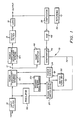
- Control circuit 10 is utilized for controlling the duty cycle of a power switch and transformer, generally identified by the numeral 12 having a primary winding 12a and a secondary winding l2b.
- Power transformer 12 receives an input signal via an input filter 14, and generates an output signal to a load 16 via an output filter 18.
- the duty cycle of power transformer 12 is controlled by the operation of a power switch 24 which is coupled to power transformer primary winding 12a.
- the energization and de-energization of power switch 24 is controlled by pulse width switch drive circuitry 26 which will be further described with respect to Figure 2.
- Pulse width switch drive circuitry 26 includes a plurality of switches and a control transformer which is responsive to the output voltage of power transformer 12 in order to maintain the output voltage of power transformer 12 constant. Unlike previously developed control circuits, the present invention does not utilize any internal or external timing elements for controlling the duty cycle of the power transformer in the power converter system.
- Pulse width switch drive circuitry 26 receives a feedback signal via signal line 32 which is developed from the output of power transformer secondary winding 12b.
- the output signal of power transformer 12 is applied to a comparator 36 which also receives a reference voltage level from reference 38.
- the output of comparator 36 is applied to an amplifier 42 whose output is applied to a comparator 46.
- Comparator 46 also receives a reference output voltage from a ramp generator 48 which includes an additional power transformer secondary winding 12c ( Figure 2) of power transformer 12.
- comparator 46 When present, the output of comparator 46 provides a feedback signal via signal line 32 to pulse width switch drive circuitry 26 which in turn activates a switch within switch turn off circuitry 30 to turn on power switch 24 and therefore terminate the off time of the duty cycle of the signal applied to power transformer 12.
- the input signal is applied to pulse width switch drive circuitry 26 through a voltage regulator 50.
- An additional aspect of the present invention is the control of the on time of power switch 24. Control of the on time of power switch 24 is variable through the use of an additional primary winding 12d of power transformer 12 to supply a feed forward signal to pulse width switch drive circuitry 26.
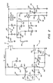
- power transformer 12 includes primary windings 12a and 12d, and secondary windings 12b and 12c.
- the system input voltage is applied to power transformer primary winding 12a and the output voltage is generated from power transformer secondary winding 12b.
- Interconnected to power transformer secondary winding 12b is a diode 60 whose output is connected to output filter 18.
- Output filter 18 includes an inductor 62, a diode 64 and a capacitor 66.
- Pulse width switch drive circuitry 26 includes a control transformer 70 having windings 70a, 70b, 70C, and 70d.
- Pulse width switch drive circuitry 26 and switch turn off circuit 30 further includes four switches in the form of transistors 80, 82, 84, and 86.
- Power switch 24 may comprise, for example, a field effect transistor 88.
- the input voltage signal is applied to control transformer winding 70a through a resistor 90 and to the base of transistor 80 through a resistor 92.
- the emitter of transistor 80 is interconnected to a resistor 94 which is connected to primary winding 12d of power transformer 12.
- the emitter of transistor 80 is also interconnected to winding 70b of control transformer 70 via a diode 96 and parallel connected capacitor 98.
- the base of transistor 82 is interconnected to winding 70c of control transformer 70 via a resistor 100.
- the base of transistor 84 is interconnected to resistors 102 and 104.
- Reference voltage source 38 may comprise, for example, a programmable zener diode 106, the cathode of which is connected to the emitter of transistor 86.
- the input of programmable zener 106 is connected to resistors 108 and 110 which receive the output voltage signal from power transformer secondary winding 12b.
- Power transformer secondary winding 12c is interconnected to the base of transistor 86 via a diode 112 and a resistor 114, a capacitor 116 and a resistor 118. Power transformer secondary winding 12c is interconnected to winding 70d of control transformer 70 via a diode 122 and capacitor 124. The output of power transformer secondary winding 12c is also applied to the emitter of transistor 86 via a resistor 130.
- control transformer 70 and transistors 80, 82, 84, 86 and switch field effect transistor 88 The input voltage applied to pulse width switch drive circuitry 26 and more specifically through resistors 90 and 92 initially caused transistor 80 to turn on.
- transistor 80 When transistor 80 is on, transistor 82 is off because of the reverse polarity of the voltage across winding 70c at the base of transistor 82.
- Transistor 80 is latched on and is self-driven by the current feedback in control transformer 70. Current flows through resistor 94 and into the gate of field effect transistor 88 turning field effect transistor 88 on.
- the base current flowing to transistor 80 begins to decrease as the transformer exciting current 1 L shown in Figure 2 flowing through an inductor 70b′ for illustrative purposes only, it being understood that inductor 70b′ is not an actual circuit component but is the exciting inductance of control transformer 70.
- transistor 80 regeneratively turns off.
- the inductive kick back of control transformer 70 and particularly winding 70c rapidly turns transistor 82 on to discharge the gate-source capacitance of field effect transistor 88 which very rapidly turns field effect transistor 88 off.
- the turn off of field effect transistor 88 is initiated when the current flowing within inductor 70b′ is equal to the current within winding 70b of control transformer 70 such that the current I B is equal to zero.
- the voltage across inductor 70b′ is constant and is equal to the diode drop across diode 96 plus the base-emitter voltage drop across transistor 80. Therefore, the current I L . is a ramp function.
- the current flowing within winding 70b of control transformer 70 is constant after field effect transistor 88 turns on and is determined by the value of resistor 94 and the voltage across this resistor.
- the on time of field effect transistor 88, the pulse width is then determined by the values of inductance 70b′, resistor 94, the turns ratio between windings 70a and 70b, the voltage across resistor 94, the base-emitter drop of transistor 80 and the voltage drop across diode 96. If any of these parameters or voltages are caused to vary, the pulse width of the activation pulse applied to power transformer primary winding 12a will vary accordingly.
- Programmable zener 106 sets a voltage level that is dependent on the output voltage of power transformer secondary winding 12b. Programmable zener 106 functions as a reference voltage and error amplifier.
- field effect transistor 88 When field effect transistor 88 is turned on, secondary winding 12c of power transformer 12 charges capacitor 116 to a value of the ratio of the turns between secondary winding 12c and primary winding 12a of power transformer 12 multiplied by the input voltage applied to primary winding 12a.
- the charged voltage level of capacitor 116 is higher than the voltage at the emitter of transistor 86 and therefore transistors 86 and 84 are turned off.
- the voltage on the base of transistor 86 begins to decrease as capacitor 116 discharges through resistor 118. When this voltage level drops lower than the voltage level appearing at the emitter of transistor 86, transistor 86 turns on which in turn turns on transistor 84. Transistor 84 then pulses winding 70d of control transformer 70 which pulse is magnetically coupled to winding 70b thereby turning on transistor 80. When transistor 80 is on, as previously stated, field effect transistor 88 is turned on, thereby terminating the off period of field effect transistor 88. This off time is regulated in order to maintain the output voltage of power transformer 12 constant. Variations in the output voltage is determinative of when transistor 84 will conduct in order to pulse winding 70d which in turn actuates transistor 80.
- the ramp generator 48 ( Figure 1) function is performed by capacitor 116 and resistor 118. Comparator 46 function is performed by transistor 86.
- Switch turn off circuitry 30 ( Figure 1) includes transistor 84 and winding 70d of control transformer 74.
- Control circuit 10 thereby generates a feedback pulse, magnetically induced, from winding 70d of control transformer 70 to winding 70b of control transformer 70 to thereby terminate the off period of power transformer 12.
- Variations in the on time of power transformer 12 are accomplished by the present control circuit 10 by sensing variations in the input voltage through power transformer primary winding 12d.
- the induced voltage of winding 12d effects the current flowing through resistor 94 which effects the on time of field effect transistor 88.
- ramp generator 48 ( Figure 1) has been shown as comprising capacitor 116 and resistor 118 in combination with secondary winding 12c of power transformer 12, other internal voltage references may be utilized with the present invention for generating a reference voltage level for operation of transistor 86.
- the present invention provides for a magnetically controlled control circuit for a power transformer. Changes in the output voltage are sensed, and through magnetic coupling, the off time of the power transformer primary winding is controlled.
- the present invention therefore provides for a control circuit which is simple in operation, reliable and cost effective.
Landscapes
- Engineering & Computer Science (AREA)
- Power Engineering (AREA)
- Dc-Dc Converters (AREA)
Applications Claiming Priority (1)
| Application Number | Priority Date | Filing Date | Title |
|---|---|---|---|
| US07/283,153 US4926303A (en) | 1988-12-12 | 1988-12-12 | Control circuit for a switching DC to DC Power converter including a multi-turn control transformer |
Publications (1)
| Publication Number | Publication Date |
|---|---|
| EP0433488A1 true EP0433488A1 (de) | 1991-06-26 |
Family
ID=23084762
Family Applications (1)
| Application Number | Title | Priority Date | Filing Date |
|---|---|---|---|
| EP89123756A Withdrawn EP0433488A1 (de) | 1988-12-12 | 1989-12-22 | Steuerschaltung für einen Leistungswandler |
Country Status (2)
| Country | Link |
|---|---|
| US (1) | US4926303A (de) |
| EP (1) | EP0433488A1 (de) |
Cited By (1)
| Publication number | Priority date | Publication date | Assignee | Title |
|---|---|---|---|---|
| CN102570820A (zh) * | 2010-12-20 | 2012-07-11 | 凹凸电子(武汉)有限公司 | Dc/dc变换器、控制变压器的方法及电源变换系统 |
Families Citing this family (12)
| Publication number | Priority date | Publication date | Assignee | Title |
|---|---|---|---|---|
| US4926303A (en) * | 1988-12-12 | 1990-05-15 | Qualitron, Inc. | Control circuit for a switching DC to DC Power converter including a multi-turn control transformer |
| US5448469A (en) * | 1990-02-15 | 1995-09-05 | Deutsche Thomson-Brandt Gmbh | Switch mode power supply with output feedback isolation |
| FR2662557B1 (fr) * | 1990-05-22 | 1997-07-25 | Thomson Brandt Armements | Convertisseur basse tension-haute tension. |
| US5162663A (en) * | 1990-09-28 | 1992-11-10 | Ncr Corporation | Selective output disconnect for a single transformer converter |
| US5392206A (en) * | 1993-02-12 | 1995-02-21 | Valor Electronics, Inc. | Control circuit for a switching DC-DC power converter including a controlled magnetic core flux resetting technique for output regulation |
| US5499176A (en) * | 1993-08-12 | 1996-03-12 | Toko America, Inc. | Pulse transformer circuit for isolating electrical signals |
| US7269034B2 (en) | 1997-01-24 | 2007-09-11 | Synqor, Inc. | High efficiency power converter |
| EP0954899A2 (de) | 1997-01-24 | 1999-11-10 | Fische, LLC | Hocheffizienter stromrichter |
| JP3492882B2 (ja) * | 1997-04-07 | 2004-02-03 | パイオニア株式会社 | スイッチング電源装置 |
| DE19855615A1 (de) * | 1997-12-03 | 1999-06-10 | Fuji Electric Co Ltd | Schaltnetzteil |
| US7911817B2 (en) * | 2008-09-18 | 2011-03-22 | Dell Products L.P. | Systems and methods for controlling energy consumption of AC-DC adapters |
| US10199950B1 (en) | 2013-07-02 | 2019-02-05 | Vlt, Inc. | Power distribution architecture with series-connected bus converter |
Citations (4)
| Publication number | Priority date | Publication date | Assignee | Title |
|---|---|---|---|---|
| US3541420A (en) * | 1968-03-27 | 1970-11-17 | Motorola Inc | Voltage converter and regulator |
| US3924172A (en) * | 1974-07-11 | 1975-12-02 | Honeywell Inf Systems | Power supply |
| US4323961A (en) * | 1980-09-12 | 1982-04-06 | Astec Components, Ltd. | Free-running flyback DC power supply |
| US4926303A (en) * | 1988-12-12 | 1990-05-15 | Qualitron, Inc. | Control circuit for a switching DC to DC Power converter including a multi-turn control transformer |
Family Cites Families (4)
| Publication number | Priority date | Publication date | Assignee | Title |
|---|---|---|---|---|
| US3134940A (en) * | 1961-12-29 | 1964-05-26 | Bell Telephone Labor Inc | Regulated voltage converter circuit |
| US4347559A (en) * | 1981-03-02 | 1982-08-31 | Texas Instruments Incorporated | Switching power supply |
| FR2560697B3 (fr) * | 1984-03-02 | 1986-07-04 | Rv Const Electriques | Circuit de regulation d'alimentation stabilisee a decoupage |
| IT1188718B (it) * | 1986-05-22 | 1988-01-28 | Neywell Information Systems It | Alimentatore a commutazione |
-
1988
- 1988-12-12 US US07/283,153 patent/US4926303A/en not_active Expired - Fee Related
-
1989
- 1989-12-22 EP EP89123756A patent/EP0433488A1/de not_active Withdrawn
Patent Citations (4)
| Publication number | Priority date | Publication date | Assignee | Title |
|---|---|---|---|---|
| US3541420A (en) * | 1968-03-27 | 1970-11-17 | Motorola Inc | Voltage converter and regulator |
| US3924172A (en) * | 1974-07-11 | 1975-12-02 | Honeywell Inf Systems | Power supply |
| US4323961A (en) * | 1980-09-12 | 1982-04-06 | Astec Components, Ltd. | Free-running flyback DC power supply |
| US4926303A (en) * | 1988-12-12 | 1990-05-15 | Qualitron, Inc. | Control circuit for a switching DC to DC Power converter including a multi-turn control transformer |
Cited By (1)
| Publication number | Priority date | Publication date | Assignee | Title |
|---|---|---|---|---|
| CN102570820A (zh) * | 2010-12-20 | 2012-07-11 | 凹凸电子(武汉)有限公司 | Dc/dc变换器、控制变压器的方法及电源变换系统 |
Also Published As
| Publication number | Publication date |
|---|---|
| US4926303A (en) | 1990-05-15 |
Similar Documents
| Publication | Publication Date | Title |
|---|---|---|
| US5963438A (en) | Bi-directional magnetic isolator | |
| EP0123030B1 (de) | Schaltnetzteil mit isolierter Rückkopplung | |
| US4967309A (en) | Dual current sensing driver circuit | |
| US4926303A (en) | Control circuit for a switching DC to DC Power converter including a multi-turn control transformer | |
| US3541420A (en) | Voltage converter and regulator | |
| US4774624A (en) | Boost voltage power supply for vehicle control system | |
| US4763236A (en) | DC-DC converter | |
| KR880700523A (ko) | 잡음 면역성 전류 감지 장치 부착 전원공급기 | |
| US4295083A (en) | Pulsed energy stepping motor power control unit | |
| WO1992018922A1 (en) | Switching regulator power supply with multiple isolated outputs | |
| JPH0655031B2 (ja) | フライバックスイッチングレギュレ−タ電源 | |
| US5557494A (en) | Drive circuit of an electromagnetic device | |
| EP0124210B1 (de) | Energieversorgung mit stromgesteuertem Sperrwandler | |
| US20020041478A1 (en) | Circuit for driving a solenoid | |
| US7151328B2 (en) | Auxiliary power source and method for operating the auxiliary power source, as well as circuit arrangement for switching a load | |
| US4349752A (en) | Magnetic couple drive circuit for power switching device | |
| EP0590223B1 (de) | Verfahren und Vorrichtung zur Energierückgewinnung bei der Ansteuerung induktiver Lasten | |
| EP1050953B1 (de) | Bei Nullspannung schaltendes Leistungsschaltnetzteil | |
| GB1139356A (en) | Voltage regulator circuit | |
| US3855518A (en) | Switching regulator using gate-turn-off scr | |
| US4266268A (en) | Switching power supply having energy storage inductor in primary circuit of output transformer | |
| EP0067174B1 (de) | Rückgekoppelter stromzuführungsverstärkerkreis | |
| JPS6249967B2 (de) | ||
| JPH08331839A (ja) | 電源回路 | |
| US4744020A (en) | Switching mode power supply |
Legal Events
| Date | Code | Title | Description |
|---|---|---|---|
| PUAI | Public reference made under article 153(3) epc to a published international application that has entered the european phase |
Free format text: ORIGINAL CODE: 0009012 |
|
| AK | Designated contracting states |
Kind code of ref document: A1 Designated state(s): AT BE CH DE ES FR GB GR IT LI LU NL SE |
|
| RBV | Designated contracting states (corrected) |
Designated state(s): DE FR GB IT |
|
| 17P | Request for examination filed |
Effective date: 19911127 |
|
| 17Q | First examination report despatched |
Effective date: 19930518 |
|
| STAA | Information on the status of an ep patent application or granted ep patent |
Free format text: STATUS: THE APPLICATION HAS BEEN WITHDRAWN |
|
| 18W | Application withdrawn |
Withdrawal date: 19940301 |
|
| R18W | Application withdrawn (corrected) |
Effective date: 19940301 |