EP0433520B1 - Mémoire de tampon élastique configurable pour le stockage transitoire de données asynchrones - Google Patents
Mémoire de tampon élastique configurable pour le stockage transitoire de données asynchrones Download PDFInfo
- Publication number
- EP0433520B1 EP0433520B1 EP89480187A EP89480187A EP0433520B1 EP 0433520 B1 EP0433520 B1 EP 0433520B1 EP 89480187 A EP89480187 A EP 89480187A EP 89480187 A EP89480187 A EP 89480187A EP 0433520 B1 EP0433520 B1 EP 0433520B1
- Authority
- EP
- European Patent Office
- Prior art keywords
- move
- data
- sector
- buffer
- bus
- Prior art date
- Legal status (The legal status is an assumption and is not a legal conclusion. Google has not performed a legal analysis and makes no representation as to the accuracy of the status listed.)
- Expired - Lifetime
Links
Images


Classifications
-
- G—PHYSICS
- G06—COMPUTING OR CALCULATING; COUNTING
- G06F—ELECTRIC DIGITAL DATA PROCESSING
- G06F5/00—Methods or arrangements for data conversion without changing the order or content of the data handled
- G06F5/06—Methods or arrangements for data conversion without changing the order or content of the data handled for changing the speed of data flow, i.e. speed regularising or timing, e.g. delay lines, FIFO buffers; over- or underrun control therefor
- G06F5/16—Multiplexed systems, i.e. using two or more similar devices which are alternately accessed for enqueue and dequeue operations, e.g. ping-pong buffers
-
- G—PHYSICS
- G06—COMPUTING OR CALCULATING; COUNTING
- G06F—ELECTRIC DIGITAL DATA PROCESSING
- G06F13/00—Interconnection of, or transfer of information or other signals between, memories, input/output devices or central processing units
- G06F13/38—Information transfer, e.g. on bus
- G06F13/40—Bus structure
- G06F13/4004—Coupling between buses
- G06F13/4027—Coupling between buses using bus bridges
- G06F13/405—Coupling between buses using bus bridges where the bridge performs a synchronising function
- G06F13/4059—Coupling between buses using bus bridges where the bridge performs a synchronising function where the synchronisation uses buffers, e.g. for speed matching between buses
-
- G—PHYSICS
- G06—COMPUTING OR CALCULATING; COUNTING
- G06F—ELECTRIC DIGITAL DATA PROCESSING
- G06F2205/00—Indexing scheme relating to group G06F5/00; Methods or arrangements for data conversion without changing the order or content of the data handled
- G06F2205/06—Indexing scheme relating to groups G06F5/06 - G06F5/16
- G06F2205/063—Dynamically variable buffer size
Definitions
- the present invention relates to an elastic buffer to be used for example in asynchronous communication systems, where transmitters and receivers working asynchronously, need to be synchronized, at least over periods corresponding to the time necessary for transmission of a unit of data.
- TDM time division multiplex
- random access memories are used.
- the technique is to write the input data into the random access memory using the received clock to operate a sequential address counter.
- the memory is read out by addressing it through a counter operated by the local or output clock. While the data is being read out, the new received data must be stored in a different memory chip because a memory cannot be written into and read from simultaneously. This method therefore requires a multiplicity of memory chips, and the arrangement overflows when both input and output address counters attempt to access the same memory chip.
- an elastic buffer as the one described in US-P-4 056 851 which includes a single random access memory from which information bits are read out at a rate determined by an output clock, and into which received information bits are written at a rate determined by an input clock, where the two clocks are not exactly synchronous.
- Timing and storage means are provided to accommodate the zero, one or two information bits, which may be received for storage in the memory, in the interval between the readout of two successive information bits from the memory. An alarm is given if the input and output clock rates are such that the memory is emptied, or is filled and about to overflow.
- the elastic buffer described in the above cited patent even if it provides an interesting alternative to the conventional first-in-first-out (FIFO) buffers, does not solve several supplementary problems.
- the provision for a buffering RAM is not enough to avoid the necessity for substantial external data and clock buffering, using registers.
- the elasticity between the two asynchronous data flows is limited to one or two bits, which excludes the possibility of asynchronous transmission and buffering of several bytes of data.
- the reception of data by the elastic buffer, and the retransmission of data remain two successive and alternating operations of a FLIP-FLOP type, which, in view of the limited capacity of the elastic buffer, affects the throughput of the buffer, and consequently, of the data transmission between the asynchronous emitter and receiver.
- US-A-4 175 287 discloses an elastic buffer implemented by a memory device divided into sections with control means for preventing that read and write operations occur in the same section.
- an object of the invention to provide an elastic buffer capable of simultaneously receiving and transmitting asynchronous data units covering several bytes of information, the data being, of course, transmitted in the order of their arrival.
- the mode of the sectors is set through the binary value affected to the delimiting flags, and the adequate chronology of the received/ transmitted data units is ensured by the rotation of the flag values throughout the RAM memory space.
- Fig. 1 is a schematic view of a data communication system wherein the elastic buffer of the invention may be used.
- Fig. 2 is a schematic view of the structure of a communication pico-processor shown in Fig. 1 and incorporating the elastic buffer according to the invention.
- Fig. 3 is a schematic view of the elastic buffer and of its principle of operation.
- Fig. 4 is a schematic view of another organization of the buffer of Fig.3.
- Fig. 5A is the schematic representation of an implementation of the elastic buffer and the associated logic.
- Fig. 5B is a more detailed view of the mark flag register and associated logic, shown in Fig. 5A, in the case of a reconfigurable elastic buffer.
- Fig. 5C is a view of the logic for generating a "data move buffer full" signal, using the mark flag register of Fig. 5B.
- Fig. 5D is a view of the logic for generating a "data move buffer empty" signal, using the mark flag register of Fig. 5B.
- Fig. 6 and 7 are timing diagrams relevant to the operation of moving data into the elastic buffer.
- Fig. 8 and 9 are timing diagrams relevant to the operation of moving data out of the elastic buffer.
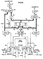
- FIG. 1 shows the configuration of a system (1) in which the present invention finds an exemplative and not limitative application.
- the system (1) is a communication system in which multiple users (not shown) are connected, through lines (24), to a line interface module LIM (7), and further to a shared memory, or packet memory PM (3), through an interconnection network NW (5).
- Such an arrangement is used, for instance, in communications controllers, and is more fully described in a copending patent application No. 88480102.8 filed on December 23th, 1988 by same applicant, entitled "Shared intelligent memory for the interconnection of distributed micro-processors".
- the shared memory (3) includes one or several memory banks (9) which can be acceded to through a memory bus (26).
- a pico-processor (11) provides for adaptation between the data/command words on said memory bus (26) and a Packet Memory Interface bus (PMI bus) (22) connected to the interconnection network (5).
- the interconnection network is a multiple port packet switch which, in response to data packets entered at one of its ports, can route said data packets to the required output port, through the packet memory (3).
- FIG. 1 A brief explanation of the system shown in Figure 1 should make understandable the interest for an elastic buffer according to the invention.
- a user connected to the packet memory (3) through a line (24) and a line interface module LIM (7) wants to write information into the packet memory, it transmits a request to the server (17) through an interface adapter IFA (19).
- the server (17) posts a control word corresponding to said request, into the local memory (15) of the LIM (7).
- a pico-processor (PP) (13) handles the control word stored within the local memory (15) and assembles a high level command called REQUEST, for the purpose of writing the data provided by the user at a given location of the packet memory (3).
- REQUEST a high level command
- a pico-processor (11) connected to a Packet Memory Interface (PMI) bus (22) works at a given frequency, higher than the frequency of each LIM (7), and stores the high level commands provided by the LIMs in order to traduce them into physical write (or read) operations into (from) the memory (9). Said write/read operations are performed according to a rate corresponding to the clocking of the memory bus (26).
- PMI Packet Memory Interface
- the memory bus (26) has an operating frequency which is totally independent of the PMI bus (22) frequency and of the local bus (20) frequency, and since information between LIMs and packet memory (3) has to be exchanged on the fly, i.e. practically in real time, with very short delays corresponding to the time necessary for a given user to finish a current communication, it appears necessary to provide for elastic buffering means, between each couple of asynchronous busses (20, 22) and (22, 26).
- elastic buffering means are not only necessary for write operations from users into the packet memory, but also for read operations, wherein users need to read data from the packet memory (3), through the LIMs (7).
- each pico-processor PP (13, 11) is provided with an elastic buffer according to the invention, said elastic buffer being capable of the buffering needed by simultaneous write and read operations between packet memory and users.
- the communications system (1) shown in Fig. 1 provides a typical application for the elastic buffer according to the invention, the latter is in no way limited to this specific application, and may provide advantages each time elastic and bidirectional buffering is needed between two asynchronous data lines or busses.
- the elastic buffer that will be described in greater detail would correspond to the one included in pico-processor (13) for exchanging information between the PMI bus (22) and the local bus (20) of a given LIM (7)
- the two asynchronous busses between which the elastic buffer according to the invention operates could more generally be called: a first bus (A), and a second bus (B), as in Figs. 3 and 4.
- FIG. 2 shows a more detailed view of the pico-processor (13) including the elastic buffer (29) according to the invention.
- the structure of the pico-processor (11) would be very similar, the local store (15) being replaced by the memory (9) of the packet memory (3).
- the application of the elastic buffer (29) in the pico-processors (11) or (13) shall be better understood through the brief description of the operation of the pico-processor (13).
- the function of the pico-processor (13) is to allow the exchange of information (data, control) between two asynchronous busses: the PMI bus (22) which ensures exchange of information between the packet memory (3) and a given LIM (7), and the local bus (20) of said LIM (7).
- the exchange rate on the PMI bus (22) is normally higher than the rate on local bus (20).
- the data exchange between the PMI bus (22) and the elastic buffer (29) uses bursts of four bytes of data, while the data exchange between the local bus (20) and the elastic buffer (29) uses single bytes of data.
- the communication between busses (22, 20) and the elastic buffer (29) involves adequate bus couplers (33, 31) of a known type, which are not further described since not concerned by the invention.
- the elastic buffer (29) in the shown embodiment, contains a 32 bytes move buffer (35) with separate move in and move out pointers, and associated control logic (described farther).
- the local memory (15) used for the real time interfacing with the user lines (24) ( Figure 1) and the elastic buffer (29) are addressed directly via the address field of the pico instruction register (21).
- the heart of the elastic buffer according to the invention is constituted of a move buffer (35) implemented by a RAM memory (37), as will be explained in greater detail in relation to Figs. 3 and 4.
- Figs. 3 and 4 schematically show two different implementations or configurations of the heart of the elastic buffer according to the invention, i.e. the elastic buffer RAM memory (37).
- the elastic buffer comprises a RAM memory (37) of 32 bytes of 8 bits (39).
- the RAM is addressable by both a read and a write port, working independently.
- the RAM (37) is subdivided into four sectors (41) of 8 bytes each, symbolically represented by the sides of the memory representation. Said sectors are adjacent, which means that the move in pointer (MIP) as well as the move out pointer (MOP), the instantaneous positions of which are shown, move across the successive sectors (41) as shown by arrows (36).
- MIP move in pointer
- MOP move out pointer
- the move in pointer (MIP) points to the RAM position that is next to be written into by one of the two asynchronous data busses A and B (for instance PMI bus (22) and local bus (20) of Fig. 2) connected to the data move buffer.
- the move out pointer (MOP) points to the RAM position that is next to be read onto the other of both previously mentioned busses (20, 22).
- the data move buffer is an elastic buffer that is configurable, which means that, for a given size of the RAM (37), (32 bytes in our example), means are provided, as described in relation to Fig. 5B, for changing the partition of the RAM, and consequently, the number of sectors (41).
- the RAM is partitioned into 4 sectors of 8 bytes each
- the same RAM is, in Fig. 4, reconfigured and partitioned into 8 sectors of 4 bytes each, being understood that, according to the invention, any other regular partitioning can be used and tailored to the specific needs or data unit size of any specific application.
- the means for changing the granularity of the elastic buffer partitioning, and the advantages of doing so, will be explained in relation to Figure 5B.
- each sector (41) is delimited by two mark flags.
- the four sectors (41) are delimited by four mark flags MF0 to MF3
- the eight sectors (41) are delimited by eight mark flags MF0 to MF7.
- Each of said delimiting flags has a settable binary value 0 or 1, and the function of said flags, which is essential for the operation of the elastic buffer according to the invention, will now be explained.
- the Mark Flags associated to the data move buffer give an indication on the state Full or Empty of the data move buffer sector (41) they are controlling. A given mark flag controls the whole sector (41) located between it and the next mark flag.
- Mark Flag 0 controls the addresses from 0 to 7 (8 words), MF1 the addresses from 8 to 15, MF2 the addresses from 16 to 23 and MF3 the addresses from 24 to 31.
- the setting of the Mark Flags is controlled by the MIP which gives the address of the written location: when a data move buffer sector is just written, the Mark Flag controlling this part is set. For instance, if the MIP is incremented from 0 to N (with of course a write operation in the data move buffer for each value of the MIP), MF0 will be set to 1 when the MIP goes from 7 to 8, MF1 will be set to 1 when the MIP goes from 15 to 16, etc...
- the MIP is incremented only if the Mark Flag controlling the next addresses, relatively to the position of the MIP, is 0, which corresponds to the fact that the next sector is still empty, or already read and emptied after a previous write.
- the MOP is incremented only if the Mark Flag controlling the next addresses relatively to the position of the MOP is set to 1, except if there is no move in progress. In this case, the MOP is incremented, in order to cause the reading of the bytes of the last sector, which had not been written completely.
- the fact that the MOP is authorized to enter a new sector, by a mark flag set to 1, means that said new sector contains newly written data, which must be read to ensure consecutive writing and reading of information, without loss and without overrun.
- bus A provides information to the data move buffer (37), and a second bus (bus B) asynchronously reads the data from said buffer
- busses A and B can be constituted by bus pairs (20, 22) or (22, 26) in the environment shown in figure 1.
- a move mode register MMR (7) controlled by picocode, for selecting the direction of the data exchange, i.e. from bus A toward bus B (as in figure 5A, full lines (20, 22) or from bus B toward bus B (as in figure 5A), dotted lines (28, 30).
- This enables half-duplex bi-directional operation of the elastic buffer connected to bi-directional bus A on one side, and to bi-directional bus B on the other side.
- the MIP (49) is incremented at each received strobe (Fig. 5A) and gives the address of the data buffer byte to be written next. If four bytes are provided at a time on the bus A, they are written in parallel into the data move buffer RAM (37), bytes 0 to 3 (fig. 3), and the MIP is set to 4. Thus, another write operation is needed to fill the bytes 4 to 7 of the first sector (41).
- the Mark flag MF0 controlling the sector (41) which contains bytes 0 to 7 is set to 1, which means that the bytes corresponding to the addresses 0 to 7 have been written.
- the mark flag MF1 is set to 1, which means that the bytes corresponding to the addresses 8 to 15 have been written, and so on.
- the outgoing asynchronous bus i.e. the bus connected to the read port of the RAM, reads the consecutively stored data at a rate compatible with the rate of the incoming bus (A). Since the two busses are fundamentally asynchronous, this is just to say that the size of the data buffer RAM (37) must be chosen so as to permit an elastic operation of both busses connected to the elastic buffer, over a reasonable period of time.
- the adequate trade-off between the instantaneous rates of the incoming and outgoing busses and the amount of elasticity provided by the buffer size is a matter of design which lies within the experience of the man skilled in the art.
- the strobe and Move-in signals are ANDed by AND gate (79).
- each strobe period will cause an incrementation of the Move-in pointer MIP (49), which positions the WPORT (45) onto the next byte position of the data move buffer (37).
- the writing of the successive incoming data bytes into the data move buffer (37) causes the filling of its adjacent sectors (41) (figure 3), and the setting of the mark flags controlling them.
- the RAM size is 32 bytes, and if the unit of data is one byte, the maximum granularity of the RAM partitioning would be obtained with 32 sectors, delimited by 32 mark flags.
- the general implementation of the circuits (69, 71, 67, 75 and 65) in the case of a configurable elastic buffer is shown in figures 5B, 5C and 5D.
- each mark flag MF0 to MF3 (in case there are only four sectors in the buffer) is read from the MFR (47) and provided by bus (54) to four AND gates (67), where each mark flag status is AND/ORed with the corresponding decode line provided by decoding circuit (71) and causing the setting of the respective mark flags.
- each mark flag the receipt of a "set mark flag” signal while the considered mark flag is already set, is detected, meaning that the data move buffer (37) is full.
- the output of circuit (67) is a "Data move buffer full” DMF signal, and it sets a "status full” SF status bit into a status register (63).
- the DMF signal is reset after a move out operation, as soon as the mark flag (MF2 here) has been reset, meaning that the move out operation has emptied the sector (41) controlled by MF2.
- the move in operation will restart under the picocode control.
- the picode is alerted of the possibility to request a new move-in operation, by a Move In Service Request (MISR) bit set into register (57) after each move-out. And the move in operations will continue until a next mark flag in a set position, is reached by the move in printer MIP (49).
- MISR Move In Service Request
- the strobe and Move-out signals are ANDed by AND gate (81).
- each strobe period will cause an incrementation of the Move-out pointer MOP (51), which positions the RPORT (43) onto the next byte position of the data move buffer (37).
- the reading of the successive outgoing data bytes from the data move buffer (37) causes the emptying of its sectors (41) (figures 3), and the resetting of the mark flags controlling them.
- each mark flag MF0 to MF3 (in case there are only four sectors in the buffer) is read from the MFR (47) and provided by bus (54) to 4 inverting circuits nI (75) and to AND/OR circuit (65), where each mark flag status is AND/ORed with the corresponding decode line provided by decoding circuit (69) and causing the resetting of the respective mark flags.
- the receipt of a "reset mark flag" signal while the considered mark flag is already reset is detected. This means that the data move buffer (37) is empty, provided that the last written sector be not partially full, in which case the mark flag corresponding to said sector would still be set to 0, and falsely indicate that the sector is empty.
- the AND/OR circuit (65) is also provided with the "move in” entry.
- the DME condition is checked only while the move in signal is on, which permits to avoid giving a DME indication while there is a partially full sector in the data move buffer (37).
- the output of circuit (65) is a "Data move buffer empty” DME signal, and it sets a "status empty” SE status bit into a status register (61).
- the DME signal is reset after a move in operation, as soon as the mark flag (MF2 here) has been set, meaning that the move in operation has filled the sector (41) controlled by MF2.
- the move out operation will restart under the picocode control, alerted by a Move Out Service Request bit (MOSR) set into register (59) after each move in. And the move-out operations will continue until a next mark flag in a reset position, is reached by the move out printer MOP (51).
- MOSR Move Out Service Request bit
- FIGS 5C and 5D show in greater detail how the DMF and DME signals can be generated.
- the mark flag setting signal (Si) of the various mark flags are derived in parallel from bus (56) (figure 5A).
- the MOP is late by three whole sectors of buffer (37), corresponding to the maximum amount of elasticity between asynchronous data transmitted from bus A toward bus B.
- buffer (37) corresponding to the maximum amount of elasticity between asynchronous data transmitted from bus A toward bus B.
- any intermediate relative positioning of MIP/MOP is possible, as the one shown in figure 3.
- the above description of the structure and of the operation of the elastic buffer according to the invention allow a better understanding of its advantages: while data are fully independently but simultaneously received from a first bus and transmitted to a second bus asynchronous with the first one, the elasticity provided can produce a shift between input and output, that is only limited by the size of the buffer.
- the elastic buffer according to the invention can be easily adapted thanks to minor changes to the move-out byte counting and dispatching logic, to the case where a high rate bus (A) conveys time-multiplexed information toward a plurality of lower rate buses (B, B', B").
- Fig. 5B shows in greater detail how the mark flags located in the mark flag register MFR (47) can be set and reset, when the data move buffer (37) is configurable, i.e. can be partitioned in different ways.
- the interest of being able to tailor the number and size of sectors (41) of the data move buffer lies in that it allows to adapt the data move buffer according to the invention, to a variety of data flows, and to optimize the elastic buffer throughput, for every data rate. It is assumed that the buffer has a constant size. If it were partitioned into only two sectors of half the total size, the delay between the input and the output of a given byte of information would be at least the time corresponding to the writing or reading of a whole sector, since no sector can be simultaneously written and read.
- means 85, 83, 69, 71 are provided in order to modify the granularity of the elastic buffer partitioning.
- a specific partitioning is obtained according to the setting of a binary word into an initialization register (85).
- the initialization word is decoded by a decoder (83), which delivers, for a bit of the initialization word at "one", a number of "ones” corresponding to two powered to the rank of said bit within the binary initialization word.
- the "ones" output by the decoder (83) are used to validate one entry of a series of AND gates.
- Each series of AND gates receives on the other entries respectively the decoded byte counts of 7, 15, 23, 31... from the MIP (49) and MOP (51) (figure 5), and thus provide for the timely setting (respectively resetting) of the mark flags MF0 to MFn in MFR (47).
- the decoder 83 generates four outputs at "1"
- decoding circuits (69, 71) provide for the setting/resetting of four mark flags. Accordingly, the data move buffer is partitioned into four sectors (41), as in figure 3.
Landscapes
- Engineering & Computer Science (AREA)
- Theoretical Computer Science (AREA)
- General Engineering & Computer Science (AREA)
- Physics & Mathematics (AREA)
- General Physics & Mathematics (AREA)
- Computer Hardware Design (AREA)
- Communication Control (AREA)
- Synchronisation In Digital Transmission Systems (AREA)
- Information Transfer Systems (AREA)
Claims (7)
- Mémoire tampon élastique (29) destinée au stockage transitoire de données entre un premier bus de données (A) et un second bus de données (B), lesdits premier et second bus étant asynchrones, comprenant une mémoire tampon de déplacement de données (35) réalisée à l'aide d'une mémoire vive (37) partagée en une pluralité de secteurs consécutifs (41) sur l'un desquels écrit progressivement le premier bus de données (A) et dont l'un est lu progressivement par le second bus de données (B), caractérisée en ce que :la mémoire vive est une mémoire à double accès dans laquelle les secteurs consécutifs peuvent être établis dans un mode d'écriture ou dans un mode de lecture et dans laquelle :chacun desdits secteurs est délimité par un indicateur de marquage (MF0 à MF3), dont la valeur actuelle détermine si un secteur donné (41) est en mode écriture ou en mode lecture, etune opération d'écriture est faite sur un premier secteur simultanément et de façon asynchrone avec une opération de lecture sur un second secteur sous la commande d'un pointeur d'entrée de données (MIP) et un pointeur de sortie de données (MOP) respectivement et des indicateurs de marquage.
- Mémoire tampon élastique selon la revendication 1, dans laquelle chacun desdits secteurs (41) reçoit une écriture, conformément au déplacement du pointeur d'entrée de données MIP (49) sur tout un secteur actuel qui est en mode écriture, le fait que ledit pointeur atteigne le secteur consécutif suivant (41) entraînant l'établissement dudit secteur actuel dans le mode de lecture.
- Mémoire tampon élastique selon la revendication 1 ou la revendication 2, dans laquelle chacun desdits secteurs (41) est lu conformément au déplacement du pointeur de sortie de données MOP (51) sur tout un secteur actuel qui est en mode lecture, le fait que ledit pointeur atteigne le secteur consécutif suivant (41) entraînant l'établissement dudit secteur actuel dans le mode écriture.
- Mémoire tampon élastique selon la revendication 3, dans laquelle le déplacement du pointeur d'entrée de données MIP (49) vers la première position d'un secteur donné (41) provoque l'établissement de l'indicateur de marquage qui délimite le secteur prévu, à une valeur correspondant au mode de lecture, validant ainsi ledit secteur pour qu'il soit lu à l'arrivée du pointeur de sortie de données (MOP) 51 audit secteur
- Mémoire tampon élastique selon la revendication 4, dans laquelle le déplacement du pointeur de sortie de données MOP (51) vers la première position d'un secteur donné (41) provoque l'établissement de l'indicateur de marquage délimitant le secteur prévu, à une valeur correspondant au mode d'écriture, validant ainsi ledit secteur pour qu'il soit lu à l'arrivée du pointeur d'entrée de données (MIP) 49 audit secteur.
- Mémoire tampon élastique selon l'une quelconque des revendications 1 à 5, caractérisée en ce qu'il comprend un moyen (71, 67) qui utilise les valeurs instantanées desdits indicateurs de marquage afin de détecter le fait que la mémoire tampon de déplacement de données (29) est pleine, et un moyen (69, 65, 75), qui utilise les valeurs instantanées desdits indicateurs de marquage, afin de détecter le fait que la mémoire tampon de déplacement de données (29) est vide.
- Mémoire tampon élastique selon l'une quelconque des revendications 1 à 6, caractérisée par un moyen (85, 89) destiné à choisir tout partage régulier possible de la mémoire tampon de déplacement de données (29) en une pluralité de secteurs (41) de taille identique, ladite taille étant adaptée aux caractéristiques du flux de données entre le premier bus (A) et le second bus (B).
Priority Applications (4)
| Application Number | Priority Date | Filing Date | Title |
|---|---|---|---|
| EP89480187A EP0433520B1 (fr) | 1989-12-22 | 1989-12-22 | Mémoire de tampon élastique configurable pour le stockage transitoire de données asynchrones |
| DE68925696T DE68925696D1 (de) | 1989-12-22 | 1989-12-22 | Elastischer konfigurierbarer Pufferspeicher zum Puffern von asynchronen Daten |
| JP2317599A JPH03198125A (ja) | 1989-12-22 | 1990-11-21 | エラスチックバッファ |
| US08/146,770 US5471581A (en) | 1989-12-22 | 1993-06-23 | Elastic configurable buffer for buffering asynchronous data |
Applications Claiming Priority (1)
| Application Number | Priority Date | Filing Date | Title |
|---|---|---|---|
| EP89480187A EP0433520B1 (fr) | 1989-12-22 | 1989-12-22 | Mémoire de tampon élastique configurable pour le stockage transitoire de données asynchrones |
Publications (2)
| Publication Number | Publication Date |
|---|---|
| EP0433520A1 EP0433520A1 (fr) | 1991-06-26 |
| EP0433520B1 true EP0433520B1 (fr) | 1996-02-14 |
Family
ID=8203077
Family Applications (1)
| Application Number | Title | Priority Date | Filing Date |
|---|---|---|---|
| EP89480187A Expired - Lifetime EP0433520B1 (fr) | 1989-12-22 | 1989-12-22 | Mémoire de tampon élastique configurable pour le stockage transitoire de données asynchrones |
Country Status (4)
| Country | Link |
|---|---|
| US (1) | US5471581A (fr) |
| EP (1) | EP0433520B1 (fr) |
| JP (1) | JPH03198125A (fr) |
| DE (1) | DE68925696D1 (fr) |
Families Citing this family (26)
| Publication number | Priority date | Publication date | Assignee | Title |
|---|---|---|---|---|
| JP3051533B2 (ja) * | 1991-12-26 | 2000-06-12 | マツダ株式会社 | 多重伝送方法及び多重伝送装置 |
| US5323426A (en) * | 1992-02-21 | 1994-06-21 | Apple Computer, Inc. | Elasticity buffer for data/clock synchronization |
| US5438575A (en) * | 1992-11-16 | 1995-08-01 | Ampex Corporation | Data storage system with stale data detector and method of operation |
| EP0632625B1 (fr) * | 1993-06-30 | 1996-10-30 | International Business Machines Corporation | Adapteur de communications programmable à haute performance pour réseaux de paquets à haut débit |
| US5548735A (en) * | 1993-09-15 | 1996-08-20 | International Business Machines Corporation | System and method for asynchronously processing store instructions to I/O space |
| EP0651319B1 (fr) * | 1993-10-29 | 2000-02-23 | NCR International, Inc. | Systéme à transfert de données |
| JP3943607B2 (ja) * | 1994-06-10 | 2007-07-11 | ハリス コーポレイション | 切換え機能を有する集中ネットワーク交換機 |
| US5797042A (en) * | 1995-03-16 | 1998-08-18 | Intel Corporation | Method and apparatus for adjusting the buffering characteristic in the pipeline of a data transfer system |
| TW303438B (fr) * | 1995-06-07 | 1997-04-21 | Ast Res Inc | |
| US5884099A (en) * | 1996-05-31 | 1999-03-16 | Sun Microsystems, Inc. | Control circuit for a buffer memory to transfer data between systems operating at different speeds |
| US5963722A (en) * | 1997-07-31 | 1999-10-05 | Advanced Micro Devices, Inc. | Byte granularity data checking in a bus bridge verification system |
| US5961625A (en) * | 1997-07-31 | 1999-10-05 | Advanced Micro Devices, Inc. | Bus bridge state monitoring in a bus bridge verification system |
| US6363076B1 (en) | 1998-01-27 | 2002-03-26 | International Business Machines Corporation | Phantom buffer for interfacing between buses of differing speeds |
| TW476029B (en) * | 1999-07-12 | 2002-02-11 | Matsushita Electric Industrial Co Ltd | Data processing apparatus |
| US6772108B1 (en) | 1999-09-22 | 2004-08-03 | Netcell Corp. | Raid controller system and method with ATA emulation host interface |
| US6542999B1 (en) * | 1999-11-05 | 2003-04-01 | International Business Machines Corp. | System for latching first and second data on opposite edges of a first clock and outputting both data in response to a second clock |
| US6725388B1 (en) * | 2000-06-13 | 2004-04-20 | Intel Corporation | Method and system for performing link synchronization between two clock domains by inserting command signals into a data stream transmitted between the two clock domains |
| US7117126B2 (en) * | 2001-09-05 | 2006-10-03 | International Business Machines Corporation | Data processing system and method with dynamic idle for tunable interface calibration |
| US20040184464A1 (en) * | 2003-03-18 | 2004-09-23 | Airspan Networks Inc. | Data processing apparatus |
| TW200500857A (en) * | 2003-04-09 | 2005-01-01 | Netcell Corp | Method and apparatus for synchronizing data from asynchronous disk drive data transfers |
| KR20060025135A (ko) * | 2003-04-21 | 2006-03-20 | 네트셀 코포레이션 | 재구성 가능한 데이터 경로를 갖는 디스크 어레이 제어기 |
| JP4547198B2 (ja) * | 2004-06-30 | 2010-09-22 | 富士通株式会社 | 演算装置、演算装置の制御方法、プログラム及びコンピュータ読取り可能記録媒体 |
| US7340541B2 (en) * | 2004-08-16 | 2008-03-04 | National Instruments Corporation | Method of buffering bidirectional digital I/O lines |
| US20060126770A1 (en) * | 2004-12-15 | 2006-06-15 | Takeshi Yamazaki | Methods and apparatus for providing an asynchronous boundary between internal busses in a multi-processor device |
| US8880792B2 (en) * | 2012-01-13 | 2014-11-04 | Lenovo (Singapore) Pte. Ltd. | Memory watch |
| US9798685B1 (en) * | 2016-09-22 | 2017-10-24 | International Business Machines Corporation | Multi-source data pass through using an elastic FIFO and a completion queue |
Family Cites Families (15)
| Publication number | Priority date | Publication date | Assignee | Title |
|---|---|---|---|---|
| GB1243631A (en) * | 1967-07-18 | 1971-08-25 | Nat Res Dev | Improvements in or relating to elastic encoder storage systems |
| US4175287A (en) * | 1978-01-23 | 1979-11-20 | Rockwell International Corporation | Elastic store slip control circuit apparatus and method for preventing overlapping sequential read and write operations |
| JPS57134748A (en) * | 1981-02-14 | 1982-08-20 | Sanyo Electric Co Ltd | Buffer memory device |
| US4541076A (en) * | 1982-05-13 | 1985-09-10 | Storage Technology Corporation | Dual port CMOS random access memory |
| US4616310A (en) * | 1983-05-20 | 1986-10-07 | International Business Machines Corporation | Communicating random access memory |
| JPH07118187B2 (ja) * | 1985-05-27 | 1995-12-18 | 松下電器産業株式会社 | 先入れ先出し記憶装置 |
| JPS6232494A (ja) * | 1985-08-06 | 1987-02-12 | 三洋電機株式会社 | グラフイツクデコ−ダ回路 |
| US5263143A (en) * | 1988-07-11 | 1993-11-16 | Star Semiconductor Corporation | Real time probe device for internals of signal processor |
| US5293611A (en) * | 1988-09-20 | 1994-03-08 | Hitachi, Ltd. | Digital signal processor utilizing a multiply-and-add function for digital filter realization |
| JP2736092B2 (ja) * | 1989-01-10 | 1998-04-02 | 株式会社東芝 | バッファ装置 |
| US5072420A (en) * | 1989-03-16 | 1991-12-10 | Western Digital Corporation | FIFO control architecture and method for buffer memory access arbitration |
| US5056010A (en) * | 1989-10-30 | 1991-10-08 | Industrial Technology Research Institute | Pointer based DMA controller |
| US5261059A (en) * | 1990-06-29 | 1993-11-09 | Digital Equipment Corporation | Crossbar interface for data communication network |
| US5377344A (en) * | 1991-07-31 | 1994-12-27 | Toyo Corporation | Selective memory transaction monitor system |
| US5406554A (en) * | 1993-10-05 | 1995-04-11 | Music Semiconductors, Corp. | Synchronous FIFO having an alterable buffer store |
-
1989
- 1989-12-22 EP EP89480187A patent/EP0433520B1/fr not_active Expired - Lifetime
- 1989-12-22 DE DE68925696T patent/DE68925696D1/de not_active Expired - Lifetime
-
1990
- 1990-11-21 JP JP2317599A patent/JPH03198125A/ja active Pending
-
1993
- 1993-06-23 US US08/146,770 patent/US5471581A/en not_active Expired - Fee Related
Also Published As
| Publication number | Publication date |
|---|---|
| JPH03198125A (ja) | 1991-08-29 |
| DE68925696D1 (de) | 1996-03-28 |
| EP0433520A1 (fr) | 1991-06-26 |
| US5471581A (en) | 1995-11-28 |
Similar Documents
| Publication | Publication Date | Title |
|---|---|---|
| EP0433520B1 (fr) | Mémoire de tampon élastique configurable pour le stockage transitoire de données asynchrones | |
| US4380063A (en) | Flow control mechanism for block switching nodes | |
| EP0389246B1 (fr) | Système pour commander la communication entre ordinateurs parallèles | |
| EP0378195B1 (fr) | Dispositif de tampon apte à la communication au mode de transfert asynchrone | |
| US5761534A (en) | System for arbitrating packetized data from the network to the peripheral resources and prioritizing the dispatching of packets onto the network | |
| EP0195589B1 (fr) | Système de commutation pour la transmission de données | |
| US5291482A (en) | High bandwidth packet switch | |
| EP1124179B1 (fr) | Appareil à synchronisation d'un signal entre deux domaines d'horloge | |
| US5890007A (en) | Multi-cluster parallel processing computer system | |
| USRE34528E (en) | Delta network of a cross-point switch | |
| US5495482A (en) | Packet transmission system and method utilizing both a data bus and dedicated control lines | |
| US6778548B1 (en) | Device to receive, buffer, and transmit packets of data in a packet switching network | |
| US4056851A (en) | Elastic buffer for serial data | |
| US5602850A (en) | High-speed packet bus | |
| EP0492026B1 (fr) | Mémoire tampon modulaire pour réseau à commutation de paquets | |
| US4276611A (en) | Device for the control of data flows | |
| US4314233A (en) | Four-wire speed independent arbiter switch for digital communication networks | |
| EP0104796B1 (fr) | Commutateur de sélection à quatre voies pour module à cinq portes, utilisé comme noeud dans un réseau, indépendant de la vitesse asynchrone, de processeurs concurrents | |
| US6289421B1 (en) | Intelligent memory devices for transferring data between electronic devices | |
| EP0419750A1 (fr) | Mécanisme de distribution pour établir des communications entre des interfaces d'utilisateur d'un système de communication | |
| RU175049U1 (ru) | УСТРОЙСТВО КОММУНИКАЦИОННЫХ ИНТЕРФЕЙСОВ SpaceWire | |
| US6098105A (en) | Source and destination initiated interrupt method for message arrival notification | |
| CA1270574A (fr) | Methode de fonctionnement d'un appareil a memoires servant d'interface d'horloge et appareil realisant cette methode | |
| US6831920B1 (en) | Memory vacancy management apparatus and line interface unit | |
| EP0530246B1 (fr) | Procede d'amelioration de transmission d'informations sous forme de paquets de donnees en fonction d'un protocole de mise en file d'attente reparti |
Legal Events
| Date | Code | Title | Description |
|---|---|---|---|
| PUAI | Public reference made under article 153(3) epc to a published international application that has entered the european phase |
Free format text: ORIGINAL CODE: 0009012 |
|
| 17P | Request for examination filed |
Effective date: 19901213 |
|
| AK | Designated contracting states |
Kind code of ref document: A1 Designated state(s): DE FR GB |
|
| 17Q | First examination report despatched |
Effective date: 19940715 |
|
| GRAA | (expected) grant |
Free format text: ORIGINAL CODE: 0009210 |
|
| AK | Designated contracting states |
Kind code of ref document: B1 Designated state(s): DE FR GB |
|
| REF | Corresponds to: |
Ref document number: 68925696 Country of ref document: DE Date of ref document: 19960328 |
|
| PG25 | Lapsed in a contracting state [announced via postgrant information from national office to epo] |
Ref country code: DE Effective date: 19960515 |
|
| ET | Fr: translation filed | ||
| PLBE | No opposition filed within time limit |
Free format text: ORIGINAL CODE: 0009261 |
|
| STAA | Information on the status of an ep patent application or granted ep patent |
Free format text: STATUS: NO OPPOSITION FILED WITHIN TIME LIMIT |
|
| 26N | No opposition filed | ||
| PGFP | Annual fee paid to national office [announced via postgrant information from national office to epo] |
Ref country code: GB Payment date: 19971119 Year of fee payment: 9 |
|
| PGFP | Annual fee paid to national office [announced via postgrant information from national office to epo] |
Ref country code: FR Payment date: 19971210 Year of fee payment: 9 |
|
| PG25 | Lapsed in a contracting state [announced via postgrant information from national office to epo] |
Ref country code: GB Free format text: LAPSE BECAUSE OF NON-PAYMENT OF DUE FEES Effective date: 19981222 |
|
| GBPC | Gb: european patent ceased through non-payment of renewal fee |
Effective date: 19981222 |
|
| PG25 | Lapsed in a contracting state [announced via postgrant information from national office to epo] |
Ref country code: FR Free format text: LAPSE BECAUSE OF NON-PAYMENT OF DUE FEES Effective date: 19990831 |
|
| REG | Reference to a national code |
Ref country code: FR Ref legal event code: ST |