EP0433644A2 - Neuronales Netz für Datenverarbeitung - Google Patents
Neuronales Netz für Datenverarbeitung Download PDFInfo
- Publication number
- EP0433644A2 EP0433644A2 EP90121486A EP90121486A EP0433644A2 EP 0433644 A2 EP0433644 A2 EP 0433644A2 EP 90121486 A EP90121486 A EP 90121486A EP 90121486 A EP90121486 A EP 90121486A EP 0433644 A2 EP0433644 A2 EP 0433644A2
- Authority
- EP
- European Patent Office
- Prior art keywords
- neural net
- ecm
- matrix
- net according
- electrode
- Prior art date
- Legal status (The legal status is an assumption and is not a legal conclusion. Google has not performed a legal analysis and makes no representation as to the accuracy of the status listed.)
- Granted
Links
Images

Classifications
-
- G—PHYSICS
- G06—COMPUTING OR CALCULATING; COUNTING
- G06N—COMPUTING ARRANGEMENTS BASED ON SPECIFIC COMPUTATIONAL MODELS
- G06N3/00—Computing arrangements based on biological models
- G06N3/02—Neural networks
- G06N3/06—Physical realisation, i.e. hardware implementation of neural networks, neurons or parts of neurons
- G06N3/063—Physical realisation, i.e. hardware implementation of neural networks, neurons or parts of neurons using electronic means
-
- G—PHYSICS
- G11—INFORMATION STORAGE
- G11C—STATIC STORES
- G11C13/00—Digital stores characterised by the use of storage elements not covered by groups G11C11/00, G11C23/00, or G11C25/00
- G11C13/04—Digital stores characterised by the use of storage elements not covered by groups G11C11/00, G11C23/00, or G11C25/00 using optical elements ; using other beam accessed elements, e.g. electron or ion beam
- G11C13/047—Digital stores characterised by the use of storage elements not covered by groups G11C11/00, G11C23/00, or G11C25/00 using optical elements ; using other beam accessed elements, e.g. electron or ion beam using electro-optical elements
-
- G—PHYSICS
- G11—INFORMATION STORAGE
- G11C—STATIC STORES
- G11C7/00—Arrangements for writing information into, or reading information out from, a digital store
- G11C7/005—Arrangements for writing information into, or reading information out from, a digital store with combined beam-and individual cell access
Definitions
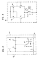
- a mask such as a photographic plate, is therefore associated with a neuron matrix of this type, the mask having zones whose transparencies differ in dependence on the weighting coefficients to be assigned to the various locations in the matrix.
- the matrix is then illuminated through the mask by a uniform-light source and the matrix thus becomes "specialised" to carry out the desired function.
- the mask by means of which the electrical resistances of the photosensitive elements of the matrix are defined has to be replaced in order to modify the function carried out by the net. Obviously, this kind of operation cannot be carried out continuously during processing.
- the neural net according to U.S. Patent No. 4,760,437 does not have a so-called “learning capability", that is, a capacity for the "on-line” alteration or up-dating of the weightings associated with at least some locations in the matrix.
- this object is achieved, by means of a neural data-processing net including active electronic devices associated with a matrix comprising a plurality of line electrodes, a plurality of column electrodes, and a plurality of ordered regions in which line electrodes and column electrodes are interconnected, the neural net being characterised in that at least some of the connecting regions of the matrix include electrochromic material.
Landscapes
- Engineering & Computer Science (AREA)
- Physics & Mathematics (AREA)
- Theoretical Computer Science (AREA)
- Health & Medical Sciences (AREA)
- Life Sciences & Earth Sciences (AREA)
- Biomedical Technology (AREA)
- Biophysics (AREA)
- Neurology (AREA)
- Mathematical Physics (AREA)
- Data Mining & Analysis (AREA)
- Evolutionary Computation (AREA)
- General Health & Medical Sciences (AREA)
- Molecular Biology (AREA)
- Computing Systems (AREA)
- General Engineering & Computer Science (AREA)
- General Physics & Mathematics (AREA)
- Computational Linguistics (AREA)
- Software Systems (AREA)
- Artificial Intelligence (AREA)
- Electrochromic Elements, Electrophoresis, Or Variable Reflection Or Absorption Elements (AREA)
- Image Processing (AREA)
- Pharmaceuticals Containing Other Organic And Inorganic Compounds (AREA)
- Electrotherapy Devices (AREA)
- Elevator Control (AREA)
- Exposure Control For Cameras (AREA)
- Peptides Or Proteins (AREA)
Applications Claiming Priority (2)
| Application Number | Priority Date | Filing Date | Title |
|---|---|---|---|
| IT6800689 | 1989-11-15 | ||
| IT06800689A IT1237269B (it) | 1989-11-15 | 1989-11-15 | Rete neurale con capacita' di apprendimento per il trattamento di informazioni, e procedimento per il trattamento di informazioni con l'impiego di tale rete. |
Publications (3)
| Publication Number | Publication Date |
|---|---|
| EP0433644A2 true EP0433644A2 (de) | 1991-06-26 |
| EP0433644A3 EP0433644A3 (en) | 1992-02-26 |
| EP0433644B1 EP0433644B1 (de) | 1995-10-04 |
Family
ID=11307139
Family Applications (1)
| Application Number | Title | Priority Date | Filing Date |
|---|---|---|---|
| EP90121486A Expired - Lifetime EP0433644B1 (de) | 1989-11-15 | 1990-11-09 | Neuronales Netz für Datenverarbeitung |
Country Status (5)
| Country | Link |
|---|---|
| US (1) | US5204937A (de) |
| EP (1) | EP0433644B1 (de) |
| AT (1) | ATE128779T1 (de) |
| DE (1) | DE69022828T2 (de) |
| IT (1) | IT1237269B (de) |
Cited By (1)
| Publication number | Priority date | Publication date | Assignee | Title |
|---|---|---|---|---|
| GB2316970A (en) * | 1996-09-05 | 1998-03-11 | Kenneth Scaddan | Threshold water excluding device which rises as a door closes |
Families Citing this family (7)
| Publication number | Priority date | Publication date | Assignee | Title |
|---|---|---|---|---|
| US6507828B1 (en) * | 1998-06-19 | 2003-01-14 | Jason Leonard | Neuron circuit and related techniques |
| US6763340B1 (en) * | 2000-09-22 | 2004-07-13 | The United States Of America As Represented By The Secretary Of The Air Force | Microelectromechanical system artificial neural network device |
| JP4256163B2 (ja) * | 2001-03-07 | 2009-04-22 | アクレオ アーベー | 電気化学ピクセル装置 |
| EP1487935A1 (de) * | 2002-03-07 | 2004-12-22 | Acreo AB | Elektrochemische vorrichtung |
| US7829162B2 (en) * | 2006-08-29 | 2010-11-09 | international imagining materials, inc | Thermal transfer ribbon |
| US10139693B2 (en) | 2015-06-19 | 2018-11-27 | International Business Machines Corporation | Synaptic electronic devices with electrochromic device |
| CN113504683A (zh) * | 2021-07-23 | 2021-10-15 | 中国科学技术大学 | 电致变色器件的制备方法与模仿人脑神经元传输信息的方法 |
Family Cites Families (16)
| Publication number | Priority date | Publication date | Assignee | Title |
|---|---|---|---|---|
| SU529467A1 (ru) * | 1975-07-21 | 1976-09-25 | Физико-Технический Институт Им. С.В.Стародубцева Ан Узбекской Сср | Электронно-оптический коррел тор |
| JPS5335565A (en) * | 1976-09-14 | 1978-04-03 | Sharp Corp | Electrochromic display device |
| US4335938A (en) * | 1979-08-30 | 1982-06-22 | American Cyanamid Company | Electrochromic cells with improved electrolyte system |
| US4392209A (en) * | 1981-03-31 | 1983-07-05 | Ibm Corporation | Randomly accessible memory display |
| NL8103377A (nl) * | 1981-07-16 | 1983-02-16 | Philips Nv | Weergeefinrichting. |
| US4498156A (en) * | 1981-09-24 | 1985-02-05 | Rockwell International Corporation | Electrochromic nonvolatile memory device |
| US4488781A (en) * | 1982-01-25 | 1984-12-18 | American Cyanamid Company | Method for manufacturing an electrochromic display device and device produced thereby |
| JPS59216177A (ja) * | 1983-05-25 | 1984-12-06 | 株式会社日立製作所 | 情報保持装置 |
| EP0192723A1 (de) * | 1984-09-07 | 1986-09-03 | PA Consulting Services Limited | Verfahren und anordnung zum übertragen von daten in einer integrierten halbleiterschaltungsanordnung |
| US4760437A (en) * | 1986-01-03 | 1988-07-26 | American Telephone And Telegraph Company, At&T Bell Laboratories | Neural networks |
| WO1989001228A1 (en) * | 1987-07-28 | 1989-02-09 | Maxdem Incorporated | Electrically settable resistance device |
| US4931763A (en) * | 1988-02-16 | 1990-06-05 | California Institute Of Technology | Memory switches based on metal oxide thin films |
| US4943556A (en) * | 1988-09-30 | 1990-07-24 | The United States Of America As Represented By The Secretary Of The Navy | Superconducting neural network computer and sensor array |
| US4916470A (en) * | 1988-11-16 | 1990-04-10 | Xerox Corporation | Image bar with electrochromic switching system |
| US5010512A (en) * | 1989-01-12 | 1991-04-23 | International Business Machines Corp. | Neural network having an associative memory that learns by example |
| US4969021A (en) * | 1989-06-12 | 1990-11-06 | California Institute Of Technology | Porous floating gate vertical mosfet device with programmable analog memory |
-
1989
- 1989-11-15 IT IT06800689A patent/IT1237269B/it active IP Right Grant
-
1990
- 1990-11-09 US US07/612,233 patent/US5204937A/en not_active Expired - Fee Related
- 1990-11-09 AT AT90121486T patent/ATE128779T1/de active
- 1990-11-09 DE DE69022828T patent/DE69022828T2/de not_active Expired - Fee Related
- 1990-11-09 EP EP90121486A patent/EP0433644B1/de not_active Expired - Lifetime
Cited By (1)
| Publication number | Priority date | Publication date | Assignee | Title |
|---|---|---|---|---|
| GB2316970A (en) * | 1996-09-05 | 1998-03-11 | Kenneth Scaddan | Threshold water excluding device which rises as a door closes |
Also Published As
| Publication number | Publication date |
|---|---|
| DE69022828T2 (de) | 1996-03-14 |
| EP0433644A3 (en) | 1992-02-26 |
| IT1237269B (it) | 1993-05-27 |
| ATE128779T1 (de) | 1995-10-15 |
| IT8968006A1 (it) | 1991-05-15 |
| DE69022828D1 (de) | 1995-11-09 |
| EP0433644B1 (de) | 1995-10-04 |
| US5204937A (en) | 1993-04-20 |
| IT8968006A0 (it) | 1989-11-15 |
Similar Documents
| Publication | Publication Date | Title |
|---|---|---|
| EP0377908B1 (de) | Neurales Netzwerk mit Assoziativspeicher, der durch Beispiele lernt | |
| Khalid | Review on various memristor models, characteristics, potential applications, and future works | |
| DE112018005726B4 (de) | Resistive verarbeitungseinheit auf zählerbasis für programmierbare und rekonfigurierbare künstliche neuronale netzwerke | |
| US4945257A (en) | Electrically settable resistance device | |
| EP0433644B1 (de) | Neuronales Netz für Datenverarbeitung | |
| Payvand et al. | On-chip error-triggered learning of multi-layer memristive spiking neural networks | |
| Merrikh-Bayat et al. | Memristor crossbar-based hardware implementation of the IDS method | |
| Hjelmfelt et al. | Implementation of logic functions and computations by chemical kinetics | |
| US20210034953A1 (en) | Reconfigurable finfet-based artificial neuron and synapse devices | |
| Kimura et al. | In–Ga–Zn–O thin-film devices as synapse elements in a neural network | |
| EP0411761B1 (de) | Neuronales Verarbeitungselement | |
| US6548316B1 (en) | Monolithic semiconductor device and method of manufacturing the same | |
| JP2009026181A (ja) | ニューラルネットワーク | |
| CN119296068B (zh) | 基于光电突触器件和忆阻器件的感存算一体化视觉系统 | |
| KR0183406B1 (ko) | 신경망에 사용되는 가중합가법의 용량성 구조물 | |
| Perez et al. | Neuromorphic-based Boolean and reversible logic circuits from organic electrochemical transistors | |
| US5220202A (en) | Memory device and memory apparatus using the same suitable for neural network | |
| CN112819148B (zh) | 基于浮栅晶体管的脉冲神经元网络 | |
| US5212377A (en) | Thin-film neuron network with optical programming | |
| US5440150A (en) | Non-crystalline silicon active device for large-scale digital and analog networks | |
| JP2926737B2 (ja) | 光情報処理装置 | |
| CN118613144A (zh) | 神经形态晶体管及制造方法、神经形态器件 | |
| KR102503360B1 (ko) | 시냅스 소자 및 이를 이용한 뉴로모픽 회로 | |
| CN117332824A (zh) | 基于加权和同步抖动算法的忆阻神经网络全电路 | |
| GB2255427A (en) | Neural networks |
Legal Events
| Date | Code | Title | Description |
|---|---|---|---|
| PUAI | Public reference made under article 153(3) epc to a published international application that has entered the european phase |
Free format text: ORIGINAL CODE: 0009012 |
|
| AK | Designated contracting states |
Kind code of ref document: A2 Designated state(s): AT BE CH DE DK ES FR GB GR LI LU NL SE |
|
| PUAL | Search report despatched |
Free format text: ORIGINAL CODE: 0009013 |
|
| AK | Designated contracting states |
Kind code of ref document: A3 Designated state(s): AT BE CH DE DK ES FR GB GR LI LU NL SE |
|
| 17P | Request for examination filed |
Effective date: 19920314 |
|
| 17Q | First examination report despatched |
Effective date: 19940503 |
|
| GRAA | (expected) grant |
Free format text: ORIGINAL CODE: 0009210 |
|
| AK | Designated contracting states |
Kind code of ref document: B1 Designated state(s): AT BE CH DE DK ES FR GB GR LI LU NL SE |
|
| PG25 | Lapsed in a contracting state [announced via postgrant information from national office to epo] |
Ref country code: GR Free format text: LAPSE BECAUSE OF FAILURE TO SUBMIT A TRANSLATION OF THE DESCRIPTION OR TO PAY THE FEE WITHIN THE PRESCRIBED TIME-LIMIT Effective date: 19951004 Ref country code: ES Free format text: THE PATENT HAS BEEN ANNULLED BY A DECISION OF A NATIONAL AUTHORITY Effective date: 19951004 Ref country code: DK Effective date: 19951004 Ref country code: AT Effective date: 19951004 |
|
| REF | Corresponds to: |
Ref document number: 128779 Country of ref document: AT Date of ref document: 19951015 Kind code of ref document: T |
|
| ET | Fr: translation filed | ||
| REF | Corresponds to: |
Ref document number: 69022828 Country of ref document: DE Date of ref document: 19951109 |
|
| PG25 | Lapsed in a contracting state [announced via postgrant information from national office to epo] |
Ref country code: LU Free format text: LAPSE BECAUSE OF NON-PAYMENT OF DUE FEES Effective date: 19951130 |
|
| PGFP | Annual fee paid to national office [announced via postgrant information from national office to epo] |
Ref country code: CH Payment date: 19951130 Year of fee payment: 6 |
|
| PG25 | Lapsed in a contracting state [announced via postgrant information from national office to epo] |
Ref country code: SE Effective date: 19960104 |
|
| REG | Reference to a national code |
Ref country code: CH Ref legal event code: PL |
|
| PLBE | No opposition filed within time limit |
Free format text: ORIGINAL CODE: 0009261 |
|
| STAA | Information on the status of an ep patent application or granted ep patent |
Free format text: STATUS: NO OPPOSITION FILED WITHIN TIME LIMIT |
|
| 26N | No opposition filed | ||
| PG25 | Lapsed in a contracting state [announced via postgrant information from national office to epo] |
Ref country code: LI Free format text: LAPSE BECAUSE OF FAILURE TO SUBMIT A TRANSLATION OF THE DESCRIPTION OR TO PAY THE FEE WITHIN THE PRESCRIBED TIME-LIMIT Effective date: 19961130 Ref country code: CH Free format text: LAPSE BECAUSE OF FAILURE TO SUBMIT A TRANSLATION OF THE DESCRIPTION OR TO PAY THE FEE WITHIN THE PRESCRIBED TIME-LIMIT Effective date: 19961130 |
|
| PGFP | Annual fee paid to national office [announced via postgrant information from national office to epo] |
Ref country code: DE Payment date: 20001030 Year of fee payment: 11 |
|
| PGFP | Annual fee paid to national office [announced via postgrant information from national office to epo] |
Ref country code: GB Payment date: 20001108 Year of fee payment: 11 |
|
| PGFP | Annual fee paid to national office [announced via postgrant information from national office to epo] |
Ref country code: FR Payment date: 20001110 Year of fee payment: 11 |
|
| PGFP | Annual fee paid to national office [announced via postgrant information from national office to epo] |
Ref country code: NL Payment date: 20001130 Year of fee payment: 11 |
|
| PGFP | Annual fee paid to national office [announced via postgrant information from national office to epo] |
Ref country code: BE Payment date: 20010123 Year of fee payment: 11 |
|
| PG25 | Lapsed in a contracting state [announced via postgrant information from national office to epo] |
Ref country code: GB Free format text: LAPSE BECAUSE OF NON-PAYMENT OF DUE FEES Effective date: 20011109 |
|
| PG25 | Lapsed in a contracting state [announced via postgrant information from national office to epo] |
Ref country code: BE Free format text: LAPSE BECAUSE OF NON-PAYMENT OF DUE FEES Effective date: 20011130 |
|
| REG | Reference to a national code |
Ref country code: GB Ref legal event code: IF02 |
|
| BERE | Be: lapsed |
Owner name: ENIRICERCHE S.P.A. Effective date: 20011130 |
|
| PG25 | Lapsed in a contracting state [announced via postgrant information from national office to epo] |
Ref country code: NL Free format text: LAPSE BECAUSE OF NON-PAYMENT OF DUE FEES Effective date: 20020601 |
|
| GBPC | Gb: european patent ceased through non-payment of renewal fee |
Effective date: 20011109 |
|
| PG25 | Lapsed in a contracting state [announced via postgrant information from national office to epo] |
Ref country code: DE Free format text: LAPSE BECAUSE OF NON-PAYMENT OF DUE FEES Effective date: 20020702 |
|
| PG25 | Lapsed in a contracting state [announced via postgrant information from national office to epo] |
Ref country code: FR Free format text: LAPSE BECAUSE OF NON-PAYMENT OF DUE FEES Effective date: 20020730 |
|
| NLV4 | Nl: lapsed or anulled due to non-payment of the annual fee |
Effective date: 20020601 |
|
| REG | Reference to a national code |
Ref country code: FR Ref legal event code: ST |
|
| REG | Reference to a national code |
Ref country code: FR Ref legal event code: ST |