EP0433742B1 - Module photosensible - Google Patents
Module photosensible Download PDFInfo
- Publication number
- EP0433742B1 EP0433742B1 EP90123080A EP90123080A EP0433742B1 EP 0433742 B1 EP0433742 B1 EP 0433742B1 EP 90123080 A EP90123080 A EP 90123080A EP 90123080 A EP90123080 A EP 90123080A EP 0433742 B1 EP0433742 B1 EP 0433742B1
- Authority
- EP
- European Patent Office
- Prior art keywords
- photo
- carrier plate
- module
- integrated circuit
- connecting conductor
- Prior art date
- Legal status (The legal status is an assumption and is not a legal conclusion. Google has not performed a legal analysis and makes no representation as to the accuracy of the status listed.)
- Expired - Lifetime
Links
Images

Classifications
-
- H—ELECTRICITY
- H10—SEMICONDUCTOR DEVICES; ELECTRIC SOLID-STATE DEVICES NOT OTHERWISE PROVIDED FOR
- H10W—GENERIC PACKAGES, INTERCONNECTIONS, CONNECTORS OR OTHER CONSTRUCTIONAL DETAILS OF DEVICES COVERED BY CLASS H10
- H10W90/00—Package configurations
-
- H—ELECTRICITY
- H05—ELECTRIC TECHNIQUES NOT OTHERWISE PROVIDED FOR
- H05K—PRINTED CIRCUITS; CASINGS OR CONSTRUCTIONAL DETAILS OF ELECTRIC APPARATUS; MANUFACTURE OF ASSEMBLAGES OF ELECTRICAL COMPONENTS
- H05K1/00—Printed circuits
- H05K1/02—Details
- H05K1/0274—Optical details, e.g. printed circuits comprising integral optical means
-
- H—ELECTRICITY
- H05—ELECTRIC TECHNIQUES NOT OTHERWISE PROVIDED FOR
- H05K—PRINTED CIRCUITS; CASINGS OR CONSTRUCTIONAL DETAILS OF ELECTRIC APPARATUS; MANUFACTURE OF ASSEMBLAGES OF ELECTRICAL COMPONENTS
- H05K1/00—Printed circuits
- H05K1/18—Printed circuits structurally associated with non-printed electric components
- H05K1/181—Printed circuits structurally associated with non-printed electric components associated with surface mounted components
-
- H—ELECTRICITY
- H05—ELECTRIC TECHNIQUES NOT OTHERWISE PROVIDED FOR
- H05K—PRINTED CIRCUITS; CASINGS OR CONSTRUCTIONAL DETAILS OF ELECTRIC APPARATUS; MANUFACTURE OF ASSEMBLAGES OF ELECTRICAL COMPONENTS
- H05K3/00—Apparatus or processes for manufacturing printed circuits
- H05K3/22—Secondary treatment of printed circuits
- H05K3/28—Applying non-metallic protective coatings
- H05K3/284—Applying non-metallic protective coatings for encapsulating mounted components
-
- H—ELECTRICITY
- H10—SEMICONDUCTOR DEVICES; ELECTRIC SOLID-STATE DEVICES NOT OTHERWISE PROVIDED FOR
- H10W—GENERIC PACKAGES, INTERCONNECTIONS, CONNECTORS OR OTHER CONSTRUCTIONAL DETAILS OF DEVICES COVERED BY CLASS H10
- H10W72/00—Interconnections or connectors in packages
- H10W72/50—Bond wires
- H10W72/541—Dispositions of bond wires
- H10W72/5449—Dispositions of bond wires not being orthogonal to a side surface of the chip, e.g. fan-out arrangements
Definitions
- the invention relates to a photo module according to the preamble of claim 1.
- Such a photo module is known from JP-A-58 204 573.
- a hybrid carrier plate built into a plastic housing has a photo diode and a light-emitting diode on one surface side and passive SMD (surface mounted devices) components and an integrated circuit (IC) in chip form on the other surface side. Neither the active nor the passive components are covered by a protective layer.
- JP-A-62 160 773 describes a photo module in which a photo diode and an IC are covered together on a carrier plate by a resin layer.
- a photo transistor and an IC are embedded together in a transparent resin layer.
- a black resin layer is applied to this transparent resin layer as light protection.
- this black resin layer does not offer sufficient light protection, since stray light can reach the IC through the transparent resin layer and cause interference there.
- the invention has for its object to provide an improved photo module in a small design, in which the most trouble-free possible signal processing is possible.
- the object is achieved by the features in the characterizing part of patent claim 1.
- Advantageous refinements and developments result from the subclaims.
- the photo module according to the invention has a hybrid carrier plate, on one surface side of which at least the photo-receiving element and an integrated circuit covered in chip form covered by black epoxy resin are arranged, while on the opposite surface side of the carrier plate further electrical components are arranged and interconnected.
- the two components can be brought very close to one another, so that the connection between them can also be made very short (for example 1.5 - 2.5 mm distance between the photodiode and the IC input).
- this can largely avoid unwanted repercussions in the circuit or interference from outside; on the other hand, a considerable reduction in the required area on the carrier plate can be achieved, which also results in cost savings due to the lower material requirement.
- connection between the components is carried out using a contacting method common in semiconductor technology; Thin aluminum-silicon wires are preferably used for this purpose with the aid of ultrasound technology.
- the wiring on the carrier plate is designed in such a way that all critical paths, which can cause positive feedback or feedback in the circuit, are shielded by appropriate ground conductors; these critical paths are the connection between the photodiode output and the input of the IC, the bond pads emanating from the components and the connecting interconnects to the external connecting pins, which are shielded or decoupled by ground lines or ground surfaces.
- peripheral circuitry of the photo module On the other surface side of the circuit board, further active and / or passive SMD components are arranged as peripheral circuitry of the photo module, which for example for filter adaptation, i. H. serve to select a specific frequency range.
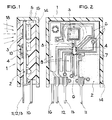
- the predetermined circuit arrangement with connecting conductor tracks 6, contact pads, through-contacts etc. is applied to a printed circuit board 2, preferably glass fiber epoxy laminate, by means of a photolithographic process. So that the active semiconductor chips 3, 4 can be contacted directly, a 1 to 2 »m thick nickel layer is galvanically grown on the copper interconnects and provided with a wafer-thin gold layer (thickness 0.05 - 0.3» m) for surface protection. Then, as is customary in SMD technology, solder paste (tin or lead) is applied to the back of the carrier plate using screen printing technology, and the passive components 5 of the circuit - resistors and capacitors - are applied with the aid of an automatic assembly machine and soldered in a reflow oven.
- solder paste titanium or lead
- the active components (photodiode 3 and IC 4) are now bonded as chip components using a silver epoxy adhesive to the front of the carrier plate and contacted by aluminum wires 7 (diameter, for example 25 »m) with about 1% silicon doping, the Making the contacts at room temperature with ultrasound support.
- the IC chip 4 is covered for protection against extraneous light and for mechanical stabilization with an opaque, black epoxy drop 10 (FIG. 1).
- the photodiode connection is protected with a translucent medium (preferably silicone).
- the connection electrodes 11, 12, 13 are connected to connection areas on the printed circuit board 2 by pressing, clamping or soldering.
- connection electrodes are necessary, which also reduces the peripheral wiring required.
- These connecting electrodes are preferably the power supply 11, the ground connection of the circuit 12 and the signal output 13 and run either parallel or perpendicular to the carrier plate 2.
- the circuit board is then introduced into a housing 14 consisting of a plastic body and potted using the potting compound 15.
- the housing 14 is contacted with a separate connection pin 16.
- the integrated circuit 4 contains a preamplifier, a logic circuit and a voltage stabilization circuit as essential circuit components.
- the passive components 5 are used to filter out a specific frequency range.
- the photo module is, for example, capable of IR remote control light pulses 18 with a frequency greater than 20 kHz to evaluate. However, the frequency range is determined by both the active and the passive components and can be expanded considerably by changing the necessary components.
- the bandwidth of the photo module is, for example, 3 to 6 kHz.
Landscapes
- Engineering & Computer Science (AREA)
- Microelectronics & Electronic Packaging (AREA)
- Light Receiving Elements (AREA)
Claims (8)
- Module photosensible (1) comprenant, sur une face d'une plaque support hybride (2), au moins l'élément photorécepteur, constitué par une photodiode (3), ainsi qu'un circuit intégré (4), sous la forme de puces, de même que, sur la face opposée de la plaque support (2), des composants (5) actifs et passifs du type des composants pour montage en surface (CMS) qui sont interconnectés, caractérisé en ce que la plaque support (2) est en résine époxy-fibre de verre, sur laquelle sont appliquées des pistes conductives de raccordement (6), que la piste conductive de liaison (8) entre la photodiode (3) et le circuit intégré (4), les contacts des composants ainsi que les pistes conductives de raccordement (6), sont blindés par des conducteurs de masse (9) ou des surfaces mises à la masse, que le circuit intégré (4) est recouvert d'une résine époxy noire opaque (10) et que la plaque support (2) est entièremement encapsulée dans une pièce (14) en matière plastique.
- Module photosensible selon la revendication 1, caractérisé en ce que la photodiode (3) et le circuit intégré (4) sont placés directement l'un à côté de l'autre.
- Module photosensible selon une des revendications précédentes, caractérisé en ce que la plaque support (2) possède seulement trois électrodes de raccordement externes (11, 12, 13).
- Module photosensible selon la revendication 3, caractérisé en ce que les trois électrodes de raccordement externes (11, 12, 13) de la plaque support (2) sont l'alimentation (11), la connexion à la masse (12) et la sortie de signal (13).
- Module photosensible selon la revendication 3 ou 4, caractérisé en ce que les électrodes de raccordement externes (11, 12, 13) sont reliées à des surfaces de raccordement sur la plaque support (2) et que les électrodes de raccordement (11, 12, 13) s'étendent ou bien parallèlement ou alors perpendiculairement à la plaque support (2).
- Procédé pour fabriquer un module photosensible selon une des revendications précédentes, caractérisé en ce que la photodiode (3) et le circuit intégré (4), sous la forme de puces, sont collés sur une face de la plaque support (2) au moyen d'une colle époxy à l'argent.
- Procédé selon la revendication 6, caractérisé en ce que le contact avec les composants actifs (3, 4) est établi au moyen de fils Al-Si (7) et avec le soutien d'ultrasons.
- Procédé selon la revendication 6 ou 7, caractérisé en ce que des pistes conductives de raccordement (6) en cuivre sont appliquées sur la plaque support (2), pistes qui sont ensuite nickelées et recouvertes d'une mince couche d'or.
Applications Claiming Priority (2)
| Application Number | Priority Date | Filing Date | Title |
|---|---|---|---|
| DE3941679A DE3941679A1 (de) | 1989-12-18 | 1989-12-18 | Fotomodul |
| DE3941679 | 1989-12-18 |
Publications (3)
| Publication Number | Publication Date |
|---|---|
| EP0433742A2 EP0433742A2 (fr) | 1991-06-26 |
| EP0433742A3 EP0433742A3 (en) | 1992-04-22 |
| EP0433742B1 true EP0433742B1 (fr) | 1995-08-02 |
Family
ID=6395655
Family Applications (1)
| Application Number | Title | Priority Date | Filing Date |
|---|---|---|---|
| EP90123080A Expired - Lifetime EP0433742B1 (fr) | 1989-12-18 | 1990-12-03 | Module photosensible |
Country Status (2)
| Country | Link |
|---|---|
| EP (1) | EP0433742B1 (fr) |
| DE (2) | DE3941679A1 (fr) |
Families Citing this family (3)
| Publication number | Priority date | Publication date | Assignee | Title |
|---|---|---|---|---|
| DE4440088A1 (de) * | 1994-11-10 | 1996-05-15 | Telefunken Microelectron | Halbleiterbaugruppe für die bidirektionale, leitungsungebundene, optische Datenübertragung |
| IT1302781B1 (it) * | 1998-10-08 | 2000-09-29 | Eliwell Spa Ora Invensys Clima | Circuiti integrati per strumenti elettronici di misura e/ocontrollo per la refrigerazione, il riscaldamento ed il |
| CN105504676B (zh) * | 2015-09-17 | 2017-10-10 | 天津盛远达科技有限公司 | 一种红外接收头封装用色素及其制备方法 |
Family Cites Families (15)
| Publication number | Priority date | Publication date | Assignee | Title |
|---|---|---|---|---|
| US3235945A (en) * | 1962-10-09 | 1966-02-22 | Philco Corp | Connection of semiconductor elements to thin film circuits using foil ribbon |
| US3934074A (en) * | 1974-04-22 | 1976-01-20 | Trw Inc. | Ceramic circuit board mounted in housing and method of fabrication thereof |
| CA1043911A (fr) * | 1975-04-14 | 1978-12-05 | Robert B. Johnson | Dispositif electronique sur substrat isolant |
| US4445274A (en) * | 1977-12-23 | 1984-05-01 | Ngk Insulators, Ltd. | Method of manufacturing a ceramic structural body |
| FR2439478A1 (fr) * | 1978-10-19 | 1980-05-16 | Cii Honeywell Bull | Boitier plat pour dispositifs a circuits integres |
| FR2503458A1 (fr) * | 1981-04-02 | 1982-10-08 | Cit Alcatel | Tete optique |
| US4514749A (en) * | 1983-01-18 | 1985-04-30 | At&T Bell Laboratories | VLSI Chip with ground shielding |
| DE3433779A1 (de) * | 1984-09-14 | 1986-03-27 | Robert Bosch Gmbh, 7000 Stuttgart | Schutzschicht fuer halbleiterschaltungen |
| DE3501806C2 (de) * | 1985-01-21 | 1986-11-13 | Philippe Zürich Vogt | Belichtungsmeßelement und damit ausgerüstete Belichtungsmeßvorrichtung |
| DD242308A1 (de) * | 1985-11-08 | 1987-01-21 | Werk Fernsehelektronik Veb | Multichiphybridbaustein |
| DE3619226A1 (de) * | 1985-12-10 | 1987-06-11 | Robotron Veb K | Verdrahtungstraeger |
| US4807036A (en) * | 1986-07-18 | 1989-02-21 | Tdk Corporation | Complex circuit component for a video signal circuit in a television receiver set |
| DE3779579D1 (de) * | 1986-12-02 | 1992-07-09 | Piller Gmbh Co Kg Anton | Modul mit halbleiter-leistungsschaltelementen. |
| US4758767A (en) * | 1987-05-15 | 1988-07-19 | Multipoint Control Systems, Incorporated | Self-contained analog photodiode light sensing head |
| DE8911283U1 (de) * | 1989-09-19 | 1989-11-02 | Fritz Kuke Kg, 1000 Berlin | Leiterplatte |
-
1989
- 1989-12-18 DE DE3941679A patent/DE3941679A1/de not_active Withdrawn
-
1990
- 1990-12-03 DE DE59009472T patent/DE59009472D1/de not_active Expired - Lifetime
- 1990-12-03 EP EP90123080A patent/EP0433742B1/fr not_active Expired - Lifetime
Non-Patent Citations (1)
| Title |
|---|
| PATENT ABSTRACTS OF JAPAN , vol. 8, no. 49 (E-230)6. März 1984 & JP-A-58 204 573 (SUMITOMO DENKI KOGYO K.K.) 29. November 1983 * |
Also Published As
| Publication number | Publication date |
|---|---|
| EP0433742A3 (en) | 1992-04-22 |
| DE59009472D1 (de) | 1995-09-07 |
| EP0433742A2 (fr) | 1991-06-26 |
| DE3941679A1 (de) | 1991-06-27 |
Similar Documents
| Publication | Publication Date | Title |
|---|---|---|
| DE10246892B4 (de) | LED-Matrix mit hoher Strahlungsleistung | |
| DE69129547T2 (de) | Packung für eine optoelektronische vorrichtung und verfahren zu ihrer herstellung | |
| DE69604333T2 (de) | Optisches Wellenleitermodul und Verfahren zu seiner Herstellung | |
| EP0083627B1 (fr) | Composant opto-electronique | |
| EP0111263B1 (fr) | Appareil de transmission ou réception contenant une diode dans une monture | |
| DE3633181A1 (de) | Verfahren zur herstellung eines optokopplers bzw. einer reflexlichtschranke und zugehoeriger optokoppler bzw. zugehoerige reflexlichtschranke | |
| DE3633251A1 (de) | Optoelektronisches koppelelement | |
| DE102009018644B4 (de) | Induktives Sensormodul und induktiver Näherungssensor | |
| EP0712161B1 (fr) | Elément semi-conducteur pour une transmission optique de données bidirectionnelle en espace libre | |
| DE19643911A1 (de) | Schaltungsanordnung mit auf einem mit Leiterbahnen versehenen Substrat angebrachten optoelektronischen Bauelementen | |
| DE2601956C3 (de) | Optoelektronisches Koppelelement | |
| DE2734798C2 (fr) | ||
| DE10227544B4 (de) | Vorrichtung zur optischen Datenübertragung | |
| DE102005047170A1 (de) | Optische Vorrichtung, optischer Verbinder und damit ausgerüstete elektronische Einrichtung | |
| EP0868778B1 (fr) | Composant electronique, notamment composant fonctionnant a l'aide d'ondes de surface acoustiques (composant a ondes de surface) | |
| DE102005046164A1 (de) | Röntgendetektor | |
| DE19702186C2 (de) | Verfahren zur Gehäusung von integrierten Schaltkreisen | |
| EP0433742A2 (fr) | Module photosensible | |
| DE19622650A1 (de) | Gehäuse für digitalen Hochleistungs-IC, welcher ein BGA(Kugelgitterarray)-Ein/Ausgabe-Format verwendet sowie keramisches Einschicht-Substrat mit Bimetall gefüllter Durchgangstechnologie | |
| CH616277A5 (en) | Semiconductor diode device for generating or for receiving radiation. | |
| DE10310616B3 (de) | Modul mit Schaltungsträger und elektrooptischem Wandler sowie Verfahren zur Herstellung desselben | |
| WO2018024705A1 (fr) | Module à multiples puces | |
| WO1996024162A1 (fr) | Boitier de puce et son procede de production | |
| DE19917438A1 (de) | Schaltungsanordnung und Verfahren zu ihrer Herstellung | |
| DE69117620T2 (de) | Kompaktes Bilderzeugungsgerät mit verbesserten optischen Eigenschaften für elektronische Endoskope |
Legal Events
| Date | Code | Title | Description |
|---|---|---|---|
| PUAI | Public reference made under article 153(3) epc to a published international application that has entered the european phase |
Free format text: ORIGINAL CODE: 0009012 |
|
| AK | Designated contracting states |
Kind code of ref document: A2 Designated state(s): DE FR GB IT |
|
| PUAL | Search report despatched |
Free format text: ORIGINAL CODE: 0009013 |
|
| AK | Designated contracting states |
Kind code of ref document: A3 Designated state(s): DE FR GB IT |
|
| 17P | Request for examination filed |
Effective date: 19920616 |
|
| 17Q | First examination report despatched |
Effective date: 19920727 |
|
| RAP1 | Party data changed (applicant data changed or rights of an application transferred) |
Owner name: TEMIC TELEFUNKEN MICROELECTRONIC GMBH |
|
| GRAA | (expected) grant |
Free format text: ORIGINAL CODE: 0009210 |
|
| AK | Designated contracting states |
Kind code of ref document: B1 Designated state(s): DE FR GB IT |
|
| ITF | It: translation for a ep patent filed | ||
| GBT | Gb: translation of ep patent filed (gb section 77(6)(a)/1977) |
Effective date: 19950807 |
|
| REF | Corresponds to: |
Ref document number: 59009472 Country of ref document: DE Date of ref document: 19950907 |
|
| ET | Fr: translation filed | ||
| PLBE | No opposition filed within time limit |
Free format text: ORIGINAL CODE: 0009261 |
|
| STAA | Information on the status of an ep patent application or granted ep patent |
Free format text: STATUS: NO OPPOSITION FILED WITHIN TIME LIMIT |
|
| 26N | No opposition filed | ||
| REG | Reference to a national code |
Ref country code: GB Ref legal event code: 732E |
|
| REG | Reference to a national code |
Ref country code: FR Ref legal event code: TP |
|
| REG | Reference to a national code |
Ref country code: GB Ref legal event code: IF02 |
|
| PGFP | Annual fee paid to national office [announced via postgrant information from national office to epo] |
Ref country code: GB Payment date: 20091218 Year of fee payment: 20 Ref country code: IT Payment date: 20091223 Year of fee payment: 20 Ref country code: FR Payment date: 20100108 Year of fee payment: 20 |
|
| PGFP | Annual fee paid to national office [announced via postgrant information from national office to epo] |
Ref country code: DE Payment date: 20091222 Year of fee payment: 20 |
|
| REG | Reference to a national code |
Ref country code: GB Ref legal event code: PE20 Expiry date: 20101202 |
|
| PG25 | Lapsed in a contracting state [announced via postgrant information from national office to epo] |
Ref country code: GB Free format text: LAPSE BECAUSE OF EXPIRATION OF PROTECTION Effective date: 20101202 |
|
| PG25 | Lapsed in a contracting state [announced via postgrant information from national office to epo] |
Ref country code: DE Free format text: LAPSE BECAUSE OF EXPIRATION OF PROTECTION Effective date: 20101203 |