EP0434033A2 - Dispositif d'affichage à cristaux liquides - Google Patents
Dispositif d'affichage à cristaux liquides Download PDFInfo
- Publication number
- EP0434033A2 EP0434033A2 EP90124774A EP90124774A EP0434033A2 EP 0434033 A2 EP0434033 A2 EP 0434033A2 EP 90124774 A EP90124774 A EP 90124774A EP 90124774 A EP90124774 A EP 90124774A EP 0434033 A2 EP0434033 A2 EP 0434033A2
- Authority
- EP
- European Patent Office
- Prior art keywords
- voltage
- signal
- scanning
- correcting
- liquid crystal
- Prior art date
- Legal status (The legal status is an assumption and is not a legal conclusion. Google has not performed a legal analysis and makes no representation as to the accuracy of the status listed.)
- Granted
Links
Images


Classifications
-
- G—PHYSICS
- G09—EDUCATION; CRYPTOGRAPHY; DISPLAY; ADVERTISING; SEALS
- G09G—ARRANGEMENTS OR CIRCUITS FOR CONTROL OF INDICATING DEVICES USING STATIC MEANS TO PRESENT VARIABLE INFORMATION
- G09G3/00—Control arrangements or circuits, of interest only in connection with visual indicators other than cathode-ray tubes
- G09G3/20—Control arrangements or circuits, of interest only in connection with visual indicators other than cathode-ray tubes for presentation of an assembly of a number of characters, e.g. a page, by composing the assembly by combination of individual elements arranged in a matrix no fixed position being assigned to or needed to be assigned to the individual characters or partial characters
- G09G3/34—Control arrangements or circuits, of interest only in connection with visual indicators other than cathode-ray tubes for presentation of an assembly of a number of characters, e.g. a page, by composing the assembly by combination of individual elements arranged in a matrix no fixed position being assigned to or needed to be assigned to the individual characters or partial characters by control of light from an independent source
- G09G3/36—Control arrangements or circuits, of interest only in connection with visual indicators other than cathode-ray tubes for presentation of an assembly of a number of characters, e.g. a page, by composing the assembly by combination of individual elements arranged in a matrix no fixed position being assigned to or needed to be assigned to the individual characters or partial characters by control of light from an independent source using liquid crystals
- G09G3/3611—Control of matrices with row and column drivers
- G09G3/3674—Details of drivers for scan electrodes
- G09G3/3681—Details of drivers for scan electrodes suitable for passive matrices only
-
- G—PHYSICS
- G09—EDUCATION; CRYPTOGRAPHY; DISPLAY; ADVERTISING; SEALS
- G09G—ARRANGEMENTS OR CIRCUITS FOR CONTROL OF INDICATING DEVICES USING STATIC MEANS TO PRESENT VARIABLE INFORMATION
- G09G3/00—Control arrangements or circuits, of interest only in connection with visual indicators other than cathode-ray tubes
-
- G—PHYSICS
- G09—EDUCATION; CRYPTOGRAPHY; DISPLAY; ADVERTISING; SEALS
- G09G—ARRANGEMENTS OR CIRCUITS FOR CONTROL OF INDICATING DEVICES USING STATIC MEANS TO PRESENT VARIABLE INFORMATION
- G09G2320/00—Control of display operating conditions
- G09G2320/02—Improving the quality of display appearance
- G09G2320/0209—Crosstalk reduction, i.e. to reduce direct or indirect influences of signals directed to a certain pixel of the displayed image on other pixels of said image, inclusive of influences affecting pixels in different frames or fields or sub-images which constitute a same image, e.g. left and right images of a stereoscopic display
-
- G—PHYSICS
- G09—EDUCATION; CRYPTOGRAPHY; DISPLAY; ADVERTISING; SEALS
- G09G—ARRANGEMENTS OR CIRCUITS FOR CONTROL OF INDICATING DEVICES USING STATIC MEANS TO PRESENT VARIABLE INFORMATION
- G09G2320/00—Control of display operating conditions
- G09G2320/04—Maintaining the quality of display appearance
- G09G2320/041—Temperature compensation
Definitions
- the present invention relates to a liquid crystal display device.
- a matrix type liquid crystal display device is provided with scanning electrodes and signal electrodes forming picture elements (pixels) at each crossing point between a scanning electrode and a signal electrode.
- the electrical resistance of the scanning electrodes and the signal electrodes is not zero and a capacitor is formed at those crossing points with the liquid crystal layer forming the dielectric. Therefore, the effective voltage applied via the scanning electrodes and the signal electrodes to the individual pixels changes in accordance with the content of the display, i.e. the displayed image.
- the unevenness of the display can be further improved by a voltage correcting method suggested in the Japanese patent application 63-159914, although even with this method the display is still not sufficiently uniform as will be explained below.
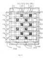
- Fig. 14 shows a liquid crystal panel 1 representing a specific display pattern which will be used for the following explanation.
- the liquid crystal panel comprises a pair of substrates 2, 3 sandwiching a liquid crystal layer (not shown).
- a plurality of scanning electrodes Y1 through Y6 is provided on the side of the substrate 2 facing the liquid crystal layer and a plurality of signal electrodes X1 through X6 is provided on the opposing side of the substrate 3, the signal electrodes extending perpendicularly with respect to the scanning electrodes.
- a pixel display dot
- the example shown in Fig. 14 comprises 6 x 6 pixels for the sake of simplification of the explanation only. In a practical liquid crystal panel the number of pixels is substantially higher.
- the hatched pixels are lighting pixels whereas the other pixels are non-lighting pixels.
- the display pattern shown in Fig. 14 is a chequered pattern.
- To the left side of the scanning electrodes Y1 through Y6 a corrected scanning voltage wave is applied to every other scanning electrode, said corrected scanning voltage wave varying dependent on the display pattern in accordance with the voltage correcting method disclosed in the Japanese patent application No. 63-159914.
- the non-selective voltage is superimposed with a correcting voltage in accordance with the difference between the number of lighting pixels on a scanning electrode and the number of lighting pixels on the following scanning electrode when the selection is moved from one scanning electrode to the following one.
- the said difference is always zero, no correcting voltage is superimposed on the non-selective voltage.
- the signal electrodes X1 through X6 are divided into two groups, a first group of signal electrodes X1, X3 and X5 having applied the signal voltage wave at the upper end of the liquid crystal display panel 1 in Fig. 14, and a second group of signal electrodes X2, X4 and X6 having applied the signal voltage wave at the lower end of the liquid crystal display panel in Fig. 14.
- the liquid crystal panel 1 is of the so-called "positive display" type where a pixel turns dark when the applied effective voltage exceeds a certain threshold value.
- the pixels on the signal electrodes X3 and X5 will be brighter (less dark) in the upper portion and darker in the lower portion of the display panel.
- the pixels formed on the signal electrodes X2, X4 and X6 will become brighter in the lower portion and darker in the upper portion of the display panel.
- the actually applied effective voltage becomes the lower the nearer a pixel is located to the driving end of a signal electrode, i.e. the side to which the signal voltage wave is applied.
- Figs. 15(a) through (c) show each a voltage wave used to drive the liquid crystal panel of Fig. 14.
- the full line shows the voltage wave at the signal electrode X3 in the position of the pixel D31 in Fig. 14.
- the dotted line shows the voltage wave at the signal electrode X2 in the position of the pixel D21.
- the full line and the dotted line are drawn side by side to make them distinguishable, although they would be actually overlapping.
- Fig. 15(b) shows the voltage wave at the signal electrode X1 in the position of the scanning electrode Y1, i.e. corresponding to the position of pixels D21 and D31.
- FIG. 15(c) shows the voltage difference between the voltage wave at the scanning electrode Y1 and the two voltage waves of Fig. 15(a), respectively, i.e. the full line in Fig. 15(c) corresponds to the voltage applied to the pixel D31 and the dotted line corresponds to the voltage applied to the pixel D21.
- the hatched portions in Fig. 15 show the difference between the voltages applied to the lighting pixel D31 and the non-lighting pixel D21, which is not the voltage difference causing the unevenness of display.
- Fig. 15 shows the voltage difference between the voltage wave at the scanning electrode Y1 and the two voltage waves of Fig. 15(a), respectively, i.e. the full line in Fig. 15(c) corresponds to the voltage applied to the pixel D31 and the dotted line corresponds to the voltage applied to the pixel D21.
- the hatched portions in Fig. 15 show the difference between the voltages applied to the lighting pixel D31 and the non-lighting pixel D21,
- V5, V3, V0 and V4 are lighting, non-lighting, selective and non-selective voltages of a first group of voltages
- V0, V2, V5 and V1 are the lighting, non-lighting, selective and non-selective voltages of a second group of voltages.
- the selective and non-selective voltages are applied to the scanning electrodes as scanning voltage wave
- the lighting and the non-lighting voltages are applied to the signal electrodes as the signal voltage wave.
- the first and second voltage groups are periodically switched. In this example, switching is performed each time when all the scanning electrodes Y1 through Y6 have been applied with the selective voltage (this cycle is called one frame, and two frames F1 and F2 are shown in the Fig.).
- a spike type noise is generated in the scanning electrode Y1 which is larger than that when the voltage at the signal electrodes X2, X4 and X6 is changed from the lighting (non-lighting) voltage to the non-lighting (lighting) voltage.
- the spike type noise generated in the scanning electrode Y1 by the said switching of the voltage at the signal electrodes X1, X3 and X5 dominates the spike type noise generated in the scanning electrode Y1 by the corresponding switching of the voltage at the signal electrodes X2, X4 and X6. Therefore, as shown by the full line voltage wave in Fig. 15(c), the effective voltage applied to the pixel D31 becomes lower than that applied to the pixel D21 which is represented by the dotted line.
- the corresponding noise generated in the scanning electrode Y6 of Fig. 14 is dominated by the voltage switching at the signal electrodes X2, X4 and X6. Therefore, the effective voltage applied to the pixel D26 becomes lower than that applied to the pixel D36.
- Yn designates the n-th scanning electrode from the upper side in Fig. 14.
- Xm designates the m-th signal electrode from left side in Fig. 14.
- Dmn designates the pixel formed at the crossing point of the signal electrode Xm and the scanning electrode Yn.
- the signal electrodes are divided into two groups, a first group having the driving end at the upper side in Fig. 14 and a second group having the driving end at the lower side.
- the pixels (Dmn, Dmn+1) formed between any of the signal electrodes (X1, X3, X5) of the first group and the scanning electrodes Yn and Yn+1 are both lighting, this is defined as a1, when both are non-lighting it is defined as b1.
- the pixel Dmn is lighting and the pixel Dmn+1 is non-lighting, it is defined as c1 and if the pixel Dmn is non-lighting and the pixel Dmn+1 is lighting, it is defined as d1.
- the pixels (Dmn, Dmn+1) formed between any of the signal electrodes (X2, X4, X6) of the second group and the scanning electrodes Yn and Yn+1 are both lighting, it is defined as a2 and when they are both non-lighting it is defined as b2.
- the pixel Dmn is lighting and the pixel Dmn+1 is non-lighting, it is defined as c2 while, when the pixel Dmn is non-lighting and the pixel Dmn+1 is lighting, it is defined as d2.
- N1 ON and N1 OFF are the number of those pixels formed by the scanning electrode Yn and all signal electrodes of the first group, which are lighting and non-lighting, respectively.
- M1 ON and M1 OFF are the corresponding numbers of lighting and non-lighting pixels formed between the scanning electrode Yn+1 and the signal electrodes of the first group.
- N2 ON , N2 OFF , M1 ON and M2 OFF are the corresponding numbers of pixels formed with the signal electrodes of the second group.
- a numeric value I1 is defined as
- a numeric value I2 is defined as
- I(k) f(k) * I1 + f(L-k) * I2.
- f(k) is a weighting function becoming smaller as k becomes larger.
- the weighting function f(k) it is considered that the spike type noise generated by a signal electrode in a scanning electrode is the larger the nearer the scanning electrode is to the driving end of the respective signal electrode.
- L indicates the total number of scanning electrodes and k is 1 ⁇ k ⁇ L.
- a spike type noise according to the absolute value of the function I(k) is generated in the k-th scanning electrode Yk when the selection is moved from the scanning electrode Yn to the scanning electrode Yn+1. Namely, when the value of the function I(k) becomes larger, the noise will be larger.
- the direction of this noise depends on whether the value of the function I(k) is positive or negative. If the direction of the voltage of the spike type noise according to the function I(k) and the variation of the voltage wave applied to a signal electrode are in phase, the effective voltage applied to the pixel formed between this signal electrode and this scanning electrode Yk becomes lower to brighten the display. If the phases are opposite, the effective voltage becomes higher to darken the display.
- Figs. 16 and 17 show the same liquid crystal panel with different display patterns.
- the liquid crystal panel 1 has the same structure as that of Fig. 14 and the same reference numerals are used.
- the scanning voltage wave is applied to the left side of the scanning electrodes Y1 through Y6 in Figs. 16 and 17.
- the scanning voltage wave varies dependent on the display pattern to improve an unevenness due to the "weft pulling" in accordance with a method described in the Japanese patent application 63-159914. That is, a correcting voltage is superimposed to the selective voltage in accordance with the number Z of lighting pixels on the scanning electrode to be selected.
- the display patterns in Fig. 16 and 17 are congruent quadrangles, positioned at the left end in Fig. 16 and at the right end in Fig. 17. Therefore, in order to achieve the display patterns of Figs. 16 and 17 according to the above method, completely the same correcting voltage will be applied to each scanning electrode Y1 through Y6.
- the function q(i) is a weighting function increasing as i increases.
- the function ⁇ (i) becomes 1 when the pixel formed by the selected scanning electrode and the signal electrode Xi is lighting, and it becomes 0 when this pixel is non-lighting. Therefore, the numerical value Z' represents the number of lighting pixels each weighted by its distance from the driving end of the scanning electrode.
- the invention as claimed is intended to remedy the above explained drawbacks of the prior art and to provide a liquid crystal display device having an improved evenness of the display and, thus, a better display quality, irrespective of the pattern or subject to be displayed.
- the liquid crystal display device comprises a liquid crystal panel having a pair of substrates sandwiching a liquid crystal layer therebetween, wherein one of the substrates is provided with a group of scanning electrodes and the other with a group of signal electrodes.
- the liquid crystal display device further comprises means for applying a scanning voltage wave to at least one end of the scanning electrodes and for applying a signal voltage wave to at least one end of the signal electrodes to display images, characters, etc.
- display pattern means for superimposing a correcting voltage to at least one of the scanning voltage wave and the signal voltage wave in accordance with the display pattern, and means for varying the value of the correcting voltage in accordance with pixels' or the scanning electrode's distance from the driving end of the scanning electrodes and/or from the driving end of the signal electrodes.
- the value of the correcting voltage is varied for each scanning electrode or each signal electrode.
- the invention allows to supply a correcting voltage considering the relation between a display position within a display pattern and the driving end of an electrode.
- a first embodiment of the present invention will be described with reference to Figs. 1 to 7. As an example it will be shown how the present invention avoids an unevenness of the display when a chequered pattern is displayed.
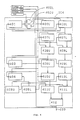
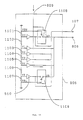
- Fig. 1 shows a block diagram of the first embodiment.
- 101 designates a liquid crystal unit details of which are shown in and will be explained with reference to Fig. 2.
- Numeral 102 designates a sequential control signal for controlling the operation of the liquid crystal display device, the sequential control signal including a latch signal LP, a frame signal FR, a data-in signal DIN, an X driver shift clock signal XSCL and others.
- Numeral 103 designates a data signal which determines the display pattern. Changes in the data signal 103 are synchronized with the leading edges of the signal XSCL.
- the data signal 103 is supplied to the liquid crystal unit 101 and to a voltage correcting circuit 104 at the trailing edges of the signal XSCL.
- Numeral 105 designates a power source circuit and numeral 108 a divider circuit for providing a clock signal 110 (referred to as correcting clock hereinafter) which is synchronized with the signal LP.
- Numeral 106 designates Y voltages, i.e. voltages for driving the scanning electrodes.
- Numeral 107 designates X voltages, i.e. voltages for driving the signal electrodes.
- Numeral 109 designates correcting signals output from the voltage correcting circuit 104.
- the liquid crystal unit 101 is shown to comprise a liquid crystal panel 201, an Y driver 205 which is a circuit for driving the scanning electrodes, and an X driver 213 which is a circuit for driving the signal electrodes.
- the liquid crystal panel 201 comprises a pair of substrates 202 and 203 sandwiching a liquid crystal layer therebetween. Scanning electrodes Y1 through Y6 are arranged on the substrate 202 and signal electrodes X1 through X6 on the substrate 203. The signal electrodes X1 through X6 extend perpendicularly to the scanning electrodes Y1 through Y6.
- the signal electrodes X1, X3 and X5 have respective terminals for applying the signal voltage wave on the upper side of the liquid crystal panel (in Fig. 2), while the signal electrodes X2, X4 and X6 have their respective terminals on the lower side.
- a pixel 204 is formed at each crossing point between the scanning electrodes Y1 through Y6 and the signal electrodes X1 through X6.
- the liquid crystal panel is described to have six scanning electrodes and six signal electrodes forming 6 x 6 pixels. This is a relatively small number used for the sake of simplification of the explanation. In a practical embodiment, the number of signal and scanning electrodes may be higher.
- the Y driver 205 comprises a shift register circuit 206, a shift register circuit 207, a latch circuit 208, a counter circuit 209, a coincidence detector circuit 210, a switch circuit 211 and a level shifter circuit 212.
- Each stage of the shift register circuit 207 has a plurality of bits which are shifted simultaneously, i.e. in parallel (in the present embodiment each stage has five bits).
- the shift register 206 is supplied with the signal DIN at the trailing edge of the signal LP and transfers the signal DIN sequentially into each of its stages at the following trailing edges of the signal LP.
- the signal DIN assumes a high electric potential "H” as the active "1” and is usually output once within an interval corresponding to the number of scanning electrodes Y1 through Y6 or the number of pulses of the signal LP which is equal to or higher than the number of scanning electrodes. Therefore, the data "1" is passed through the shift register 206 so that any time a control signal C0 output from one of the stages has the state "1" while those of the other stages have the state "0".
- each stage of the shift register 207 comprises five bits.
- This shift register is operated by a Y correcting shift clock (referred to a signal "YCSCL" hereinafter) to sequentially take in and shift the correcting signals 109.
- the correcting signals contain four bits IB0 through IB3 of an intensity signal and one sign bit F.
- the intensity signal determines the value of the correcting voltage and the sign bit determines the polarity of the correcting voltage.
- the outputs of the shift register circuit 207 are taken into the latch circuit 208 under the control of the signal LP.
- the counter circuit 209 is an up-counter, having a number of bits corresponding to the number of the intensity signal bits IB0 through IB3.
- the counter circuit 209 counts up the correcting clock 110 and is reset by the signal LP.
- the coincidence detector circuit 210 includes a number of coincidence detectors corresponding to the number of stages of the shift register 207 and the latch circuit 208. Each coincidence detector compares the value in the respective stage of the latch circuit 208 with the output of the counter circuit 209. Each coincidence detector outputs a control signal C2 which changes from "0" to "1" when coincidence is detected. When the sign bit F which is output as control signal C1 is "1" indicating a negative value, the coincidence detectors detect the coincidence between the two's complement of the respective shift register value and the value of the output of the counter circuit 209. The result of the detection is held until the following signal LP is received.
- the switching circuit 211 receives the Y voltages 106 which are voltages V0, V1U, V1, V1L, V2, V3, V4U, V4, V4L and V5. These voltages are divided into a first voltage group consisting of V0, V4U, V4 and V4L, and a second voltage group consisting of V5, V1L, V1 and V1U.
- the switching circuit 211 switches from one to the other of the two voltage groups under the control of the signal FR.
- the voltages V0, V4U, V4 and V4L are the selective voltage, the correcting voltage (U), the non-selective voltage and the correcting voltage (L) of the first voltage group.
- the voltages V5, V1L, V1 and V1U are the selective voltage, the correcting voltage (U), the non-selective voltage and the correcting voltage (L) of the second voltage group.
- the correcting voltages (U) and (L) are simply called the correcting voltage.
- the level shifter circuit 212 contains a number of switches corresponding to the number of scanning lines Y1 to Y6, each switch having four input terminals S1 to S4 to be selectively connected to one output terminal.
- each switch selects S1, namely the selective voltage.
- each switch selects S3, namely the non-selective voltage.
- each switch selects S2 when the control signal C1 is “0” and selects S4, when the control signal C1 is "1".
- the shift register circuit 207 has been described to be a five bit shift register for the intensity signal bits IB0 through IB3 and the sign bit F. It is possible, however, to increase or decrease the number of bits by varying the bit number of the intensity signal.
- the number of stages of the shift register circuits 206 and 207, the latch circuit 108, the coincidence detector circuit 210 and the switching circuit 211 is the same as the number of scanning electrodes Y1 through Y6 of the liquid crystal panel.
- the signal DIN is taken into the shift register 206 in synchronism with the signal LP and is then shifted to the respective next stage of the shift register circuit 206 with each following signal LP, that is in a cyclically changing manner the output (control signal C0) of one of the stages of the shift register circuit 206 is "1" while the outputs of the other stages are “0". That one of the switches of the switching circuit 212 receiving a "1" as control signal C0 outputs the selective voltage and is called the “selected switch”, while the switches outputting other voltages are called “non-selected switches”.
- the level shifter circuit 212 outputs the selective voltage to a selected one of the scanning electrodes Y1 through Y6 and other voltages to the non-selected scanning electrodes.
- the intensity signal IB0 through IB3 and the sign bit F are taken into the shift register circuit 207 under the control of the signal YCSCL.
- the correcting voltage (U) or (L) is output from each non-selected switch until the absolute value of the intensity signal IB0 through IB3 coincides with the count value of the counter 209 clocked by the correcting clock signal.
- the control signal C1 determines whether the correcting voltage (U) or the correcting voltage (L) is output. In other words, it is determined whether the sign bit F is "0" or "1".
- each non-selected switch outputs the non-selective voltage. Therefore, the non-selected switches output the correcting voltage for a time period which corresponds to the absolute value of the intensity signal.
- Fig. 2 again to explain the X driver 213. It contains a shift register circuit 214, a latch circuit 215, and a level shifter circuit 216, each having a number of stages corresponding to the number of signal electrodes X1 through X6. The outputs of the level shifter circuit 216 are supplied to the signal electrodes X1 through X6, respectively.
- the shift register circuit 214 receives the data signal 103 under the control of the signal XSCL as the clock. As mentioned before, the data signal 103 determines the display pattern, i.e. indicates lighting or non-lighting of the pixels (herein, lighting is referred to as active "1" and non-lighting as non-active "0"). When all the data corresponding to the signal electrodes X1 through X6, namely corresponding to one row of pixels, have been input into the shift register circuit 214, these data are taken into the latch circuit 215 under the control of the signal LP. The level shifter circuit 216 outputs predetermined voltages in accordance with the contents of the latch circuit 215 and the status of the frame signal FR.
- the X voltages 107 comprise voltages V0, V2, V3 and V5. Like the scanning voltages the X voltages are divided into a first voltage group of voltages V5 and V3 and a second voltage group of voltages V0 and V2. Depending on the status of the frame signal FR either the first or the second voltage group is selected corresponding to the selection of the first or second voltage group in the Y driver 205.
- the voltages V5 and V3 are the lighting voltage and the non-lighting voltage of the first voltage group and the voltages V0 and V2 are the lighting voltage and the non-lighting voltage of the second voltage group.
- the corresponding stage of the level shifter circuit 216 outputs the lighting voltage of either voltage group depending on the signal FR to the respective signal electrode. If the output of the latch circuit is "0" the non-lighting voltage will be applied to the corresponding signal electrode.
- the liquid crystal unit 101 it is synchronized with the signals DIN and LP and the scanning electrodes Y1 through Y6 are sequentially supplied with the selective voltage while the lighting or the non-lighting voltage, corresponding to the display pattern, is synchronously supplied to the signal electrodes X1 through X6 in order to achieve the display by means of the liquid crystal panel 201.
- the scanning electrodes Y1 through Y6 which are not supplied with the selective voltage are instead of the non-selective voltage supplied the correcting voltage, having a length and polarity corresponding to the intensity signal I0 through I3 and the sign bit F of the correcting signal 109.
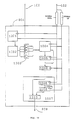
- a concrete example of the voltage correcting circuit 104 is given in Fig. 4 and will be explained in the following.
- numeral 401 designates a toggle flipflop circuit (referred to as T-F/F hereinafter)
- numerals 402U and 402L designate gate circuits
- numerals 403 and 404 counter circuits designate gate circuits
- numerals 405U and 405L function generator circuits designate gate circuits
- numerals 406U and 406L counter circuits designate gate circuits
- numerals 407U and 407L latch circuits numerals 408U and 408L arithmetic circuit for carrying out a subtraction
- numerals 409U and 409L memory elements numerals 410U and 410L latch circuits
- numerals 411U and 411L arithmetic circuits for carrying out a multiplication
- numeral 412 an arithmetic circuit for carrying out an addition and division.
- the T-F/F circuit is reset to "0" by the signal LP. Its output terminal is connected to a non-inverting input terminal of the gate 402U and to an inverting input terminal of the gate 402L.
- the status of the T-F/F circuit is reversed each time a clock signal XSCL is input. Therefore, when a data signal corresponding to any of the even number signal electrodes X2, X4 and X6 is entered into the gate circuits 402U and 402L in Fig. 4, it is passed only by the gate circuit 402L since the gate circuit 402U is blocked by the output of the T-F/F circuit.
- the T-F/F circuit and the gate circuits 402U and 402L thus serve to separate the data signals corresponding to the top driven signal electrodes from the data signals corresponding to the bottom driven signal electrodes.
- the top driven signal electrodes are those having their driving end in the upper portion of the liquid crystal panel 201 in Fig. 2, while the bottom driven signal electrodes have their driving end in the lower portion.
- the separated data signals are defined as "upper data signal” and "lower data signal".
- the counters 406U and 406L separately count the number of the condition "1", i.e. the lighting condition, in the separated data signals.
- the counters 406U and 406L carry out an addition only when the output of the gate 402U and the gate 402L, respectively, is "1".
- the count values of the counters 406U and 406L are defined as M1 ON and M2 ON . These values are taken into the latch circuit 407U and 407L in synchronism with the signal LP.
- the values in the latch circuits 407U and 407L are defined as N1 ON and N2 ON .
- the counter 403 is an up-counter circuit serving as an address generator for generating addresses for the memory elements 409U and 409L corresponding to the number of scanning electrodes Y1 through Y6. In the present example the counter counts from 0 to 5 and is reset to 0 by the signal DIN.
- the address output from the counter 403 is 0 when the differences I1 and I2 calculated by the arithmetic circuits 408U and 408L are those for the first and the second scanning line, i.e. Y1 and Y2 in the present example.
- the address output from the counter 403 is 1 when the differences I1 and I2 are those for the second and the third scanning lines Y2 and Y3, etc.
- the above mentioned numerical values I1 and I2 are thus written in the memory elements 409U and 409L under the addresses indicated by the counter 403.
- the counters 406U and 406L count the number of lighting pixels M1 ON and M2 ON on the scanning electrode Yn+1 while the selective voltage is applied to the scanning electrode Yn. At this time the number of lighting pixels N1 ON and N2 ON on the scanning electrode Yn is held in the latch circuits 408U and 408L. Shortly before the selective voltage is applied to the scanning electrode Yn+1, the differences I1 and I2 are calculated and written into the memory elements 409U and 409L under the address of n-1.
- This operation is repeated by cyclically changing the value of n through 1 to 6, that is, in the memory elements 409U and 409L the differences I1 and I2 of the number of lighting pixels on the scanning electrodes Y1 and Y2 are stored under the address of 0. Under the addresses of 1 through 5 the differences I1 and I2 between the numbers of lighting pixels on each pair of scanning electrodes Y2 and Y3, Y3 and Y4, Y4 and Y5, and Y5 and Y1 are stored.
- the counter 404 is an up-counter circuit which in the present example counts from 0 to 5 and is reset to 0 by the signal LP.
- the possible number of count values of the counter 404 corresponds to the number of scanning electrodes Y1 through Y6.
- the signal XSCL fulfils this condition and is used as the signal YCSCL.
- the output of the counter 404 is used as a variable for the function generator circuit 405U and 405L.
- the function generator circuits 405U and 405L contain a numerical value table provided in a read-only memory (referred to as "ROM" hereinafter) and a diode matrix. The output of these circuits is the value of a function of the input variable.
- the function generator circuit 405U contains the table for returning the value of the function f(k) (wherein k designates the variable which may also be considered as an address).
- the value of the function f(k) decreases as the variable k increases.
- f(k) is the weighting function used for considering the influence of the distance between a respective scanning electrode and the driving ends of the signal electrodes.
- the function values may be obtained, for example, from an experiment.
- the function generator circuit 405L returns upon input of a variable k the value of the function f(L-k).
- the arithmetic circuits 411U and 411L in Fig. 4 multiply the values stored in the memory elements 409U and 409L under the address (n-1) indicated by the counter 403 with the values returned by the function generator circuits 405U and 405L, respectively. Since the counter 404 is up-counted by the signal YCSCL, the value output from the function generator circuits 405U and 405L is varied in synchronism with the signal YCSCL. In other words, the result of the operation of the arithmetic circuits 411U and 411L becomes as listed below and is synchronized with the signal YCSCL.
- the result comprising the intensity signal with bits IB0 through IB3 and the sign bit F is then output as the correcting signal 109 synchronized with the signal YCSCL.
- the structure of the voltage correcting circuit 104 is not limited to the above explained one. For example, instead of calculating the result I on a real-time basis, it would be possible to calculate it previously by a CPU, write it into a memory provided for this purpose and read out the correcting signal 109 under the control of the address counter 404.
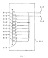
- FIG. 5 An example of a concrete structure of the power source circuit 101 of Fig. 1 is shown in Fig. 5.
- numerals 501 through 509 designate resistors which are connected in series to form a voltage divider circuit. Voltages V0 and V5 are applied to the ends of this series connection. The voltages V1U, V1, V1L, V2, V3, V4U, V4 and V4L are taken off the taps of the voltage divider circuit.
- the resistors are selected to fulfil the following conditions:
- a voltage stabilizing circuit 510 in Fig. 5 designates voltage stabilizing circuits used to decrease the impedance of the voltage sources provided by the resistors 501 through 509.
- the voltage stabilizing circuits are provided with a voltage follower circuit comprising an operation amplifier and a transistor emitter follower. As shown in Fig. 5, a voltage stabilizing circuit 510 is connected between each tap of the voltage divider circuit and the output.
- the voltages V1U, V1, V1L, V4U, V4 and V4L are supplied to the liquid crystal unit 101 in Fig. 1 as the Y voltages 106 and the voltages V0, V2, V3 and V5 as the X voltages 107.
- the circuit 108 in Fig. I generates the correcting clock 110 synchronized with the signal LP.
- the correcting clock 110 may be formed for example by dividing the signal XSCL or by means of a PLL circuit.
- the correcting clock 110 is not required to have a specific cycle, for example it is possible to change the cycle being however synchronized with the signal LP.
- the cycle of the correcting clock can be obtained, for example, by an experiment. In the present example it is formed to have sixteen cycles within one cycle of the signal LP.
- the voltage correcting circuit 104 in Fig. 1 separately counts the number M1 ON of lighting pixels among the pixels formed by the scanning electrode Yn+1 and the top driven signal electrodes X1, X3 and X5 on the one hand and the number M2 ON of the lighting pixels among the pixels formed by the scanning electrode Yn+l and the bottom driven signal electrodes X2, X4 and X6 on the other hand during the time during which the signal electrode Yn is selected.
- the corresponding numbers N1 ON and N2 ON separately counted during the previous period are held in the latch circuits 407U and 407L, respectively.
- the above values are taken in the latch circuit 208 when the scanning electrode Y4 is selected at the leading edge of the signal LP.
- the counter 209 is reset to 0 simultaneously and then counted up by the correcting clock 110.
- the switches of the level shifter circuit 204 select S4 (correcting voltage (L)), 52 (correcting voltage (U)), S4 (correcting voltage (L)), S1 (selective voltage), S4 (correcting voltage (L)) and S2 (correcting voltage (U)) to output these voltages to the scanning electrodes Y1 through Y6 of the liquid crystal panel 201, respectively.
- Each switch selecting S2 or S4 keeps this selection until the output of the counter 209 coincides with the value indicated by the associated stage of the latch circuit 208. When this coincidence occurs, each switch selects S3 to output the non-selective voltage.
- whether the correcting voltage (U) or (L) is output depends on the sign bit F, i.e. on whether the numerical value I is positive or negative.
- the correcting voltages are applied instead of the non-selective voltage for the period of time for which the absolute value of I is larger than the count value of the counter 209.
- the X driver 213 operates to supply the lighting voltage if the pixel formed by the respective one of the signal electrodes X1 through X6 on the selected scanning electrode Y4 is lighting and to supply the non-lighting voltage if it is non-lighting.
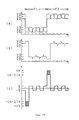
- Fig. 7(a) through (g) The voltage wave applied to the scanning electrodes Y1 through Y6 and the signal electrodes X1 through X6 of the liquid crystal panel 201 when the display pattern is as shown in Fig.6, are shown in Fig. 7(a) through (g) to explain the operation in more detail.
- Fig. 7(a) the full line shows the voltage wave at the signal electrodes X3 and X5 in the positions of the pixels D31 and D51 in Fig. 6.
- the broken line shows the voltage wave at the signal electrodes X2 and X4 in the positions of the pixels D21 and D41.
- Fig. 7(b) the full line shows the voltage wave applied to the scanning electrode Y1, and the broken line shows the noise occurring at the scanning electrode Y1 in the position of the pixel D31.
- Fig. 7(c) shows the voltage wave applied to the scanning electrode Y2 and the noise occurring at this scanning electrode in the position of the pixel D32.
- Figs. 7(d) to (g) show the corresponding voltage waves at the scanning electrodes Y3 to Y6 and the noises occurring at these scanning electrodes in the position of the pixels D33 to D36, respectively.
- the variation of the voltage wave shown by the full line in Fig. 7(a) induces noises in the scanning electrodes Y1, Y2 and Y3 positioned on the upper side of the liquid crystal panel of Fig.
- the variations of the voltage wave at the bottom driven signal electrodes X2 and X4 induce noises in the scanning electrodes Y6, Y5 and Y4 positioned on the lower side of the liquid crystal panel, the noises being strongest in the scanning electrode Y6 and are decreasing in the order of Y6, Y5 and Y4.
- the noises or wave turbulences occurring at the scanning electrodes Y1 through Y6 are compensated for by the Y driver 205 outputting instead of the non-selective voltage the correcting voltage (U) or (L) in a direction opposite to that of the noise.
- the time during which the non-selective voltage is replaced by the correcting voltage is increased or decreased in accordance with the degree of the respective noise in each of the scanning electrodes Y1 through Y6. That is, the correcting voltage is supplied for a long period of time in case of a large noise or turbulence and is supplied for a short period of time in case of a small noise or turbulence.
- the above description of the first embodiment of the invention has been given in connection with a liquid crystal panel in which the signal electrodes X1 through X6 are alternately top and bottom driven, i.e. the odd number signal electrodes are top driven and the even number signal electrodes are bottom driven.
- a possible modification of this first embodiment of the invention is to have all signal electrodes either top driven or bottom driven. Assuming the case of exclusively top driven signal electrodes as an example, the explained first embodiment of the invention could be easily adapted to such case by supplying a signal which is constantly "1" to the gate circuits 402U and 402L in Fig. 4 instead of the output of the T-F/F 401.
- the circuits 402L and 406L through 410L are superfluous in such a case and could either be made inoperative or omitted.
- the circuit 405L would not be necessary in this case and even the circuit 412 could be omitted since the output from the circuit 411L would be always "0".
- the signal voltage wave could be supplied to both ends of each signal electrode according to a second modification of the first embodiment of the present invention.
- ) can be substituted for the function f(k) of the first embodiment.
- the function g(x) is a function which increases as the variable x (x ⁇
- the noise compensation or elimination is performed by using a method for adjusting the correcting amount, in which the difference between the correcting voltage and the non-selective voltage is constant and the time period during which the correcting voltage is applied is increased or decreased depending on the strength of the noise.
- This correction is referred to as "time axis correction”.
- a "voltage axis correction” could be employed by keeping the time period during which the correcting voltage is applied constant and varying the difference between the correcting voltage and the non-selective voltage in accordance with the strength of the noise. It is also possible to vary both, the time of application of the correcting voltage and the voltage itself which would be a "time voltage axis correction". It is also possible to use as the correction voltage a waveform following an exponential function and to vary the wave height in accordance with the required correction amount, and the waveform of a triangle (this is defined as “function waveform correction").
- a second embodiment of the invention will be explained next to show how the unevenness of the display caused by the weft pulling can be avoided.
- the effective voltage applied to a pixel on the scanning electrode is lower than a desired value by a value corresponding to Z'. Therefore, a correction can be carried out by calculating the value Z' for each of the scanning electrodes Y1 through Ys and by correcting the applied voltage in correspondence with the calculated value Z' when the liquid crystal display device is operated.
- Fig. 8 is a block diagram of a second embodiment of the present invention which is based on this principle.
- Numerals 102 and 103 in Fig. 8 designate the control signal and the data signal which correspond to those of the first embodiment so that any further explanation will be omitted here.
- Numeral 801 designates the liquid crystal unit.
- Numeral 804 is a voltage correcting circuit which calculates the value Z' and generates a correcting signal 809 which becomes active during a time period corresponding to the calculated value Z'.
- Numeral 805 is the power source circuit. It supplies Y voltages 806 and X voltages 107 to the liquid crystal unit 801.
- 201 designates the liquid crystal panel which is the same as that of the first embodiment.
- 805 is the scanning electrode driving circuit (referred to as "Y driver” hereinafter) comprising the shift register circuit 206, a switch circuit 911 and a level shifter circuit 912.
- the output terminals of the individual stages of the level shifter circuit 912 are connected to the scanning electrodes Y1 through Y6 of the liquid crystal panel 201, respectively.
- the shift register circuit 206 is the same as that of the first embodiment and, therefore, its explanation is omitted.
- the switch circuit 911 selects one of two groups of voltages which form the Y voltages 806.
- the Y voltages include the voltages V0', V1, V4 and V5' of which V0' and V4 form the first voltage group and V5' and V1 the second voltage group.
- V0' and V4 are the selective voltage and the non-selective voltage, respectively, of the first voltage group.
- V5' and V1 are the selective voltage and the non-selective voltage, respectively, of the second voltage group.
- the voltages of the selected group are supplied by the switch circuit 911 to the level shifter circuit 912.
- the level shifter circuit 912 comprises a number of switches corresponding to the number of scanning electrodes, each switch having two input terminals and one output terminal. Which of the input terminals is connected to the output terminal depends on the state of the control signal applied from the shift register 206 to the respective switch. When the state is “1" each switch selects the selective voltage to apply it to the corresponding one of the scanning electrodes Y1 through Y6. When the state is "0" each switch selects the non-selective voltage and applies this to the respective scanning electrode.
- the signal DIN is taken into the shift register 206 in synchronism with the signal LP and is then successively shifted to each stage of the shift register by the following signals LP.
- the switches of the level shifter circuit 912 are sequentially selected to output the selective voltage while the non-selected switches output the non-selective voltage.
- the signal electrode driving circuit 213 (referred to as "X driver” hereinafter) is the same as that of the first embodiment and, therefore, its explanation is omitted.
- the liquid crystal unit 801 is synchronized with the signals DIN and LP, and the scanning electrodes Y1 through Y6 are sequentially supplied with the selective voltage while the lighting or non-lighting voltage corresponding to the display pattern is applied to the signal electrodes X1 through X6 in synchronism with the selection of the scanning electrodes to display the display pattern on the liquid crystal panel 201.
- the voltage correcting circuit 804 outputs an active correcting signal 809 for a duration corresponding to the value Z' in synchronism with the signal LP when the scanning electrode Yn+1 is selected.
- numeral 1001 designates a counter
- numeral 1002 a function generator circuit
- numeral 1003 a gate circuit
- numeral 1004 an arithmetic circuit
- numeral 1005 a first latch circuit
- numeral 1006 a second latch circuit
- numeral 1007 a correcting signal generator circuit.
- the counter 1001 is reset to 0 by the signal LP and counted up by the signal XSCL.
- the output of the counter 1001 is supplied as an address or as a variable to the function generator circuit 1002.
- the function generator circuit 1002 is provided with a ROM and a diode matrix and outputs predetermined values depending of the count value of the counter 1001.
- the value output by the function generator circuit 1002 corresponds to the function q(i) in the formula (1), i.e. to the weighting function.
- the output of the function generator 1002 increases as the count value of the counter 1001 increases. It should be noted that i corresponds to the count value of the counter 1001 plus 1.
- the gate circuit 1003 generates the logical product of the value output from the function generator circuit 1002 and the data signal 1003. Namely, it outputs the value of the function generator circuit 1002 when the data signal is "1" and outputs 0 when the data signal is "0".
- the gate circuit 1003 thus produces the product q(i) * ⁇ (i) of the formula (1).
- i is the number of trailing edges occurring in the signal XSCL after a trailing edge of the signal LP, and it corresponds to the count value of the counter 1001 plus 1.
- the arithmetic circuit 1004 in synchronism with the signal XSCL, adds the value output from the gate circuit 1003 to the value kept in the first latch circuit 1005 and returns the result into the first latch circuit 1005.
- the first latch circuit 1005 holds the result from the arithmetic circuit 1004.
- the first latch circuit 1005 is reset to 0 by the signal LP.
- the contents of the latch circuit 1005 corresponds to the value Z' of the above formula (1), namely to the number of lighting pixels on the scanning electrode which is to be selected next, each lighting pixel being weighted according to its position on the scanning electrode.
- the first latch circuit Immediately before the first latch circuit is reset at the trailing edge of the signal LP, its contents is taken into the second latch circuit 1006. Since the following scanning electrode is selected at the trailing edge of the signal LP, the value kept by the second latch circuit 1006 corresponds to the weighted number of lighting pixels on the currently selected scanning electrode.
- the correcting signal generator circuit 1007 outputs in synchronism with the signal LP a correcting signal 809 of active "1" during a period of time corresponding to the value kept by the second latch circuit 1006.
- the circuit 1007 comprises for example a counter 1008 which is used to generate a correcting clock signal which may be either the signal XSCL, a signal obtained by dividing or doubling the signal XSCL or another clock signal.
- a counter 1009 is reset to 0 by the signal LP and then counts the correcting clock.
- a coincidence detector circuit 1010 generates the active "1" correcting signal 809 until the count value of the counter 1009 coincides with the value kept by the second latch circuit 1006. It should be noted that the interval of the cycle of the correcting clock is not required to be constant and may be determined by an experiment for example.
- the number of lighting pixels on the scanning electrode to be selected next is counted wherein each lighting pixel is weighted in the manner explained above, and the correcting signal assumes the active state "1" for a period corresponding to the value Z' synchronized with the signal LP by which the next scanning electrode is selected.
- Fig. 11 shows an example of the concrete structure of the power source circuit 805 of Fig. 8.
- 1101 through 1107 designate resistors which are connected in series to form a voltage divider circuit. Voltages V0U and V5L are applied to the two ends of this series connection. Voltages V0, V1, V2, V3, V4 and V5 are derived from the taps of the voltage divider circuit.
- the resistance values of the resistors 1101 through 1107 are selected to fulfil the following conditions:
- 510 in Fig. 11 designates voltage stabilizing circuits which are the same as those of the first embodiment and, thus, will not be further explained.
- Numerals 1108 and 1109 are switch circuits of which the switch circuit 1008 selects the voltage V0U when the correcting signal 809 is “1” and selects the voltage V0 when it is “0” and outputs the selected voltage as voltage V0'. Similarly, the switch 1109 selects the voltage V5L when the correcting signal 809 is “1” and selects the voltage V5 when it is “0” and outputs the selected voltage as voltage V5'.
- the voltages V0U and V5L are the correcting voltages.
- the voltages V0', V4, V5' and V1 are supplied to the liquid crystal unit 801 as the Y voltages 806, and the voltages V0, V2, V3 and V5 are supplied to the liquid crystal unit as the X voltages 107.
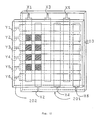
- Figs. 12 and 13 show the liquid crystal panel 201 of Fig. 9 displaying a quadrangle.
- the lighting pixels are hatched and the non-lighting pixels are not hatched.
- the quadrangle is displayed on the left side and in Fig. 13 on the right side.
- the voltage correcting circuit 804 in Fig. 8 counts the number of lighting pixels on each of the scanning electrodes Y1 through Y6 with each lighting pixel being weighted according to its position, to obtain the value Z'.
- Each scanning electrode receives as the selective voltage the correcting voltage V0U and V5L instead of the voltages V0 and V5, respectively, for a period of time which corresponds to the respective value of Z', i.e. as long as the correcting signal 809 is "1".
- the value Z' for the scanning electrodes Y2 through Y5 in case of the display of Fig. 12 is smaller than that in case of the display of Fig. 13. Therefore, under the display in Fig. 12 the time period during which the correcting voltages V0U and V5L are applied as the selective voltage becomes shorter than that in case of the display of Fig. 13, when the scanning electrodes Y2 through Y5 are selected.
- the Y driver 905 sequentially applies the selective voltage to the scanning electrodes Y1 through Y6 while the X driver 213 applies the lighting or the non-lighting voltage to the signal electrodes in accordance with the display pattern.
- a selective voltage having a smaller amount of correction is supplied to the selected scanning electrode in accordance with the fact that the rounding of the voltage wave at the scanning electrode is not so strong when the lighting pixels are positioned near to the driving end of the scanning electrode as is the case with the scanning electrodes Y2 through Y5 in Fig. 12. That is, the correcting voltages V0U and V5L are supplied instead of the voltages V0 and V5, respectively, for a relatively short time only. Contrary, in the example of Fig.
- a selective voltage having a larger amount of correction is supplied to the selected scanning electrode since in this case the rounding of the voltage wave at the scanning electrode is stronger because the lighting pixels are positioned farer away from the driving end of the scanning electrode in case of the scanning electrodes Y2 through Y5.
- the correcting voltages VOU and V5L are supplied instead of the voltages V0 and V5, respectively, for a longer time. The position of lighting pixels can thus be taken into account and compensated for in order to obtain a display without unevenness.
- the second embodiment of the invention has been described in connection with a liquid crystal panel in which the scanning voltage wave is supplied to one end of each scanning electrode.
- the scanning voltage wave can be applied to both ends of each scanning electrode.
- ) must be substituted for the function q(i) for calculating the value Z'.
- the function p(x) is a weighting function which decreases as i (i ⁇
- a time axis correction As a method for adjusting the correction amount in the second embodiment of the invention, it has been described to increase or decrease the time period during which the normal selective voltage is replaced by a predetermined correcting voltage, i.e. a time axis correction has been described. It should be noted that instead of such time axis correction a voltage axis correction, a time voltage axis correction or a function waveform correction could be employed.
- the non-selective voltage is varied, whereas according to the second embodiment and its modifications the selective voltage is varied. Therefore, the two embodiments can be used together in order to achieve optimum results for varyious display patterns.
Landscapes
- Engineering & Computer Science (AREA)
- Physics & Mathematics (AREA)
- Computer Hardware Design (AREA)
- General Physics & Mathematics (AREA)
- Theoretical Computer Science (AREA)
- Chemical & Material Sciences (AREA)
- Crystallography & Structural Chemistry (AREA)
- Liquid Crystal Display Device Control (AREA)
- Liquid Crystal (AREA)
- Control Of Indicators Other Than Cathode Ray Tubes (AREA)
Applications Claiming Priority (2)
| Application Number | Priority Date | Filing Date | Title |
|---|---|---|---|
| JP329055/89 | 1989-12-19 | ||
| JP1329055A JP2867515B2 (ja) | 1989-12-19 | 1989-12-19 | 液晶装置およびその駆動方法 |
Publications (3)
| Publication Number | Publication Date |
|---|---|
| EP0434033A2 true EP0434033A2 (fr) | 1991-06-26 |
| EP0434033A3 EP0434033A3 (en) | 1992-04-22 |
| EP0434033B1 EP0434033B1 (fr) | 1995-08-09 |
Family
ID=18217110
Family Applications (1)
| Application Number | Title | Priority Date | Filing Date |
|---|---|---|---|
| EP90124774A Expired - Lifetime EP0434033B1 (fr) | 1989-12-19 | 1990-12-19 | Dispositif d'affichage à cristaux liquides |
Country Status (5)
| Country | Link |
|---|---|
| EP (1) | EP0434033B1 (fr) |
| JP (1) | JP2867515B2 (fr) |
| KR (1) | KR910013035A (fr) |
| DE (1) | DE69021522T2 (fr) |
| TW (1) | TW201825B (fr) |
Cited By (6)
| Publication number | Priority date | Publication date | Assignee | Title |
|---|---|---|---|---|
| EP0542307A3 (en) * | 1991-11-15 | 1993-08-18 | Asahi Glass Company Ltd. | Image display device and a method of driving the same |
| EP0603713A1 (fr) * | 1992-12-21 | 1994-06-29 | Canon Kabushiki Kaisha | Dispositif d'affichage matriciel |
| US5440322A (en) * | 1993-11-12 | 1995-08-08 | In Focus Systems, Inc. | Passive matrix display having reduced image-degrading crosstalk effects |
| US6580407B1 (en) | 1994-06-08 | 2003-06-17 | Canon Kabushiki Kaisha | Electron-beam generating device having plurality of cold cathode elements, method of driving said device and image forming apparatus applying same |
| US7071635B2 (en) | 2001-09-26 | 2006-07-04 | Sanyo Electric Co., Ltd. | Planar display apparatus |
| FR2916295A1 (fr) * | 2007-05-18 | 2008-11-21 | Nemoptic Sa | Procede d'adressage d'un ecran matriciel a cristal liquide et dispositif appliquant ce procede |
Families Citing this family (1)
| Publication number | Priority date | Publication date | Assignee | Title |
|---|---|---|---|---|
| JP4569133B2 (ja) * | 2004-03-10 | 2010-10-27 | ソニー株式会社 | 電気化学表示装置 |
Family Cites Families (2)
| Publication number | Priority date | Publication date | Assignee | Title |
|---|---|---|---|---|
| JP2906057B2 (ja) * | 1987-08-13 | 1999-06-14 | セイコーエプソン株式会社 | 液晶表示装置 |
| DE3856011T2 (de) * | 1988-06-07 | 1998-03-12 | Sharp Kk | Verfahren und Einrichtung zum Steuern eines kapazitiven Anzeigegeräts |
-
1989
- 1989-12-19 JP JP1329055A patent/JP2867515B2/ja not_active Expired - Fee Related
-
1990
- 1990-10-29 TW TW079109141A patent/TW201825B/zh active
- 1990-12-19 DE DE69021522T patent/DE69021522T2/de not_active Expired - Fee Related
- 1990-12-19 KR KR1019900021012A patent/KR910013035A/ko not_active Withdrawn
- 1990-12-19 EP EP90124774A patent/EP0434033B1/fr not_active Expired - Lifetime
Cited By (9)
| Publication number | Priority date | Publication date | Assignee | Title |
|---|---|---|---|---|
| EP0542307A3 (en) * | 1991-11-15 | 1993-08-18 | Asahi Glass Company Ltd. | Image display device and a method of driving the same |
| EP0603713A1 (fr) * | 1992-12-21 | 1994-06-29 | Canon Kabushiki Kaisha | Dispositif d'affichage matriciel |
| US5657037A (en) * | 1992-12-21 | 1997-08-12 | Canon Kabushiki Kaisha | Display apparatus |
| US5440322A (en) * | 1993-11-12 | 1995-08-08 | In Focus Systems, Inc. | Passive matrix display having reduced image-degrading crosstalk effects |
| US6580407B1 (en) | 1994-06-08 | 2003-06-17 | Canon Kabushiki Kaisha | Electron-beam generating device having plurality of cold cathode elements, method of driving said device and image forming apparatus applying same |
| US7071635B2 (en) | 2001-09-26 | 2006-07-04 | Sanyo Electric Co., Ltd. | Planar display apparatus |
| FR2916295A1 (fr) * | 2007-05-18 | 2008-11-21 | Nemoptic Sa | Procede d'adressage d'un ecran matriciel a cristal liquide et dispositif appliquant ce procede |
| WO2008142301A1 (fr) * | 2007-05-18 | 2008-11-27 | Societe Nemoptic | Procede d'adressage d'un ecran matriciel a cristal liquide et dispositif appliquant ce procede |
| US20100149168A1 (en) * | 2007-05-18 | 2010-06-17 | Patrick Thomas | Method of addressing a liquid crystal matrix screen and device applying this method |
Also Published As
| Publication number | Publication date |
|---|---|
| DE69021522D1 (de) | 1995-09-14 |
| JPH03189621A (ja) | 1991-08-19 |
| EP0434033A3 (en) | 1992-04-22 |
| EP0434033B1 (fr) | 1995-08-09 |
| JP2867515B2 (ja) | 1999-03-08 |
| DE69021522T2 (de) | 1996-02-22 |
| KR910013035A (ko) | 1991-08-08 |
| TW201825B (fr) | 1993-03-11 |
Similar Documents
| Publication | Publication Date | Title |
|---|---|---|
| KR920009028B1 (ko) | 액정 표시 장치 | |
| US5670973A (en) | Method and apparatus for compensating crosstalk in liquid crystal displays | |
| EP0597117B1 (fr) | Unite d'affichage a cristaux liquides et equipement electronique utilisant cette unite | |
| US5179371A (en) | Liquid crystal display device for reducing unevenness of display | |
| US5214417A (en) | Liquid crystal display device | |
| US6806858B2 (en) | Electro-optical apparatus and method of driving electro-optical material, driving circuit therefor, electronic apparatus, and display apparatus | |
| WO1996010245A1 (fr) | Configuration memoire pour informations d'affichage | |
| JPS644197B2 (fr) | ||
| US5119085A (en) | Driving method for a liquid crystal panel | |
| US5184118A (en) | Liquid crystal display apparatus and method of driving same | |
| EP0434033B1 (fr) | Dispositif d'affichage à cristaux liquides | |
| EP0431628B1 (fr) | Dispositif d'affichage à cristaux liquides | |
| JP2993016B2 (ja) | 液晶表示装置及びその駆動方法 | |
| JP2009216813A (ja) | 表示装置 | |
| JP3349626B2 (ja) | 液晶表示装置 | |
| JP3169017B2 (ja) | 液晶表示装置及びその駆動方法 | |
| JP3045099B2 (ja) | 液晶表示装置およびその駆動方法 | |
| JP3045100B2 (ja) | 液晶表示装置およびその駆動方法 | |
| JP3063672B2 (ja) | 液晶表示装置およびその駆動方法 | |
| JP3063671B2 (ja) | 液晶表示装置およびその駆動方法 | |
| JP3291921B2 (ja) | 液晶表示装置 | |
| JP3019035B2 (ja) | 液晶表示装置及びその駆動方法 | |
| JP3050227B2 (ja) | 液晶表示装置及びその駆動方法 | |
| JP3061368B2 (ja) | 液晶表示装置およびその駆動方 | |
| JPH0980375A (ja) | 液晶駆動方法 |
Legal Events
| Date | Code | Title | Description |
|---|---|---|---|
| PUAI | Public reference made under article 153(3) epc to a published international application that has entered the european phase |
Free format text: ORIGINAL CODE: 0009012 |
|
| AK | Designated contracting states |
Kind code of ref document: A2 Designated state(s): CH DE FR GB LI |
|
| PUAL | Search report despatched |
Free format text: ORIGINAL CODE: 0009013 |
|
| AK | Designated contracting states |
Kind code of ref document: A3 Designated state(s): CH DE FR GB LI |
|
| 17P | Request for examination filed |
Effective date: 19921002 |
|
| 17Q | First examination report despatched |
Effective date: 19940203 |
|
| GRAA | (expected) grant |
Free format text: ORIGINAL CODE: 0009210 |
|
| AK | Designated contracting states |
Kind code of ref document: B1 Designated state(s): CH DE FR GB LI |
|
| REF | Corresponds to: |
Ref document number: 69021522 Country of ref document: DE Date of ref document: 19950914 |
|
| ET | Fr: translation filed | ||
| PLBE | No opposition filed within time limit |
Free format text: ORIGINAL CODE: 0009261 |
|
| STAA | Information on the status of an ep patent application or granted ep patent |
Free format text: STATUS: NO OPPOSITION FILED WITHIN TIME LIMIT |
|
| 26N | No opposition filed | ||
| REG | Reference to a national code |
Ref country code: GB Ref legal event code: IF02 |
|
| REG | Reference to a national code |
Ref country code: CH Ref legal event code: PFA Owner name: SEIKO EPSON CORPORATION Free format text: SEIKO EPSON CORPORATION#4-1, NISHISHINJUKU 2-CHOME#SHINJUKU-KU/TOKYO-TO (JP) -TRANSFER TO- SEIKO EPSON CORPORATION#4-1, NISHISHINJUKU 2-CHOME#SHINJUKU-KU/TOKYO-TO (JP) |
|
| PGFP | Annual fee paid to national office [announced via postgrant information from national office to epo] |
Ref country code: CH Payment date: 20071213 Year of fee payment: 18 |
|
| PGFP | Annual fee paid to national office [announced via postgrant information from national office to epo] |
Ref country code: FR Payment date: 20071210 Year of fee payment: 18 Ref country code: GB Payment date: 20071219 Year of fee payment: 18 |
|
| PGFP | Annual fee paid to national office [announced via postgrant information from national office to epo] |
Ref country code: DE Payment date: 20071213 Year of fee payment: 18 |
|
| REG | Reference to a national code |
Ref country code: CH Ref legal event code: PL |
|
| GBPC | Gb: european patent ceased through non-payment of renewal fee |
Effective date: 20081219 |
|
| REG | Reference to a national code |
Ref country code: FR Ref legal event code: ST Effective date: 20090831 |
|
| PG25 | Lapsed in a contracting state [announced via postgrant information from national office to epo] |
Ref country code: LI Free format text: LAPSE BECAUSE OF NON-PAYMENT OF DUE FEES Effective date: 20081231 Ref country code: CH Free format text: LAPSE BECAUSE OF NON-PAYMENT OF DUE FEES Effective date: 20081231 Ref country code: DE Free format text: LAPSE BECAUSE OF NON-PAYMENT OF DUE FEES Effective date: 20090701 |
|
| PG25 | Lapsed in a contracting state [announced via postgrant information from national office to epo] |
Ref country code: GB Free format text: LAPSE BECAUSE OF NON-PAYMENT OF DUE FEES Effective date: 20081219 |
|
| PG25 | Lapsed in a contracting state [announced via postgrant information from national office to epo] |
Ref country code: FR Free format text: LAPSE BECAUSE OF NON-PAYMENT OF DUE FEES Effective date: 20081231 |