EP0434192A2 - Carte de base de rattrapage - Google Patents
Carte de base de rattrapage Download PDFInfo
- Publication number
- EP0434192A2 EP0434192A2 EP90311406A EP90311406A EP0434192A2 EP 0434192 A2 EP0434192 A2 EP 0434192A2 EP 90311406 A EP90311406 A EP 90311406A EP 90311406 A EP90311406 A EP 90311406A EP 0434192 A2 EP0434192 A2 EP 0434192A2
- Authority
- EP
- European Patent Office
- Prior art keywords
- card
- base
- daughter
- connector
- circuit card
- Prior art date
- Legal status (The legal status is an assumption and is not a legal conclusion. Google has not performed a legal analysis and makes no representation as to the accuracy of the status listed.)
- Granted
Links
Images


Classifications
-
- H—ELECTRICITY
- H05—ELECTRIC TECHNIQUES NOT OTHERWISE PROVIDED FOR
- H05K—PRINTED CIRCUITS; CASINGS OR CONSTRUCTIONAL DETAILS OF ELECTRIC APPARATUS; MANUFACTURE OF ASSEMBLAGES OF ELECTRICAL COMPONENTS
- H05K7/00—Constructional details common to different types of electric apparatus
- H05K7/14—Mounting supporting structure in casing or on frame or rack
- H05K7/1461—Slidable card holders; Card stiffeners; Control or display means therefor
-
- G—PHYSICS
- G06—COMPUTING OR CALCULATING; COUNTING
- G06F—ELECTRIC DIGITAL DATA PROCESSING
- G06F1/00—Details not covered by groups G06F3/00 - G06F13/00 and G06F21/00
- G06F1/16—Constructional details or arrangements
- G06F1/18—Packaging or power distribution
Definitions
- the present invention relates to a printed circuit card for a computer system.
- the present invention relates to a printed circuit card which can attach to a daughter card designed for a system with a different architecture, and which can attach to a daughter card with an integral I/O connector without violating the space envelope of any adjacent printed circuit card.
- printed circuit cards are used to carry the bulk of the electronic circuitry.
- a common design has a large printed circuit card carrying the circuitry for operating the basic functions of the computer. This large printed circuit card will be referred to hereinafter as a mother board.
- Base cards are printed circuit boards which are designed to hold electronic circuitry required to perform a specific function, such as controlling a printer or storage device and interfacing that device with the mother board, or any other desired function.
- the specific function performed is not important for the purposes of this disclosure.
- the advantage of using base cards is that it requires the cost of circuitry to be incurred only when it is required to support a specific function.
- Base cards typically have edge connectors with electrical contacts which can be plugged into a connector on the mother board, thereby adding the base card circuitry to the circuitry on the mother board.
- base cards which connect to I/O devices usually have an I/O connector on an edge of the board which allows a cable to be connected between the I/O device and the base card.
- the mother board has multiple connectors to attach to multiple base cards. While the plane of the base card is often perpendicular to the plane of the mother board, it is not required to be perpendicular, and may in fact be oriented at any angle convenient for packaging purposes.
- a daughter card is defined for the purposes of this disclosure as a printed circuit board which connects to a base card and adds circuitry to the base card in the same manner as the base card adds circuitry to the mother board. It is typically attached to the base card in a plane which is substantially parallel to the plane of the base card.
- more than one type of daughter card may be designed for a base card, just as more than one type of base card may be designed for a mother board.
- the use of multiple base cards by a mother board has imposed space constrains.
- the space constraints result in a defined physical space envelope in which each base card may be placed.
- an additional limitation on the location of the I/O connector is created which requires that the connector be attached to the base card. This is due to the thickness of the I/O connector which, if placed on the daughter card, would impinge on the space envelope of the next base card.
- the limitation on the location of the I/O connector requires the use of a connector which can be used by any of the daughter cards which might be connected to the base card. It is possible that each of the multiple optional daughter cards available for a given base card may have a different I/O connector requirement due to the number of connection lines required for the particular I/O device. This generally results in the selection of the I/O connector with the largest number of lines, and hence, the I/O connector with the highest cost.
- An aim of the present invention is to provide a base card having a connector for connecting to a daughter card without violating a physical space envelope of the base card.
- a base circuit card assembly comprising a base circuit card carrying an edge connector for electrically connecting the base circuit card to a mother board and at least one base card connector for electrically attaching a daughter circuit card to the base circuit card; characterised in that the edge connector is offset to one side of the base circuit card to permit attachment of the daughter circuit card to the base circuit card without violating an envelope of space defined by the base circuit card assembly.
- a base circuit board assembly for mounting on a mother board, comprising: a base circuit board, the base circuit board further comprising: an edge connector for electrical attachment of the base circuit board to a mother board, an offset for positioning the base circuit board such that it is offset to one side of the edge connector, at least one base card connector for electrically attaching a daughter circuit board to the base circuit board; whereby, daughter circuit cards can attach to the base circuit board without violating the space envelope of the base circuit board.
- a base card having an offset edge connector, such that the edge connector occupies one plane and the base card occupies a parallel plane.
- the base card comprises an I/O connector designed for a specific daughter card.
- the base card enables daughter cards developed for one architecture type to be used in a system based on a different architecture type.
- Figure 1 is an isometric view of the base card with offset edge connector.
- Figure 2 is an end view of the base card looking into the plane of the board
- Figure 3 is a side view of a daughter card.
- Figure 4 is an edge view of a daughter card.
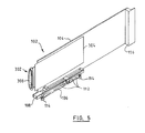
- Figure 5 is an isometric view of the base card with and attached daughter card.
- the problems discussed above relating to incompatibility of cards between differing architecture types and space envelope problems caused by placing I/O connectors on daughter cards, is overcome by modifying the base card on one of the system types such that a daughter card can fit within the space envelope of the base card. This is accomplished by offsetting the base card from its edge connector. By offsetting the base card, a daughter card designed for another architecture can fit in the packaging structure of the present system, thereby allowing migration of daughter cards between different packaging architecture types.
- the daughter card can have an integral I/O connector without violating the space envelope of the base card, thereby eliminating the need for a more expensive I/O connector on the base card.
- Figure 1 shows an embodiment of the base card 102.
- the printed circuit 104 is shown as a blank board for ease of illustration.
- the specific circuitry used on the base card 102 is not shown because it will vary depending on the type of I/O device or function and is not necessary to understanding the invention.
- Electrical connections 110 are shown to illustrate the location where the daughter card (shown in figures 3-5) would attach electrically to the base card 102 in the preferred embodiment. Those skilled in the art will realise that the location of the electrical connections 110 is an arbitrary design choice. In practice, a male or female connector can be attached to the printed circuit 104 via electrical connections 110 for mating with a female or male connector, respectively, on the daughter card (not shown).
- the daughter card it is also possible to permanently attach the daughter card to the base card 102 via permanent electrical wire connection.
- detachable electrical connectors would be used in the preferred embodiment to facilitate ease of removal or substitution of the daughter card.
- the specific mating connectors used are a mere design choice based on the requirements of the particular circuit used by the printed circuit 104 and can be chosen from numerous commercially available connectors.
- the edge connector 106 is separated from the printed circuit 104 by an offset 108.
- the edge connector 106 is shown to be in a substantially parallel plane with the printed circuit board 104 in the preferred embodiment. However, those skilled in the art will understand that the invention can be implemented with the plane of the printed circuit 104 at an angle to the plane of the edge connector 106.
- the specific offset distance provided by the offset 108 will be a design choice based on several factors, such as space envelope limitations, circuit component types, etc. In prior art adapter boards, well known in the art, the printed circuit 104 and the edge connector 106 would typically be a single element sharing the same plane.
- the preferred embodiment shown in figure 1 offsets the printed circuit 104 to allow use of the plane space above the edge connector 106 by a daughter card.
- the conductive pads 114 provide for electrical connection to the mother board (not shown) when inserted into a connector on the mother board.
- Lines 112 provide electrical connection between the edge connector and printed circuit 104. Lines 112 run through offset 108. Lines 112 connect to conductive pads 114 to provide signal paths between the mother board and printed circuit 104.
- the edge connector 106 is shown in two sections for illustrative purposes. However, mere design choices based on the particular mother board and base card in question will determine the actual configuration in practice.
- Figure 1 also shows support tab 116.
- Support tab 116 is inserted in supports commonly found in micro-computers to hold the end of a base card in place. This type of physical support method is well known in the art. As shown, the support tab 116 is offset the same distance as the edge connector 106. This allows the support tab 116 to be in the same plane as the edge connector 106, which in turn allows the base card 102 to be inserted in the micro-computer without relocating the supports. It will be understood by those skilled in the art that the support tab is an optional feature because the base card 102 for a particular function can be a short card which does not extend to the end of its board slot.
- Figure 2 shows an end view of the base card described above in the discussion of figure 1.
- mounting screws 202 which provide the physical connection of the edge connector 106, the printed circuit 104 and the offset 108 are shown.
- Support tab 116 is shown aligned in the same plane as the edge connector 106.
- FIG. 3 shows a side view of a daughter card 302.
- the circuit components will vary for the same reasons that the circuit components on the printed circuit 104, discussed above, will vary and are, therefore, not shown.
- Daughter board 302 shows daughter circuit 304 which would, in practice, have the circuitry for the daughter card function mounted thereon.
- Mounting screws 306 show a typical method of physically attaching the daughter card 302 to the base card 102. It is understood that the actual method of physical attachment and the location of the attaching points are a mere design choice.
- I/O connector 308 At the left end of daughter card 302 is I/O connector 308. The particular I/O connector used will also vary based on the function of the daughter card 302.
- Figure 4 shows a top view of the daughter card 302. Mounting screws 306 are shown contained in spacers 402. I/O connector 308 is shown at the left end of daughter card 302. Electrical connections 404 are shown to illustrate one type of electrical connection for providing signal connection between the daughter card 302 and the base card 102.
- Figure 5 shows the position a daughter card 302 would occupy in relation to a printed circuit 104, and an edge connector 106 on a base card 102.
- the daughter card 302 is generally within the plane occupied by the edge connector 106 and in a plane parallel to that occupied by the printed circuit 104.
- an I/O adapter 308 specifically designed to meet the requirements of the daughter card 302 can be directly attached to the daughter card 302 without violating the envelope space of the base card 102.
- the requirement for a general purpose I/O connector 308 on the base card 102 is eliminated, allowing the least cost I/O connector 308 to be selected for the base card 102 / daughter card 302 combination.
- the offset base card 102 allows more flexibility in physically locating a daughter card 302 in a space envelope. This allows daughter cards 302, which would not normally fit in a given packaging architecture to be used without modification. As a result, daughter cards can be migrated from one architecture type to another.
- the plane used by the daughter card can vary from the plane used by the edge connector without violating the space envelope.
- the base card plane and daughter card plane be parallel. Accordingly, the invention herein disclosed is to be limited only as specified in the following claims.
Landscapes
- Engineering & Computer Science (AREA)
- Theoretical Computer Science (AREA)
- Microelectronics & Electronic Packaging (AREA)
- Power Engineering (AREA)
- Human Computer Interaction (AREA)
- Physics & Mathematics (AREA)
- General Engineering & Computer Science (AREA)
- General Physics & Mathematics (AREA)
- Combinations Of Printed Boards (AREA)
- Mounting Of Printed Circuit Boards And The Like (AREA)
Applications Claiming Priority (2)
| Application Number | Priority Date | Filing Date | Title |
|---|---|---|---|
| US426611 | 1982-09-29 | ||
| US07/426,611 US5099394A (en) | 1989-10-24 | 1989-10-24 | Offset basecard |
Publications (3)
| Publication Number | Publication Date |
|---|---|
| EP0434192A2 true EP0434192A2 (fr) | 1991-06-26 |
| EP0434192A3 EP0434192A3 (en) | 1992-07-08 |
| EP0434192B1 EP0434192B1 (fr) | 1995-01-04 |
Family
ID=23691492
Family Applications (1)
| Application Number | Title | Priority Date | Filing Date |
|---|---|---|---|
| EP90311406A Expired - Lifetime EP0434192B1 (fr) | 1989-10-24 | 1990-10-17 | Carte de base de rattrapage |
Country Status (4)
| Country | Link |
|---|---|
| US (1) | US5099394A (fr) |
| EP (1) | EP0434192B1 (fr) |
| JP (1) | JP2502183B2 (fr) |
| DE (1) | DE69015792T2 (fr) |
Cited By (4)
| Publication number | Priority date | Publication date | Assignee | Title |
|---|---|---|---|---|
| ES2065280A2 (es) * | 1993-06-25 | 1995-02-01 | Avacon Sa | Sistema electromecanico de normalizacion de placas electronicas no normalizadas. |
| EP0704820A1 (fr) * | 1994-09-22 | 1996-04-03 | Yamaichi Electronics Co., Ltd. | Carte mémoire |
| DE29617034U1 (de) * | 1996-09-30 | 1996-12-05 | Stocko Metallwarenfabriken Henkels & Sohn GmbH & Co, 42327 Wuppertal | PC-Card Adapter |
| EP1722617A1 (fr) * | 2005-05-12 | 2006-11-15 | Harman Becker Automotive Systems GmbH | Dispositif électronique |
Families Citing this family (20)
| Publication number | Priority date | Publication date | Assignee | Title |
|---|---|---|---|---|
| US5663901A (en) | 1991-04-11 | 1997-09-02 | Sandisk Corporation | Computer memory cards using flash EEPROM integrated circuit chips and memory-controller systems |
| US5214570A (en) * | 1992-04-03 | 1993-05-25 | Clearpoint Research Corporation | Compact memory module |
| USD354271S (en) | 1993-05-17 | 1995-01-10 | 3 Com Corporation | Fiber optic interchangeable transceiver module |
| USD354732S (en) | 1993-05-17 | 1995-01-24 | 3Com Corporation | Fiber optic interchangeable transceiver module |
| USD353799S (en) | 1993-05-17 | 1994-12-27 | 3 Com Corporation | Network adapter card for interchangeable transceiver modules |
| USD354940S (en) | 1993-05-17 | 1995-01-31 | 3 Com Corporation | RJ-45 interchangeable transceiver module |
| USD353796S (en) | 1993-05-17 | 1994-12-27 | 3 Com Corporation | Fiber optic interchangeable transceiver module |
| US7137011B1 (en) | 1993-09-01 | 2006-11-14 | Sandisk Corporation | Removable mother/daughter peripheral card |
| US5887145A (en) * | 1993-09-01 | 1999-03-23 | Sandisk Corporation | Removable mother/daughter peripheral card |
| US5611057A (en) * | 1994-10-06 | 1997-03-11 | Dell Usa, L.P. | Computer system modular add-in daughter card for an adapter card which also functions as an independent add-in card |
| US5628637A (en) * | 1994-12-08 | 1997-05-13 | Dell Usa, L.P. | Computer system SCSI adapter card including an add-in daughter board providing an external SCSI connector for modular and upgradable SCSI bus routing options |
| US6256208B1 (en) * | 1998-10-07 | 2001-07-03 | Ati Technologies, Inc. | Adaptable expansion card with a multi-position daughter card and method therefore |
| US6146150A (en) * | 1998-11-24 | 2000-11-14 | International Business Machines Corporation | Circuit card with separate interfaces for different bus architectures |
| US6328598B1 (en) * | 2000-04-21 | 2001-12-11 | International Business Machines Corporation | Printed circuit board supporting different types of chassis connector panels |
| US6570775B2 (en) * | 2001-09-20 | 2003-05-27 | Global Sun Technology Inc. | Circuit board assembly having a compact structure |
| US20030135470A1 (en) * | 2002-01-16 | 2003-07-17 | Beard Robert E. | Method and system for credit card purchases |
| US20060206677A1 (en) * | 2003-07-03 | 2006-09-14 | Electronics And Telecommunications Research Institute | System and method of an efficient snapshot for shared large storage |
| JP5435561B2 (ja) | 2009-10-21 | 2014-03-05 | 日立マクセル株式会社 | 回転刃、および回転刃を有する小型電気機器 |
| US9274548B2 (en) * | 2013-03-01 | 2016-03-01 | Seagate Technology Llc | Electronic apparatus comprising backplane and methods of assembling and disassembling |
| TWI645623B (zh) * | 2017-09-30 | 2018-12-21 | 慧榮科技股份有限公司 | 記憶裝置 |
Family Cites Families (13)
| Publication number | Priority date | Publication date | Assignee | Title |
|---|---|---|---|---|
| US3300686A (en) * | 1963-07-30 | 1967-01-24 | Ibm | Compatible packaging of miniaturized circuit modules |
| FR2374820A1 (fr) * | 1976-12-16 | 1978-07-13 | Itt Produits Ind | Systeme d'accouplement mecanique et electrique entre un organe amovible et une structure fixe |
| US4550362A (en) * | 1982-11-22 | 1985-10-29 | Gte Automatic Electric Inc. | Board positioning arrangement |
| DE8308866U1 (de) * | 1983-03-24 | 1985-05-02 | Siemens AG, 1000 Berlin und 8000 München | Flachbaugruppe |
| US4511950A (en) * | 1983-06-27 | 1985-04-16 | Northern Telecom Limited | Backpanel assemblies |
| US4683550A (en) * | 1984-07-30 | 1987-07-28 | Burr-Brown Corporation | Personal computer instrumentation system including carrier board having bus-oriented plug-in instrumentation modules |
| GB2163305B (en) * | 1984-08-17 | 1988-11-02 | Teradyne Inc | Backplane connector |
| JPS62202596A (ja) * | 1986-02-28 | 1987-09-07 | シャープ株式会社 | メモリ基板装置 |
| JPS62188189U (fr) * | 1986-05-21 | 1987-11-30 | ||
| US4834660A (en) * | 1987-06-03 | 1989-05-30 | Harris Corporation | Flexible zero insertion force interconnector between circuit boards |
| US4899254A (en) * | 1987-07-22 | 1990-02-06 | Tandem Computers Incorporated | Electronic module interconnection system |
| US4840570A (en) * | 1988-06-27 | 1989-06-20 | Teknekron Infoswitch Corporation | Plug-in card module |
| US4924355A (en) * | 1989-04-25 | 1990-05-08 | Dell Corporate Services Corporation | Personal computer having expansion card adapter bracket |
-
1989
- 1989-10-24 US US07/426,611 patent/US5099394A/en not_active Expired - Fee Related
-
1990
- 1990-10-05 JP JP2266600A patent/JP2502183B2/ja not_active Expired - Lifetime
- 1990-10-17 EP EP90311406A patent/EP0434192B1/fr not_active Expired - Lifetime
- 1990-10-17 DE DE69015792T patent/DE69015792T2/de not_active Expired - Fee Related
Cited By (6)
| Publication number | Priority date | Publication date | Assignee | Title |
|---|---|---|---|---|
| ES2065280A2 (es) * | 1993-06-25 | 1995-02-01 | Avacon Sa | Sistema electromecanico de normalizacion de placas electronicas no normalizadas. |
| EP0704820A1 (fr) * | 1994-09-22 | 1996-04-03 | Yamaichi Electronics Co., Ltd. | Carte mémoire |
| DE29617034U1 (de) * | 1996-09-30 | 1996-12-05 | Stocko Metallwarenfabriken Henkels & Sohn GmbH & Co, 42327 Wuppertal | PC-Card Adapter |
| US6176724B1 (en) | 1996-09-30 | 2001-01-23 | Stocko Metallwarenfabriken Henkels Und Sohn | PC card adapter |
| EP1722617A1 (fr) * | 2005-05-12 | 2006-11-15 | Harman Becker Automotive Systems GmbH | Dispositif électronique |
| US8208263B2 (en) | 2005-05-12 | 2012-06-26 | Harman Becker Automotive Systems Gmbh | Electronic device |
Also Published As
| Publication number | Publication date |
|---|---|
| EP0434192B1 (fr) | 1995-01-04 |
| DE69015792T2 (de) | 1995-06-29 |
| EP0434192A3 (en) | 1992-07-08 |
| JPH03148198A (ja) | 1991-06-24 |
| US5099394A (en) | 1992-03-24 |
| DE69015792D1 (de) | 1995-02-16 |
| JP2502183B2 (ja) | 1996-05-29 |
Similar Documents
| Publication | Publication Date | Title |
|---|---|---|
| EP0434192B1 (fr) | Carte de base de rattrapage | |
| CA1327410C (fr) | Carte et circuit d'adaptation de peripheriques utilisables avec deux architectures d'ordinateur personnel | |
| US6215656B1 (en) | Method and apparatus for factory or user configurable external connectors | |
| US5576935A (en) | Common circuit board connectable to multiple alternative single-sided expansion boards | |
| US5544008A (en) | Computer expansion module apparatus | |
| US5628637A (en) | Computer system SCSI adapter card including an add-in daughter board providing an external SCSI connector for modular and upgradable SCSI bus routing options | |
| US6494749B1 (en) | Connector with mounting fixture for removable storage device | |
| US4936785A (en) | Interchangeable adapter module for electronic devices | |
| US5214567A (en) | Modular peripheral platform having two disk drives and one electrical connector | |
| US5604871A (en) | Modular host local expansion upgrade | |
| US5040993A (en) | Interchangeable adapter module for electronic devices | |
| US7362589B2 (en) | Circuit board adapted to couple to different types of add-in cards | |
| CA2016546A1 (fr) | Carte de memoire modulaire pour ordinateur | |
| US5077683A (en) | Expansion slot adapter with embedded data device interface | |
| US5721673A (en) | Socket for retaining multiple electronic packages | |
| US6313984B1 (en) | Low profile hard disk drive assembly mounting to computer motherboard | |
| WO2002044913A2 (fr) | Topologie pour systeme de carte adaptatrice de connexion de bus pci de 66 mhz | |
| EP0815709B1 (fr) | Ensemble carte mère possédant une prise unique pouvant accepter un ou plusieurs boîtiers de circuits intégrés | |
| US5973924A (en) | Symmetric multi-processor-package design | |
| US20030049948A1 (en) | Apparatus and method for coupling buses | |
| US6662255B1 (en) | System for housing CompactPCI adapters in a non-CompactPCI frame | |
| US5987553A (en) | Adaptor board interconnection for a processor board and motherboard | |
| US5237131A (en) | Printed circuit board design for multiple versions of integrated circuit device | |
| JP2002314215A (ja) | プリント基板装置 | |
| US6288908B1 (en) | Peripheral apparatus for PC cards |
Legal Events
| Date | Code | Title | Description |
|---|---|---|---|
| PUAI | Public reference made under article 153(3) epc to a published international application that has entered the european phase |
Free format text: ORIGINAL CODE: 0009012 |
|
| 17P | Request for examination filed |
Effective date: 19901213 |
|
| AK | Designated contracting states |
Kind code of ref document: A2 Designated state(s): DE FR GB |
|
| PUAL | Search report despatched |
Free format text: ORIGINAL CODE: 0009013 |
|
| AK | Designated contracting states |
Kind code of ref document: A3 Designated state(s): DE FR GB |
|
| 17Q | First examination report despatched |
Effective date: 19930429 |
|
| GRAA | (expected) grant |
Free format text: ORIGINAL CODE: 0009210 |
|
| AK | Designated contracting states |
Kind code of ref document: B1 Designated state(s): DE FR GB |
|
| REF | Corresponds to: |
Ref document number: 69015792 Country of ref document: DE Date of ref document: 19950216 |
|
| ET | Fr: translation filed | ||
| PGFP | Annual fee paid to national office [announced via postgrant information from national office to epo] |
Ref country code: FR Payment date: 19951009 Year of fee payment: 6 |
|
| PGFP | Annual fee paid to national office [announced via postgrant information from national office to epo] |
Ref country code: DE Payment date: 19951030 Year of fee payment: 6 |
|
| PLBE | No opposition filed within time limit |
Free format text: ORIGINAL CODE: 0009261 |
|
| STAA | Information on the status of an ep patent application or granted ep patent |
Free format text: STATUS: NO OPPOSITION FILED WITHIN TIME LIMIT |
|
| 26N | No opposition filed | ||
| PG25 | Lapsed in a contracting state [announced via postgrant information from national office to epo] |
Ref country code: FR Effective date: 19970630 |
|
| PG25 | Lapsed in a contracting state [announced via postgrant information from national office to epo] |
Ref country code: DE Effective date: 19970701 |
|
| REG | Reference to a national code |
Ref country code: FR Ref legal event code: ST |
|
| PGFP | Annual fee paid to national office [announced via postgrant information from national office to epo] |
Ref country code: GB Payment date: 19970923 Year of fee payment: 8 |
|
| PG25 | Lapsed in a contracting state [announced via postgrant information from national office to epo] |
Ref country code: GB Free format text: LAPSE BECAUSE OF NON-PAYMENT OF DUE FEES Effective date: 19981017 |
|
| GBPC | Gb: european patent ceased through non-payment of renewal fee |
Effective date: 19981017 |