EP0434465A2 - Treiberschaltung für ein Flüssigkristallanzeigegerät - Google Patents
Treiberschaltung für ein Flüssigkristallanzeigegerät Download PDFInfo
- Publication number
- EP0434465A2 EP0434465A2 EP90314190A EP90314190A EP0434465A2 EP 0434465 A2 EP0434465 A2 EP 0434465A2 EP 90314190 A EP90314190 A EP 90314190A EP 90314190 A EP90314190 A EP 90314190A EP 0434465 A2 EP0434465 A2 EP 0434465A2
- Authority
- EP
- European Patent Office
- Prior art keywords
- polarity
- input
- linear
- output characteristics
- driving circuit
- Prior art date
- Legal status (The legal status is an assumption and is not a legal conclusion. Google has not performed a legal analysis and makes no representation as to the accuracy of the status listed.)
- Granted
Links
Images




Classifications
-
- G—PHYSICS
- G09—EDUCATION; CRYPTOGRAPHY; DISPLAY; ADVERTISING; SEALS
- G09G—ARRANGEMENTS OR CIRCUITS FOR CONTROL OF INDICATING DEVICES USING STATIC MEANS TO PRESENT VARIABLE INFORMATION
- G09G3/00—Control arrangements or circuits, of interest only in connection with visual indicators other than cathode-ray tubes
- G09G3/20—Control arrangements or circuits, of interest only in connection with visual indicators other than cathode-ray tubes for presentation of an assembly of a number of characters, e.g. a page, by composing the assembly by combination of individual elements arranged in a matrix no fixed position being assigned to or needed to be assigned to the individual characters or partial characters
- G09G3/34—Control arrangements or circuits, of interest only in connection with visual indicators other than cathode-ray tubes for presentation of an assembly of a number of characters, e.g. a page, by composing the assembly by combination of individual elements arranged in a matrix no fixed position being assigned to or needed to be assigned to the individual characters or partial characters by control of light from an independent source
- G09G3/36—Control arrangements or circuits, of interest only in connection with visual indicators other than cathode-ray tubes for presentation of an assembly of a number of characters, e.g. a page, by composing the assembly by combination of individual elements arranged in a matrix no fixed position being assigned to or needed to be assigned to the individual characters or partial characters by control of light from an independent source using liquid crystals
- G09G3/3611—Control of matrices with row and column drivers
- G09G3/3614—Control of polarity reversal in general
Definitions
- This invention relates to a driving circuit for a liquid crystal display apparatus, and more particularly to a driving circuit for a liquid crystal display apparatus in which thin film transistors are used as switching elements.
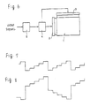
- FIG. 6 shows a driving circuit for driving an active matrix type LCD apparatus 1 in which thin film transistors (TFTs) are arranged as switching elements in a matrix form.
- the driving circuit shown in Figure 6 comprises a source driver 2, a data driver 3, a controller 4, and a polarity-inverting circuit 5.
- a DC voltage is applied to the liquid crystal in the LCD apparatus 1
- electrochemical reaction occurs in the liquid crystal, thereby deteriorating the liquid crystal.
- the driving circuit is provided with the polarity-inverting circuit 5 so that the LCD apparatus 1 is AC-driven.
- the polarity-inverting circuit 5 generally comprises an amplifier, an inverter which inverts the polarity of the output of the amplifier, and a switching circuit which alternatingly selects either of the outputs of the amplifier and inverter to output the selected output.
- the polarity-inverting circuit 5 converts input video signals into polarity-inverted signals (AC signals).
- Figure 7 shows gray scale video signals.
- the polarity-inverting circuit 5 converts the video signals of Figure 7 into polarity-inverted signals shown in Figure 8.
- the pattern is "memorized" in the liquid crystal, with the result in that some extent of time is required to completely distinguish this memorized pattern. Even when another pattern is to be displayed, therefore, this memorized pattern also appears as a residual image on the apparatus 1 (i.e., the residual image phenomenon occurs). This residual image phenomenon greatly impairs the image quality.
- the driving circuit of this invention which overcomes the above-discussed and numerous other disadvantages and deficiencies of the prior art, comprises a polarity-inverting circuit for converting input video signals into polarity-alternating signals, and said polarity-inverting circuit has the input-output characteristics which are at least partially non-linaer.
- the polarity-inverting circuit has input-output characteristics which are linear in the positive region, and non-linear in the negative region.
- the polarity-inverting circuit may have input-output characteristics which are non-linear in the positive region, and linear in the negative region.
- Figure 10 shows an equivalent circuit of a picture element (pixel) of the LCD apparatus 1 ( Figure 6). Each pixel is provided with a TFT 13.
- Figure 11 shows the sectional structure of the TFT 13.
- the source electrode 13s and drain electrode 13d of the TFT 13 are connected to a source line 11 and a pixel electrode 14, respectively.
- a gate line 12 which perpendicularly intersects the source line 11 functions also as the gate electrode of the TFT 13.
- the numerals 18 and 19 in Figure 11 indicate a gate insulating film, and a semiconductor film, respectively.
- a parasitic capacitance C gd is formed between the gate line 12 and the drain electrode 13d
- a pixel capacitance C LC is formed between the pixel electrode 14 and a counter electrode 17 which is opposite to the pixel electrode 14.
- V ON indicates the ON-voltage at which the TFT 13 is On
- V OFF the OFF-voltage at which the TFT 13 is OFF.
- the level of the gate signal i.e., the gate voltage
- T1 the level of the gate signal
- the level of the gate signal is changed from V OFF to V ON at time T1
- the TFT 13 turns ON and the potential of the drain electrode 13d and pixel electrode 14 begins to increase towards the voltage level applied to the source line 11. In this way, the "writing" of the pixel is performed.
- the level of the gate signal is reduced from V ON to V OFF , thereby turning OFF the TFT 13.
- the potential of the counter electrode 17 remains unchanged.
- the potential of the drain electrode 13d and pixel electrode 14 (hereinafter, referred to as "the drain potential") is shifted by This drain potential which has been shifted by ⁇ V is maintained until the next writing (i.e., between times T2 and T3).
- the drain potential is offset by ⁇ V with respect to the signal applied to the source line 11.
- the offset voltage ⁇ V which is caused by the parasitic capacitance C gd of the TFT 13 is changed in a large degree (in the above example, as much as about 1.5 V) in accordance with the contents of images to be displayed.
- offset voltages ⁇ V of different levels are applied to each pixel according to the respective contents of the pattern to be displayed therein.
- DC voltages of different levels are applied to respective pixels for a long period of time.
- This prolonged application of DC voltages causes elechtrochemical changes in the components of each pixel (the liquid crystal, the orientation film, the protection film, etc.). These changes are memorized in the respective pixel of the LCD apparatus 1.
- the residual image phenomenon is caused by the fact that the levels of offset voltages ⁇ V change in accordance with the contents of patterns to be displayed. Hence, if the changes of offset voltages ⁇ V can be corrected or compensated, the problem of the residual image phenomenon will be solved.
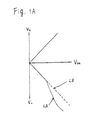
- Figure 1A shows the input-output characteristics of a polarity-inverting circuit used in a driving circuit according to the invention.
- the solid line LA indicates the input-output characteristics of the embodiment, and the broken line LB that of the prior art.
- the driving circuit according to the invention may be generally constructed in the same manner as that of the prior art shown in Figure 6.
- the polarity-inverting circuit 5 is constructed so that the input-output characteristics in the positive region are linear in a manner similar to that of the prior art, and that the input-output characteristics in the negative region are non-linear unlike that of the prior art (in which the input-output characteristics in both the positive and negative regions are linear).
- the non-linear characteristics provide an input/output relationship that, even when inputs of the same level are respectively supplied to the embodiment and to a circuit of the prior art, the output level of the embodiment is smaller than that of the prior art circuit, thereby correcting or compensating changes of the offset voltages ⁇ V.
- the drain potential (DC level) is substantially constant irrespective of the contents of patterns to be displayed.
- the DC level of signals output from the polarity-inverting circuit 5 changes in accordance with the contents of patterns to be displayed (which correspond to the AC amplitude).
- the level of which is the sum of the level of the output signal and the offset voltage ⁇ V (which depends on the contents of a pattern to be displayed). Therefore, the drain potential is substantially constant irrespective of the contents of patterns to be displayed. Even when the same pattern is displayed for a long period of time, consequently, the contents of the pattern are not memorized in the respective pixels, with the result that the residual image phenomenon does not occur in the LCD apparatus 1.
- Figure 1B shows the principal portion of the polarity-inverting circuit 5.
- the polarity-inverting circuit 5 comprises two amplifying units 5A and 5B.
- the amplifying unit 5A is a non-inverting amplifying unit having linear input-output characteristics
- the amplifying unit 5B is an inverting amplifying unit having non-linear input-output characteristics.
- the outputs V+ and V ⁇ , of the amplifying units 5A and 5B are alternatingly selected by a switching circuit (not shown) for each field to be output, in the same manner as in a conventional circuit.
- the amplifying unit 5B will be described in more detail with reference to Figure 2.
- the amplifying unit 5B comprises an operational amplifier 51.
- Video signals V in are supplied to the inverting input terminal of the amplifier 51 through a resistor R1.
- a resistor R2 Between the inverting input terminal and the output V ⁇ of the amplifier 51, is connected a resistor R2.
- a series circuit of a resistor R3, a diode D1 and a resistor R5 is connected in parallel with the resistor R1.
- a power source V R is coupled to the junction point of the diode D5 and the resistor R5 via a resistor R6.
- a series circuit of resistors R7 and R4 and a diode D2 is connected.
- a power source V CC is coupled through a resistor R3.
- the power source V R is also connected to the non-inverting input terminal of the amplifier 51 via a resistor R9.
- FIG 3 illustrates in more detail the input-output characteristics of the amplifying unit 5B.
- V in the video input signal V in is small (region A in Figure 3)
- both the diodes D1 and D2 are OFF.
- V ⁇ -(R2/R1) ⁇ V in + ⁇ 1 + (R2/R1) ⁇ V c
- V c the potential of the non-inverting input terminal of the operational amplifier 51, and changes as the line La shown in Figure 3.
- is R2/R1.
- is
- R2 ⁇ 1/R1 + 1/(R3 + R5) ⁇
- V1 ⁇ (V B - V F - V R )/R6 ⁇ R5 + (V B - V F ) wherein V F means the voltage drop of the diodes (about 0.7 V in the case where the diodes are silicon diodes).
- V F means the voltage drop of the diodes (about 0.7 V in the case where the diodes are silicon diodes).
- Figure 4 shows the input-output characteristics of a polarity-inverting circuit used in another driving circuit according to the invention, in which the amplifying unit 5A has non-linear input-output characteristics and the amplifying unit 5B has linear input-output characteristics.
- the input-output characteristics in the negative region are linear in a manner similar to that of the prior art, and that the input-output characteristics in the positive region are non-linear unlike that (the broken line LB) of the prior art (in which the input-output characteristics in both the positive and negative regions are linear).
- the drain potential can be maintained substantially constant in the similar manner as the above-described embodiment.
- both the amplifying units 5A and 5B may have non-linear input-output characteristics, so that the input-output characteristics of the polarity-inverting circuit are non-linear in both the positive and negative regions.
- the polarity-inverting circuits have non-linear input-output characteristics by which the drain potential is maintained constant.
- the kind of non-linear input-output characteristics is not restricted to the above, provided that the variation of the offset voltage can be suppressed.
- the driving circuit according to the invention can drive an LCD apparatus without causing the residual image phenomenon. Therefore, the driving circuit according to the invention is very useful in driving an LCD apparatus used in office automation equipment in which the same pattern may be displayed for a long period of time.
Landscapes
- Engineering & Computer Science (AREA)
- Chemical & Material Sciences (AREA)
- Crystallography & Structural Chemistry (AREA)
- Physics & Mathematics (AREA)
- Computer Hardware Design (AREA)
- General Physics & Mathematics (AREA)
- Theoretical Computer Science (AREA)
- Liquid Crystal Display Device Control (AREA)
- Liquid Crystal (AREA)
Applications Claiming Priority (2)
| Application Number | Priority Date | Filing Date | Title |
|---|---|---|---|
| JP333092/89 | 1989-12-21 | ||
| JP33309289 | 1989-12-21 |
Publications (3)
| Publication Number | Publication Date |
|---|---|
| EP0434465A2 true EP0434465A2 (de) | 1991-06-26 |
| EP0434465A3 EP0434465A3 (en) | 1992-08-12 |
| EP0434465B1 EP0434465B1 (de) | 1995-02-15 |
Family
ID=18262185
Family Applications (1)
| Application Number | Title | Priority Date | Filing Date |
|---|---|---|---|
| EP90314190A Expired - Lifetime EP0434465B1 (de) | 1989-12-21 | 1990-12-21 | Treiberschaltung für ein Flüssigkristallanzeigegerät |
Country Status (4)
| Country | Link |
|---|---|
| US (1) | US5280279A (de) |
| EP (1) | EP0434465B1 (de) |
| KR (1) | KR950005936B1 (de) |
| DE (1) | DE69016977T2 (de) |
Cited By (1)
| Publication number | Priority date | Publication date | Assignee | Title |
|---|---|---|---|---|
| EP0694900A3 (de) * | 1994-07-27 | 1996-04-10 | Sharp Kk | Anzeigeeinrichtung mit aktiver Matrix und Steuerverfahren dafür |
Families Citing this family (5)
| Publication number | Priority date | Publication date | Assignee | Title |
|---|---|---|---|---|
| JP3199978B2 (ja) * | 1995-03-31 | 2001-08-20 | シャープ株式会社 | 液晶表示装置 |
| JP3471152B2 (ja) * | 1995-11-30 | 2003-11-25 | アルプス電気株式会社 | 液晶表示素子および液晶表示素子の駆動方法 |
| US5790083A (en) * | 1996-04-10 | 1998-08-04 | Neomagic Corp. | Programmable burst of line-clock pulses during vertical retrace to reduce flicker and charge build-up on passive LCD display panels during simultaneous LCD and CRT display |
| KR100379535B1 (ko) * | 2001-01-06 | 2003-04-10 | 주식회사 하이닉스반도체 | 액정 표시 장치의 구동 회로 |
| KR101340997B1 (ko) * | 2007-03-28 | 2013-12-13 | 엘지디스플레이 주식회사 | 액정 표시장치의 구동장치와 그 구동방법 |
Family Cites Families (7)
| Publication number | Priority date | Publication date | Assignee | Title |
|---|---|---|---|---|
| JPS5453240A (en) * | 1977-10-03 | 1979-04-26 | Toshiba Corp | Reverse voltage generating circuit |
| FR2524679B1 (fr) * | 1982-04-01 | 1990-07-06 | Suwa Seikosha Kk | Procede d'attaque d'un panneau d'affichage a cristaux liquides a matrice active |
| US4670714A (en) * | 1984-12-17 | 1987-06-02 | Advanced Micro Devices, Inc. | Programmable output polarity device |
| JPS6211829A (ja) * | 1985-03-28 | 1987-01-20 | Toshiba Corp | アクテイブマトリツクス形液晶表示装置 |
| US4710727A (en) * | 1985-08-30 | 1987-12-01 | Aardvark Audio Inc. | Nonlinear distortion synthesizer using over-threshold power-function feedback |
| KR910009557B1 (ko) * | 1987-03-31 | 1991-11-21 | 미쓰비시 뎅끼 가부시끼가이샤 | 동기신호 처리회로 |
| US5057928A (en) * | 1987-12-29 | 1991-10-15 | Sharp Kabushiki Kaisha | Drive apparatus for liquid crystal display device utilizing a field discriminating apparatus |
-
1990
- 1990-12-19 US US07/631,699 patent/US5280279A/en not_active Expired - Lifetime
- 1990-12-21 EP EP90314190A patent/EP0434465B1/de not_active Expired - Lifetime
- 1990-12-21 DE DE69016977T patent/DE69016977T2/de not_active Expired - Fee Related
- 1990-12-21 KR KR90021268A patent/KR950005936B1/ko not_active Expired - Lifetime
Cited By (2)
| Publication number | Priority date | Publication date | Assignee | Title |
|---|---|---|---|---|
| EP0694900A3 (de) * | 1994-07-27 | 1996-04-10 | Sharp Kk | Anzeigeeinrichtung mit aktiver Matrix und Steuerverfahren dafür |
| US6151006A (en) * | 1994-07-27 | 2000-11-21 | Sharp Kabushiki Kaisha | Active matrix type display device and a method for driving the same |
Also Published As
| Publication number | Publication date |
|---|---|
| US5280279A (en) | 1994-01-18 |
| EP0434465B1 (de) | 1995-02-15 |
| DE69016977T2 (de) | 1995-07-20 |
| KR950005936B1 (en) | 1995-06-07 |
| DE69016977D1 (de) | 1995-03-23 |
| EP0434465A3 (en) | 1992-08-12 |
Similar Documents
| Publication | Publication Date | Title |
|---|---|---|
| US5537129A (en) | Common electrode driving circuit for use in a display apparatus | |
| KR100266212B1 (ko) | 잔상제거기능을가지는액정표시장치 | |
| EP0532191B1 (de) | Steuerschaltung für ein Anzeigegerät | |
| US6756958B2 (en) | Liquid crystal display device | |
| US5561442A (en) | Method and circuit for driving a display device | |
| US7079101B1 (en) | Liquid crystal display device and driving method therefor | |
| EP0789346A1 (de) | Flüssigkristallanzeige mit Spannungsstabilisierung für gemeinsame Elektrode | |
| EP0360523A2 (de) | Flüssigkristall-Anzeigevorrichtung mit aktiver Matrix mit reduziertem Flimmern | |
| EP0436384B1 (de) | Treiberschaltung für ein Flüssigkristallanzeigegerät | |
| EP0196889A2 (de) | Matrixadressiertes Flüssigkristallanzeigegerät | |
| JP4644421B2 (ja) | 液晶表示装置及びその駆動方法 | |
| KR100495934B1 (ko) | 표시구동장치 및 그 구동제어방법 | |
| EP0731442B1 (de) | Vorrichtung zur Verminderung von Signalstörungen für eine Flüssigkristallanzeige | |
| JP3034612B2 (ja) | マトリクス型lcdパネルのアドレス方法 | |
| EP0434465A2 (de) | Treiberschaltung für ein Flüssigkristallanzeigegerät | |
| JP3031312B2 (ja) | ドライバ回路及び液晶駆動用半導体装置、並びにそれらの駆動方法 | |
| EP1540634B1 (de) | Aktivmatrix-anzeigeeinrichtung | |
| US6329976B1 (en) | Electro-optical display device with temperature-dependent drive means | |
| JPS63107381A (ja) | 液晶駆動方法 | |
| US6215465B1 (en) | Apparatus and method of displaying image by liquid crystal display device | |
| JP3361265B2 (ja) | 表示装置 | |
| JPH09179098A (ja) | 表示装置 | |
| KR20040061505A (ko) | 공통전압 발생장치를 구비한 액정표시장치 | |
| JP2728876B2 (ja) | 表示装置 | |
| KR0141796B1 (ko) | 엘씨디의 동시다중 구동방법 |
Legal Events
| Date | Code | Title | Description |
|---|---|---|---|
| PUAI | Public reference made under article 153(3) epc to a published international application that has entered the european phase |
Free format text: ORIGINAL CODE: 0009012 |
|
| 17P | Request for examination filed |
Effective date: 19901231 |
|
| AK | Designated contracting states |
Kind code of ref document: A2 Designated state(s): DE FR GB NL |
|
| PUAL | Search report despatched |
Free format text: ORIGINAL CODE: 0009013 |
|
| AK | Designated contracting states |
Kind code of ref document: A3 Designated state(s): DE FR GB NL |
|
| 17Q | First examination report despatched |
Effective date: 19940309 |
|
| GRAA | (expected) grant |
Free format text: ORIGINAL CODE: 0009210 |
|
| AK | Designated contracting states |
Kind code of ref document: B1 Designated state(s): DE FR GB NL |
|
| REF | Corresponds to: |
Ref document number: 69016977 Country of ref document: DE Date of ref document: 19950323 |
|
| ET | Fr: translation filed | ||
| PLBE | No opposition filed within time limit |
Free format text: ORIGINAL CODE: 0009261 |
|
| STAA | Information on the status of an ep patent application or granted ep patent |
Free format text: STATUS: NO OPPOSITION FILED WITHIN TIME LIMIT |
|
| 26N | No opposition filed | ||
| PGFP | Annual fee paid to national office [announced via postgrant information from national office to epo] |
Ref country code: DE Payment date: 20001211 Year of fee payment: 11 |
|
| PGFP | Annual fee paid to national office [announced via postgrant information from national office to epo] |
Ref country code: FR Payment date: 20001212 Year of fee payment: 11 |
|
| PGFP | Annual fee paid to national office [announced via postgrant information from national office to epo] |
Ref country code: GB Payment date: 20001220 Year of fee payment: 11 |
|
| PGFP | Annual fee paid to national office [announced via postgrant information from national office to epo] |
Ref country code: NL Payment date: 20001231 Year of fee payment: 11 |
|
| PG25 | Lapsed in a contracting state [announced via postgrant information from national office to epo] |
Ref country code: GB Free format text: LAPSE BECAUSE OF NON-PAYMENT OF DUE FEES Effective date: 20011221 |
|
| REG | Reference to a national code |
Ref country code: GB Ref legal event code: IF02 |
|
| PG25 | Lapsed in a contracting state [announced via postgrant information from national office to epo] |
Ref country code: NL Free format text: LAPSE BECAUSE OF NON-PAYMENT OF DUE FEES Effective date: 20020701 |
|
| PG25 | Lapsed in a contracting state [announced via postgrant information from national office to epo] |
Ref country code: DE Free format text: LAPSE BECAUSE OF NON-PAYMENT OF DUE FEES Effective date: 20020702 |
|
| GBPC | Gb: european patent ceased through non-payment of renewal fee |
Effective date: 20011221 |
|
| PG25 | Lapsed in a contracting state [announced via postgrant information from national office to epo] |
Ref country code: FR Free format text: LAPSE BECAUSE OF NON-PAYMENT OF DUE FEES Effective date: 20020830 |
|
| NLV4 | Nl: lapsed or anulled due to non-payment of the annual fee |
Effective date: 20020701 |
|
| REG | Reference to a national code |
Ref country code: FR Ref legal event code: ST |