EP0434527A1 - Mikrowellen-Synthesierer mit einem Teiler mit gebrochenem Teilverhältnis - Google Patents
Mikrowellen-Synthesierer mit einem Teiler mit gebrochenem Teilverhältnis Download PDFInfo
- Publication number
- EP0434527A1 EP0434527A1 EP90403602A EP90403602A EP0434527A1 EP 0434527 A1 EP0434527 A1 EP 0434527A1 EP 90403602 A EP90403602 A EP 90403602A EP 90403602 A EP90403602 A EP 90403602A EP 0434527 A1 EP0434527 A1 EP 0434527A1
- Authority
- EP
- European Patent Office
- Prior art keywords
- frequency
- phase
- division
- rank
- circuit
- Prior art date
- Legal status (The legal status is an assumption and is not a legal conclusion. Google has not performed a legal analysis and makes no representation as to the accuracy of the status listed.)
- Granted
Links
- 239000003990 capacitor Substances 0.000 claims abstract description 8
- 230000010355 oscillation Effects 0.000 claims abstract description 3
- 101100536250 Homo sapiens TMEM120A gene Proteins 0.000 claims description 16
- 102100028548 Ion channel TACAN Human genes 0.000 claims description 16
- 230000010354 integration Effects 0.000 claims description 7
- 230000005540 biological transmission Effects 0.000 claims description 3
- 238000007599 discharging Methods 0.000 claims 1
- 230000000630 rising effect Effects 0.000 description 8
- 230000015572 biosynthetic process Effects 0.000 description 6
- 238000003786 synthesis reaction Methods 0.000 description 6
- 102100039990 Hairy/enhancer-of-split related with YRPW motif protein 2 Human genes 0.000 description 5
- 101100170590 Saccharomyces cerevisiae (strain ATCC 204508 / S288c) DMA1 gene Proteins 0.000 description 5
- 101150061866 hey2 gene Proteins 0.000 description 5
- 238000013523 data management Methods 0.000 description 4
- 238000001514 detection method Methods 0.000 description 4
- 238000010586 diagram Methods 0.000 description 4
- 238000004519 manufacturing process Methods 0.000 description 4
- 238000000034 method Methods 0.000 description 4
- 108010081348 HRT1 protein Hairy Proteins 0.000 description 3
- 102100021881 Hairy/enhancer-of-split related with YRPW motif protein 1 Human genes 0.000 description 3
- 230000008901 benefit Effects 0.000 description 3
- 230000003071 parasitic effect Effects 0.000 description 3
- 230000003595 spectral effect Effects 0.000 description 3
- 230000008878 coupling Effects 0.000 description 2
- 238000010168 coupling process Methods 0.000 description 2
- 238000005859 coupling reaction Methods 0.000 description 2
- 125000001028 difluoromethyl group Chemical group [H]C(F)(F)* 0.000 description 2
- 238000001914 filtration Methods 0.000 description 2
- 238000005194 fractionation Methods 0.000 description 2
- 230000005764 inhibitory process Effects 0.000 description 2
- 230000001360 synchronised effect Effects 0.000 description 2
- 230000001052 transient effect Effects 0.000 description 2
- JNCMHMUGTWEVOZ-UHFFFAOYSA-N F[CH]F Chemical compound F[CH]F JNCMHMUGTWEVOZ-UHFFFAOYSA-N 0.000 description 1
- 230000002238 attenuated effect Effects 0.000 description 1
- 230000008859 change Effects 0.000 description 1
- 238000006243 chemical reaction Methods 0.000 description 1
- 230000000295 complement effect Effects 0.000 description 1
- 238000010276 construction Methods 0.000 description 1
- 125000004122 cyclic group Chemical group 0.000 description 1
- 238000005516 engineering process Methods 0.000 description 1
- 238000011068 loading method Methods 0.000 description 1
- 230000007257 malfunction Effects 0.000 description 1
- 238000007726 management method Methods 0.000 description 1
- 238000005259 measurement Methods 0.000 description 1
- 238000002156 mixing Methods 0.000 description 1
- 238000004321 preservation Methods 0.000 description 1
- 230000004044 response Effects 0.000 description 1
- 230000002441 reversible effect Effects 0.000 description 1
- 238000000926 separation method Methods 0.000 description 1
- 238000012163 sequencing technique Methods 0.000 description 1
- 238000007493 shaping process Methods 0.000 description 1
- 239000000758 substrate Substances 0.000 description 1
- 230000007704 transition Effects 0.000 description 1
- 230000017105 transposition Effects 0.000 description 1
Images




Classifications
-
- H—ELECTRICITY
- H03—ELECTRONIC CIRCUITRY
- H03L—AUTOMATIC CONTROL, STARTING, SYNCHRONISATION OR STABILISATION OF GENERATORS OF ELECTRONIC OSCILLATIONS OR PULSES
- H03L7/00—Automatic control of frequency or phase; Synchronisation
- H03L7/06—Automatic control of frequency or phase; Synchronisation using a reference signal applied to a frequency- or phase-locked loop
- H03L7/08—Details of the phase-locked loop
- H03L7/085—Details of the phase-locked loop concerning mainly the frequency- or phase-detection arrangement including the filtering or amplification of its output signal
- H03L7/095—Details of the phase-locked loop concerning mainly the frequency- or phase-detection arrangement including the filtering or amplification of its output signal using a lock detector
-
- H—ELECTRICITY
- H03—ELECTRONIC CIRCUITRY
- H03L—AUTOMATIC CONTROL, STARTING, SYNCHRONISATION OR STABILISATION OF GENERATORS OF ELECTRONIC OSCILLATIONS OR PULSES
- H03L7/00—Automatic control of frequency or phase; Synchronisation
- H03L7/06—Automatic control of frequency or phase; Synchronisation using a reference signal applied to a frequency- or phase-locked loop
- H03L7/08—Details of the phase-locked loop
- H03L7/085—Details of the phase-locked loop concerning mainly the frequency- or phase-detection arrangement including the filtering or amplification of its output signal
- H03L7/089—Details of the phase-locked loop concerning mainly the frequency- or phase-detection arrangement including the filtering or amplification of its output signal the phase or frequency detector generating up-down pulses
- H03L7/0891—Details of the phase-locked loop concerning mainly the frequency- or phase-detection arrangement including the filtering or amplification of its output signal the phase or frequency detector generating up-down pulses the up-down pulses controlling source and sink current generators, e.g. a charge pump
- H03L7/0895—Details of the current generators
- H03L7/0896—Details of the current generators the current generators being controlled by differential up-down pulses
-
- H—ELECTRICITY
- H03—ELECTRONIC CIRCUITRY
- H03L—AUTOMATIC CONTROL, STARTING, SYNCHRONISATION OR STABILISATION OF GENERATORS OF ELECTRONIC OSCILLATIONS OR PULSES
- H03L7/00—Automatic control of frequency or phase; Synchronisation
- H03L7/06—Automatic control of frequency or phase; Synchronisation using a reference signal applied to a frequency- or phase-locked loop
- H03L7/16—Indirect frequency synthesis, i.e. generating a desired one of a number of predetermined frequencies using a frequency- or phase-locked loop
- H03L7/18—Indirect frequency synthesis, i.e. generating a desired one of a number of predetermined frequencies using a frequency- or phase-locked loop using a frequency divider or counter in the loop
- H03L7/197—Indirect frequency synthesis, i.e. generating a desired one of a number of predetermined frequencies using a frequency- or phase-locked loop using a frequency divider or counter in the loop a time difference being used for locking the loop, the counter counting between numbers which are variable in time or the frequency divider dividing by a factor variable in time, e.g. for obtaining fractional frequency division
- H03L7/1974—Indirect frequency synthesis, i.e. generating a desired one of a number of predetermined frequencies using a frequency- or phase-locked loop using a frequency divider or counter in the loop a time difference being used for locking the loop, the counter counting between numbers which are variable in time or the frequency divider dividing by a factor variable in time, e.g. for obtaining fractional frequency division for fractional frequency division
- H03L7/1976—Indirect frequency synthesis, i.e. generating a desired one of a number of predetermined frequencies using a frequency- or phase-locked loop using a frequency divider or counter in the loop a time difference being used for locking the loop, the counter counting between numbers which are variable in time or the frequency divider dividing by a factor variable in time, e.g. for obtaining fractional frequency division for fractional frequency division using a phase accumulator for controlling the counter or frequency divider
-
- Y—GENERAL TAGGING OF NEW TECHNOLOGICAL DEVELOPMENTS; GENERAL TAGGING OF CROSS-SECTIONAL TECHNOLOGIES SPANNING OVER SEVERAL SECTIONS OF THE IPC; TECHNICAL SUBJECTS COVERED BY FORMER USPC CROSS-REFERENCE ART COLLECTIONS [XRACs] AND DIGESTS
- Y10—TECHNICAL SUBJECTS COVERED BY FORMER USPC
- Y10S—TECHNICAL SUBJECTS COVERED BY FORMER USPC CROSS-REFERENCE ART COLLECTIONS [XRACs] AND DIGESTS
- Y10S331/00—Oscillators
- Y10S331/02—Phase locked loop having lock indicating or detecting means
Definitions
- the present invention relates to a fractional division microwave synthesizer.
- TDMA synthesizers are synthesizers with a very short acquisition time of 15 ⁇ s in steps of 3 MHz, which are used for the transmission and reception of information in the frequency band 1242 to 1479 MHz.
- TACAN synthesizers are synthesizers with a slow acquisition time of 1 ms in steps of 1 MHz, which are used for transmitting information in the frequency band 1025 to 1150 MHz and for receiving information in the band 1223 to 1474 MHz.
- the division rank is not fixed but varies between ranks N and N + 1 according to a law calculated in real time, which makes it possible to obtain an elementary step of frequency sub- multiple of the reference frequency.
- This division is generally carried out by considering M reference periods, during which there are F divisions by N + 1 and (M - F) divisions by N.
- the synthesized frequency F S is then written as a function of the reference frequency F R :
- F S (N + F / M)
- F R (NM + F) F R / M
- This synthesis principle introduces at the level of the phase comparator of the synthesizer, a cyclic phase error causing a frequency modulation of the voltage controlled oscillator, and the modulation frequency is equal to the offset fractional frequency.
- This modulation is usually canceled by means of an active compensation device which corrects the phase error.
- this device is not applicable to synthesizers of TDMA applications because if it makes it possible to greatly attenuate the fractionation lines, it is not compatible with the acquisition time sought. Indeed, if the switching time remains acceptable for a small frequency jump it is no longer acceptable for larger jumps. This is mainly due to the successive saturations that occur in the loop integrator amplifier during the servo phase.
- a known example of a direct frequency synthesis technique which is in principle based on the switching of 4 slave oscillators, the frequencies of which are added and divided repeatedly so as to obtain the desired pitch, makes it possible to obtain a frequency switching time. used much less than 15 ⁇ s.
- this technique requires the use of expensive and bulky components for the production of mixer circuits and frequency dividers as well as that of successive filters and the numerous parasitic lines which are generated by this type of construction do not lead to this solution being adopted.
- the known principle of direct synthesis with selection and mixing of harmonics using SAW surface wave filters cannot be adopted either.
- the object of the invention is to overcome the aforementioned drawbacks.
- the subject of the invention is a fractional division microwave synthesizer of the type comprising a voltage-controlled oscillator coupled to a first input of a phase-frequency comparator via a frequency divider with variable rank to compare the frequency and the phase of the signal supplied by the output of the frequency divider with variable rank to the frequency and to the phase of a reference signal applied to a second input of the phase frequency comparator, a control device for controlling the oscillation frequency of the voltage-controlled oscillator on an integral multiple and / or fractional of the frequency F R of the reference signal as a function of the division rank of the frequency divider with variable rank and a phase accumulator circuit for controlling the division rank of the variable-rank frequency divider characterized in that the phase comparator circuit delivers respectively ent on a first output UP a first sequence and on a second output DOWN a second sequence of pulses as a function respectively of the advance or of the phase delay of the signals applied to its first and its second input, the two sequences of pulses being delivered simultaneously, in phase with
- the invention has the advantage that it makes it possible to produce a synthesizer comprising only a single phase locked loop which therefore has a reduced bulk, and in which the choice of the reference frequency which determines the acquisition speed is independent of the frequency step.
- the architecture obtained lends itself to the miniaturization of the synthesizer because it makes it possible to integrate all the logic functions on the same substrate by implementing an ECL technology that consumes little energy and by hybridizing the analog parts.
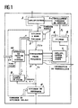
- the fractional division frequency synthesizer which is represented in FIG. 1 comprises a voltage-controlled oscillator 1 coupled by its output to a variable-rank loop divider circuit 2 through separator amplifiers 3. It also includes a divider of reference frequency 4, a phase-frequency comparator 5, a servo control device 6 composed of an amplifier circuit 7 and a loop filter 8, a phase storage circuit 9 and a management interface circuit 10.
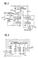
- the variable rank loop divider circuit 2 which is represented in FIG. 2 comprises a predivisor circuit 11 with two modulo Q / Q + 1 and two programmable synchronous counters 12 and 13 coupled to the output of the predivisor circuit 11.
- the predivisor circuit 11 comprises, as shown in FIG. 3, a set of flip-flops mounted in a Johnson ring in which only Q + 1 states are kept to allow the realization of a divider with two modulo Q and Q + 1.
- the number of flip-flops is limited to 4 and flip-flops 14 and 16 form a ring with 8 possible states.
- a two-module 4/5 pre-divider is produced using flip-flops 14, 15 and 16.
- the flip-flop 17 makes it possible to carry out a double extension of the modulos, that is to say, to carry out a division by 8 or by 9.
- the signal to be divided provided by the output of the amplifiers (fig. 1) is applied to the clock inputs CK of flip-flops 14, 15 and 16 through two interface circuits 18 and 19 connected in series.
- the modulo Q or Q + 1 division mode is determined by the logic circuits "or" 20, 21 and 22 placed on the successive loops of the outputs of flip-flops 16, 15 and 14 on the input of flip-flop 14.
- the outputs of the predivisor 11 are selected by circuits "or" 24 and 25 controlled from an MS / SP control bit applied to the input of an inverter circuit 23.
- the output Q1 of the first flip-flop 14 constitutes the output signal of the predivisor and the output of the last flip-flop 17 is inhibited in this case.
- a timing diagram illustrating the operation of the predivisor is represented in FIG. 4. This represents the successive states of the outputs Q1 to Q4 of the flip-flops 14 to 17 as a function of the H states of the frequency signal F S supplied by the oscillator of FIG. 1 through amplifiers 3.
- the two counters 12 and 13 shown in FIG. 2 receive the clock signal H divided by Q or Q + 1 from the predivisor 11. These counters are programmed with the respective values N A and N P and count down simultaneously from these values , at the start of the division cycle by Q + 1, as long as the number N A has not been counted down to zero by the counter 12. When this occurs, the countdown of the counter 12 is stopped and the division rank of the predivisor 11 is positioned on Q by the output of a decoder 26 of the state "O" which controls the inhibition of the counter 12 (input E), and the loading of the division mode of the predivisor 11. At this instant there is (Q + 1) ⁇ N A clock pulses counted. The counting down of the number Np by the counter 13 continues until reaching the state "2" decoded by a decoder 27 formed by a "no or” gate or any equivalent device placed at the output of the counter 13.
- the decoding of state 2 constitutes information at the end of the division cycle. This is synchronized on the rising edge of the output clock of the predivisor 11 and controls the reloading of the counters 12 and 13 via a flip-flop 28, in synchronism with this clock, at the initial values N A and N P.
- the counter 12 is released, the predivisor 11 is positioned to divide by Q + 1 and the cycle begins again.
- the total number of H input clock overruns counted during a division cycle is:
- N (Q + 1) ⁇ N A + (N p - N A )
- the reference divider 4 makes it possible to obtain a reference frequency F R of the loop, submultiple of the external reference frequency. Its division rank is programmed by a 5-bit control word R ⁇ to R4.
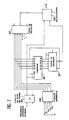
- the divider of the reference frequency is constituted as shown in Figure 7 by a programmable 5-bit binary counter 30 which provides all the division ranges between 2 and 32 inclusive. This circuit counts down from the value programmed on its inputs D to the value "zero", in synchronism with the rising edge of a clock signal supplied by an external reference frequency).
- a decoding gate 31 disposed at the output of the counter 30 detects the state "0” and sends a level “0" on the "LOAD” input of counter 30, which authorizes its reloading at the value programmed on its D inputs.
- the reference frequency which is 12 MHz is obtained after dividing the external reference frequency 24 MHz by 2.
- the TACAN synthesizer loop reference frequency is 1 MHz; it is obtained after division by 24 of this same external reference frequency.
- the phase accumulator circuit 9 which is represented in FIG. 6 comprises a summing circuit 36 (3 bits) followed by a register 37 (4 bits) which makes it possible to synchronize on the rising edge of the clock, at the reference frequency F R , the information obtained at the output of the adder circuit 36 with the overflow signal C OUT of the register 37.
- the outputs (Q1 - Q3) of the register 37 are looped back to the inputs (B O - B2) of the adder circuit 36.
- phase accumulator circuit 9 determines at each reference cycle defined by the period of the signal supplied by the reference frequency divider 5 the mode of division by N or by N + 1 of the variable rank loop divider circuit .
- the module M of the phase accumulator circuit 4 is linked to the reference frequency F R and to the pitch P of the synthesizer by the relation:
- the content of register 37 is increased by the number F at each period 1 / F R of the reference signal.
- the accumulator circuit 37 When the content of register 37 reaches or exceeds the value M, the accumulator circuit 37 provides an overflow signal which is applied to the retaining input cin of the adder circuit 29 to control the incrementation of the division rank N of a unit . (command N, N + 1 in Figures 1 and 2).
- the successive values of the content P k of the accumulator register 37 correspond to the phase difference which exists between the loop signal F S / N and the reference frequency F R.
- the phase-frequency comparator circuit 5 measures the frequency difference between the output signal of the variable rank divider of frequency F S / N and the frequency reference signal F R during the transient loop servo period during d 'a change of frequency.
- the comparator circuit 5 When the loop is stabilized, the comparator circuit 5 provides, at each reference period 1 / F R, a measurement of the phase difference between the signals F S / N and F R.
- This circuit comprises two “D type” flip-flops, 38, 39 coupled to two multiplexer circuits 40, 41.
- the flip-flops 38, 39 are activated on the rising edge of the clock C p , and their Q outputs are looped back to the "Reset" inputs via a "no or” gate 42.
- the transfer characteristic of the comparator circuit 5 must be very linear in this range and without dead zone so as to maintain constant the gain of the phase comparator circuit 5 and therefore the gain of the phase loop.
- the multiplexers 40 and 41 with 2 inputs make it possible to swap the signals at the input of the comparator according to the control signal CPF. This device makes it possible to reverse the direction of control of oscillator 1.
- phase frequency comparator circuit 5 is usefully supplemented by a loop locking detection device shown in FIG. 10 where the elements of the comparator circuit 5 homologous to those of FIG. 8 are represented with the same references.
- This device provides reliable information to detect any malfunction of the synthesizer. For this it uses the signals "UP” and “DOWN” appearing at the output of the comparator circuit 5 and delivers a logic state “1" when the phase loop is locked, or a state "0" otherwise.
- phase-frequency comparator circuit 5 Depending on the situation of the phase loop, various signals may appear at the output of the phase-frequency comparator circuit 5. These different cases are summarized in the table in FIG. 11.
- the signals "UP” and “DOWN” at the output of the comparator circuit 5 are sent to the input of a "or exclusive” circuit 43. They are formed when the loop is not locked, either of a level “1” is a succession of "0" and “1” with a high proportion of "1".
- the output signal from the "OR” circuit 44 is applied to the reset input MR of a counter 45 which has the reference frequency FR as a clock.
- MR 1
- the outputs Q of the counter 45 which are combined at the input of a "NO OR” gate 46 deliver a state " 1 ".
- the counter 45 is reset frequently and has a permanent state "1" at the output of the "NO OR” circuit 46, since it does not have in this case time to finish counting. This state is reversed by the amplifier 47 before being transmitted to the output of the detection device.
- a filter 48 disposed at the output of the "or exclusive" circuit 43 makes it possible to smooth the parasitic pulses which may appear during the transitions of the equilibrium pulses.
- This filter consists of a capacitor CL.
- the loop reacts very quickly and the equilibrium pulses at the output of the phase comparator 5 are not sufficiently disturbed to be detected by this device; the "OR" circuit 44 applies to the input MR of the counter 45 a signal CHF2, coming from the data management interface 10.
- the CHF2 signal to trigger the counting and to indicate the unlocking of the loop during the control phase.
- the servo control device shown respectively for the TDMA and TACAN applications in FIGS. 13A and 13B, comprises a charge-pump amplifier 7, coupled to loop filters 48 and rejectors 49 and to a low-pass filter 50 connected serial.
- the charge-pump amplifier 7 consists of two switched current sources I UP and I DOWN , formed by transistors 50 to 57 which charge and discharge an integration capacitor 62.
- the two current sources comprise two symmetrical UP and DOWN channels each composed of a first differential pair of transistors 50, 51 respectively 52, 53 which performs a level translation to control a second pair 54, 55 respectively 56, 57 of transistors which performs the switching of the charge and / or discharge current of the integration capacity 62.
- the switching command is provided by the output signals "UP" and "DOWN” and their complement supplied by the comparator 5.
- the speed of the switches, each of which is constituted by a differential transistor stage allows to take into account the fine pulses at the output of the phase comparator 5.
- the conversion gain of the phase comparator and charge-pump amplifier 7 assembly is defined by the value of the output current which is optimized as a function of the loop gain and the desired response speed.
- the loop filter 48 formed by the resistor 60 and the capacitors 61 and 62 is determined so as to obtain the characteristics of phase noise and of acquisition time sought.
- a slow TACAN type synthesizer must be able to have a narrow loop bandwidth (cutoff frequency 30 KHz), and a fast TDMA type synthesizer must have a wide loop bandwidth (cutoff frequency 400 KHz).
- rejection filters 49 for the TACAN and 66 for the TDMA formed by series resonant elements centered, for example, on the frequency 12 MHz for the production of the TDMA and 1 MHz synthesizers for the production of TACAN synthesizers.
- the other harmonic lines of the reference frequency are filtered by the loop.
- the fractionation lines at multiple frequencies of 3 MHz are eliminated by means of filter filters 63, 64, 65 centered on the frequencies of 3 MHz, 6 MHz and 9 MHz.
- the other harmonic lines of 3 MH and of frequency higher than 12 MHz do not require specific filtering because they are already strongly attenuated by the loop filtering.
- the lines at 3 and 6 MHz which are closest to the loop bandwidth each require to be reduced to a level below -70 dB c two self L and capacitance rejectors (a 63 bis LC series plug circuit followed by '' a parallel LC circuit to attenuate the lines at 3 MHz and two parallel circuits 64, 64 bis to attenuate the lines at 6 MHz).
- the data management interface which is shown in FIG. 12 manages the synthesizer control information supplied by the radio bus CR of FIG. 1, for the specific operating modes of the TDMA and TACAN synthesizers.
- the control information of the TDMA synthesizer is composed of an 8-bit parallel word, 6 of which are used to define the number of the frequency channel (between 0 and 50) on which the synthesizer must operate.
- the information is taken into account on the rising edge of the pulse of the signal CHF1 which constitutes the clock of a register 67 validated by the low level of the signal ENABLE.
- the channel information CR is applied to an interface circuit 72 and is transformed into control information for the variable rank divider 2 (words N A on 3 bits and N p on 8 bits in this example for programming the counters 12 and 13 FIG. 2) and of the phase accumulator circuit 9 (word F over 3 bits) via a coding circuit 68 connected to the register 67.
- control information for a TACAN synthesizer is constituted in this example by two serial words of 8 parallel bits whose format is shown in FIGS. 15A and 15B.
- bits D0 to D4 forming the 2nd word can all have the value 0.
- the first 8-bit word is taken into account on the rising edge of the first pulse of the CHF1 signal by register 67 under the control of a gate 73.
- the second 8-bit word is taken into account on the rising edge of the second pulse of the CHF1 signal by a register 69 under the control of a door 74.
- a REGISTER SELECT signal combined with the ENABLE signal makes it possible to validate successively the registers 67 and 69.
- a buffer register 70 is validated at the same time as the register 69 in order to transfer to a 16-bit input of a multiplexer 71, the first 8-bit word simultaneously with the second word, on the rising edge of the second pulse of the CHF1 signal.
- the multiplexer 71 receives on its second 16-bit input, the TDMA information at the output of the coding circuit 68.
- This has the advantage of making it possible to select, from a wired TDMA / TACAN command, the control information synthesizer for TDMA mode or TACAN mode.
- the interface circuit also includes a 75 bis sequencer, which delivers a CHF2 signal to select the second pulse of the CHF1 signal in TACAN mode.
- the data management interface can operate, for example, with a clock frequency of 5 MHz.
- oscillator 1 For the TDMA application, oscillator 1 must be able to cover the 1242-1479 MHz frequency band while maintaining a very linear voltage-frequency transfer characteristic to maintain a constant loop gain and spectral purity performance of the synthesizer throughout the frequency range.
- the oscillator For a TACAN synthesizer, the oscillator must be able to cover the transmit and receive frequency bands from 1025 to 1474 MHz.
- the frequency range covered by this oscillator is therefore greater than that covered by the oscillator of the TDMA application, but in this case it is not necessary to have such a high linearity because the preservation of the purity performances spectral in the frequency range is less critical. It is thus possible to obtain, whatever the applications, a floor noise lower than -150 dBc / Hz from a frequency deviation of ⁇ 10% of the central frequency and an output level of the oscillator of +13 dBm.
Landscapes
- Stabilization Of Oscillater, Synchronisation, Frequency Synthesizers (AREA)
Applications Claiming Priority (2)
| Application Number | Priority Date | Filing Date | Title |
|---|---|---|---|
| FR8917080A FR2656480B1 (fr) | 1989-12-22 | 1989-12-22 | Synthetiseur hyperfrequence a division fractionnaire. |
| FR8917080 | 1989-12-22 |
Publications (2)
| Publication Number | Publication Date |
|---|---|
| EP0434527A1 true EP0434527A1 (de) | 1991-06-26 |
| EP0434527B1 EP0434527B1 (de) | 1993-07-14 |
Family
ID=9388884
Family Applications (1)
| Application Number | Title | Priority Date | Filing Date |
|---|---|---|---|
| EP90403602A Expired - Lifetime EP0434527B1 (de) | 1989-12-22 | 1990-12-14 | Mikrowellen-Synthesierer mit einem Teiler mit gebrochenem Teilverhältnis |
Country Status (5)
| Country | Link |
|---|---|
| US (1) | US5122762A (de) |
| EP (1) | EP0434527B1 (de) |
| CA (1) | CA2032419A1 (de) |
| DE (1) | DE69002224T2 (de) |
| FR (1) | FR2656480B1 (de) |
Cited By (3)
| Publication number | Priority date | Publication date | Assignee | Title |
|---|---|---|---|---|
| EP0717502A1 (de) * | 1994-12-16 | 1996-06-19 | Thomson-Csf | Frequenzsynthetisierer für einen VHF-UHF Breitbandempfänger |
| EP0727877A3 (de) * | 1995-02-14 | 1997-02-12 | Matsushita Electric Industrial Co Ltd | Synthetisierer mit schneller Frequenzumschaltung |
| CN1084088C (zh) * | 1996-06-11 | 2002-05-01 | 松下电器产业株式会社 | 频率合成器 |
Families Citing this family (7)
| Publication number | Priority date | Publication date | Assignee | Title |
|---|---|---|---|---|
| US5495505A (en) * | 1990-12-20 | 1996-02-27 | Motorola, Inc. | Increased frequency resolution in a synthesizer |
| US5684795A (en) * | 1996-01-30 | 1997-11-04 | Motorola, Inc. | Method and apparatus for controlling a fractional-N synthesizer in a time division multiple access system |
| US5771182A (en) * | 1996-05-31 | 1998-06-23 | Motorola, Inc. | Bit-serial digital compressor |
| FR2763196B1 (fr) * | 1997-05-07 | 1999-07-30 | Thomson Csf | Synthetiseur de frequence coherent a boucle de phase et pas fractionnaires |
| US5870002A (en) * | 1997-06-23 | 1999-02-09 | Exar Corporation | Phase-frequency lock detector |
| RU2191468C2 (ru) * | 2000-06-21 | 2002-10-20 | Ивановский государственный энергетический университет | Устройство фазовой автоподстройки частоты |
| RU2214043C2 (ru) * | 2001-03-11 | 2003-10-10 | Государственное унитарное предприятие Омский научно-исследовательский институт приборостроения | Синтезатор частот |
Citations (3)
| Publication number | Priority date | Publication date | Assignee | Title |
|---|---|---|---|---|
| US4034309A (en) * | 1975-12-23 | 1977-07-05 | International Business Machines Corporation | Apparatus and method for phase synchronization |
| GB2021338A (en) * | 1978-05-17 | 1979-11-28 | Philips Nv | Frequency synthesizer |
| EP0147307A2 (de) * | 1983-12-27 | 1985-07-03 | Thomson-Csf | Frequenzsynthesierer mit gebrochenem Teilungsverhältnis und mit schwachem Phasenrauschen und Anwendung dieser Synthesierer |
Family Cites Families (1)
| Publication number | Priority date | Publication date | Assignee | Title |
|---|---|---|---|---|
| US4965531A (en) * | 1989-11-22 | 1990-10-23 | Carleton University | Frequency synthesizers having dividing ratio controlled by sigma-delta modulator |
-
1989
- 1989-12-22 FR FR8917080A patent/FR2656480B1/fr not_active Expired - Fee Related
-
1990
- 1990-12-14 DE DE90403602T patent/DE69002224T2/de not_active Expired - Fee Related
- 1990-12-14 EP EP90403602A patent/EP0434527B1/de not_active Expired - Lifetime
- 1990-12-17 CA CA002032419A patent/CA2032419A1/fr not_active Abandoned
- 1990-12-20 US US07/630,890 patent/US5122762A/en not_active Expired - Fee Related
Patent Citations (3)
| Publication number | Priority date | Publication date | Assignee | Title |
|---|---|---|---|---|
| US4034309A (en) * | 1975-12-23 | 1977-07-05 | International Business Machines Corporation | Apparatus and method for phase synchronization |
| GB2021338A (en) * | 1978-05-17 | 1979-11-28 | Philips Nv | Frequency synthesizer |
| EP0147307A2 (de) * | 1983-12-27 | 1985-07-03 | Thomson-Csf | Frequenzsynthesierer mit gebrochenem Teilungsverhältnis und mit schwachem Phasenrauschen und Anwendung dieser Synthesierer |
Cited By (6)
| Publication number | Priority date | Publication date | Assignee | Title |
|---|---|---|---|---|
| EP0717502A1 (de) * | 1994-12-16 | 1996-06-19 | Thomson-Csf | Frequenzsynthetisierer für einen VHF-UHF Breitbandempfänger |
| FR2728410A1 (fr) * | 1994-12-16 | 1996-06-21 | Thomson Csf | Dispositif de synthese de frequence pour recepteur v/uhf large bande |
| US5752175A (en) * | 1994-12-16 | 1998-05-12 | Thomson-Csf | Frequency synthesizer for V/UHF wideband receiver |
| EP0727877A3 (de) * | 1995-02-14 | 1997-02-12 | Matsushita Electric Industrial Co Ltd | Synthetisierer mit schneller Frequenzumschaltung |
| US5694089A (en) * | 1995-02-14 | 1997-12-02 | Matsushita Electric Industrial Co, Ltd. | Fast frequency switching synthesizer |
| CN1084088C (zh) * | 1996-06-11 | 2002-05-01 | 松下电器产业株式会社 | 频率合成器 |
Also Published As
| Publication number | Publication date |
|---|---|
| FR2656480B1 (fr) | 1994-04-15 |
| CA2032419A1 (fr) | 1991-06-23 |
| DE69002224T2 (de) | 1993-10-28 |
| FR2656480A1 (fr) | 1991-06-28 |
| US5122762A (en) | 1992-06-16 |
| EP0434527B1 (de) | 1993-07-14 |
| DE69002224D1 (de) | 1993-08-19 |
Similar Documents
| Publication | Publication Date | Title |
|---|---|---|
| US8395428B2 (en) | Reference clock sampling digital PLL | |
| FR2554994A1 (fr) | Dispositif de generation d'une frequence fractionnaire d'une frequence de reference | |
| US8618967B2 (en) | Systems, circuits, and methods for a sigma-delta based time to digital converter | |
| EP1049285B1 (de) | Frequenzregelkreis | |
| FR2498032A1 (fr) | Synchroniseur de bits pour signaux numeriques | |
| EP0434527B1 (de) | Mikrowellen-Synthesierer mit einem Teiler mit gebrochenem Teilverhältnis | |
| EP0147307B1 (de) | Frequenzsynthesierer mit gebrochenem Teilungsverhältnis und mit schwachem Phasenrauschen und Anwendung dieser Synthesierer | |
| WO2003032495A1 (fr) | Circuit compteur diviseur double mode a phase commutee pour un synthetiseur de frequence | |
| EP1193877A1 (de) | Frequenzsynthesizer mit gebrochenem Teilverhältnis und schneller Abstimmung und entsprechendes Verfahren zur Frequenzsynthese | |
| EP0753941A1 (de) | Frequenzsynthetisierer | |
| EP1193879A1 (de) | Rauscharmer und schnellansprechender Frequenzsynthesierer, und übereinstimmendes Verfahren zur Frequenzsynthese | |
| EP0302562B1 (de) | Frequenz-Synthetisierer mit einer Abstimm-Anzeigeeinrichtung | |
| EP1916768A1 (de) | Vorrichtung und Verfahren zur Erzeugung eines Signals mit beim Start vordefiniertem Transienten | |
| EP3048730B1 (de) | Vorrichtung zur erzeugung einer rückkopplungsschleifenfrequenz | |
| BE1010980A3 (fr) | Synthetiseur de frequence a boucle de verrouillage de phase a division fractionnaire multiple. | |
| CN110581708A (zh) | 锁频环型全数字频率综合器 | |
| EP0550360A1 (de) | Verriegelungsdetektor für eine Phasenregelschleife | |
| EP3764546B1 (de) | Vorrichtung zur frequenzsynthese mit rückkopplungsschleife | |
| EP1411638B1 (de) | Verfahren und Vorrichtung zur Erzeugung eines Signals mit einer dem Produkt einer Referenzfrequenz mit einer reellen Zahl entsprechenden Frequenz | |
| FR2884372A1 (fr) | Boucle a asservissement de phase | |
| EP0645892B1 (de) | Frequenzregelkreis | |
| EP2543147B1 (de) | Vorrichtung für rückkopplungsschleifen-frequenzsysnthese | |
| WO2002001721A1 (fr) | Procede et dispositif de synthese de frequence au moyen d'une boucle a phase asservie | |
| EP1193876A1 (de) | Frequenzsynthesizer und Verfahren zur Frequenzsynthese mit geringem Rauschen | |
| CN116566385A (zh) | 一种频率校准锁相环和频率校准方法 |
Legal Events
| Date | Code | Title | Description |
|---|---|---|---|
| PUAI | Public reference made under article 153(3) epc to a published international application that has entered the european phase |
Free format text: ORIGINAL CODE: 0009012 |
|
| AK | Designated contracting states |
Kind code of ref document: A1 Designated state(s): DE GB IT |
|
| 17P | Request for examination filed |
Effective date: 19911130 |
|
| 17Q | First examination report despatched |
Effective date: 19920130 |
|
| GRAA | (expected) grant |
Free format text: ORIGINAL CODE: 0009210 |
|
| AK | Designated contracting states |
Kind code of ref document: B1 Designated state(s): DE GB IT |
|
| ITF | It: translation for a ep patent filed | ||
| REF | Corresponds to: |
Ref document number: 69002224 Country of ref document: DE Date of ref document: 19930819 |
|
| GBT | Gb: translation of ep patent filed (gb section 77(6)(a)/1977) |
Effective date: 19930826 |
|
| RAP2 | Party data changed (patent owner data changed or rights of a patent transferred) |
Owner name: THOMSON-CSF |
|
| PLBE | No opposition filed within time limit |
Free format text: ORIGINAL CODE: 0009261 |
|
| STAA | Information on the status of an ep patent application or granted ep patent |
Free format text: STATUS: NO OPPOSITION FILED WITHIN TIME LIMIT |
|
| 26N | No opposition filed | ||
| PG25 | Lapsed in a contracting state [announced via postgrant information from national office to epo] |
Ref country code: DE Effective date: 19940901 |
|
| PG25 | Lapsed in a contracting state [announced via postgrant information from national office to epo] |
Ref country code: GB Effective date: 19941214 |
|
| GBPC | Gb: european patent ceased through non-payment of renewal fee |
Effective date: 19941214 |
|
| PG25 | Lapsed in a contracting state [announced via postgrant information from national office to epo] |
Ref country code: IT Free format text: LAPSE BECAUSE OF NON-PAYMENT OF DUE FEES;WARNING: LAPSES OF ITALIAN PATENTS WITH EFFECTIVE DATE BEFORE 2007 MAY HAVE OCCURRED AT ANY TIME BEFORE 2007. THE CORRECT EFFECTIVE DATE MAY BE DIFFERENT FROM THE ONE RECORDED. Effective date: 20051214 |