EP0434950A2 - Simulation d'une impédance complexe et interface pour cette simulation - Google Patents
Simulation d'une impédance complexe et interface pour cette simulation Download PDFInfo
- Publication number
- EP0434950A2 EP0434950A2 EP19900121571 EP90121571A EP0434950A2 EP 0434950 A2 EP0434950 A2 EP 0434950A2 EP 19900121571 EP19900121571 EP 19900121571 EP 90121571 A EP90121571 A EP 90121571A EP 0434950 A2 EP0434950 A2 EP 0434950A2
- Authority
- EP
- European Patent Office
- Prior art keywords
- output
- amplifier
- resistor
- branch
- impedance
- Prior art date
- Legal status (The legal status is an assumption and is not a legal conclusion. Google has not performed a legal analysis and makes no representation as to the accuracy of the status listed.)
- Withdrawn
Links
Images

Classifications
-
- H—ELECTRICITY
- H04—ELECTRIC COMMUNICATION TECHNIQUE
- H04B—TRANSMISSION
- H04B1/00—Details of transmission systems, not covered by a single one of groups H04B3/00 - H04B13/00; Details of transmission systems not characterised by the medium used for transmission
- H04B1/38—Transceivers, i.e. devices in which transmitter and receiver form a structural unit and in which at least one part is used for functions of transmitting and receiving
- H04B1/40—Circuits
- H04B1/54—Circuits using the same frequency for two directions of communication
- H04B1/58—Hybrid arrangements, i.e. arrangements for transition from single-path two-direction transmission to single-direction transmission on each of two paths or vice versa
-
- H—ELECTRICITY
- H04—ELECTRIC COMMUNICATION TECHNIQUE
- H04M—TELEPHONIC COMMUNICATION
- H04M1/00—Substation equipment, e.g. for use by subscribers
- H04M1/58—Anti-side-tone circuits
- H04M1/585—Anti-side-tone circuits implemented without inductive element
Definitions
- the invention relates to a simulation of a complex impedance, in particular the simulation of the impedance of a telephone subscriber line, and a two-wire-four-wire interface with such a simulation.
- Two-wire four-wire interfaces or hybrid circuits have long been known in the telephone and transmission technology.
- Fork circuits are three gates with the task of decoupling a receiver (e.g. the earphone of a telephone set) from a transmitter (e.g. the speech capsule of a telephone unit) and yet coupling both with a two-wire line. To achieve this, a line simulation is also required.
- Cf. for this e.g. K. Steinbuch, W. Rupprecht, communications engineering, Springer-Verlag Berlin and others 1973, pp. 235-241.
- the invention has for its object to provide realizable replicas and two-wire four-wire interfaces with little effort.
- the idea on which the invention is based is to couple the output of an amplifier back to the input of the amplifier via a measuring resistor and a complex feedback network in such a way that the phase relationship between voltage and current required for the simulation occurs at the end of the measuring resistor remote from the amplifier.
- the output amplifier can be designed in such a way that an amplifier results Gain factor is a real multiple of the complex partial impedance, and that the voltage to be amplified by this amplifier is equal to the output voltage of the measuring arrangement, which measures the current in the output resistor designed as an ohmic measuring resistor (claim 2).
- the gain factor of a feedback amplifier is to be proportional to the predetermined partial impedance, this can be achieved in that the partial impedance itself is placed in its feedback branch. Since the amplification factor is further determined by an ohmic resistance, instead of the partial impedance itself, an impedance with the same structure but reduced or enlarged values by the same real factor can be used in all components (claim 3).
- the second stage can be constructed as a summing amplifier. At this point, a signal can then be coupled in without the frequency response being influenced and having to be compensated for by a similar impedance. Nevertheless, the impedance can be constructed as specified and can be reduced or increased by any real factor (claim 4).
- the replica can be made symmetrical by an additional inverter and a further resistor (claim 5).
- the replica should have an ohmic series component, which can be freely specified independently of the impedance to be simulated, as the measuring resistor, which is the measurement of the current on the line can serve, this can be achieved by a purely real acting branch from the output of the measuring arrangement to the input of the output amplifier (claim 7).
- the interface according to the invention advantageously makes use of the replica according to the invention.
- the output amplifier if appropriate together with a further amplifier stage, can also be designed such that results in an amplifier, the gain factor of which is equal to a real multiple of the complex partial impedance, and that the voltage to be amplified by this amplifier is equal to the output voltage of the measuring arrangement, which measures the current in the output resistor in the form of an ohmic measuring resistor (claim 11).
- the input of the received signal is then particularly simple and, without affecting the frequency response, by a two-stage amplifier with the second stage as a summing amplifier.
- the replica is made symmetrical, there is the possibility of simply adding additional information, e.g. Control signals from the connected subscriber are to be transmitted and evaluated by a receiver which responds to unbalanced signals. It is even possible to terminate the two-wire line differently for the earth-symmetrical signals (voice signals) than for the common-mode signals (control signals).
- the earth-symmetrical signals are completed by the simulation, the common-mode signals are completed by the measuring resistors, which are at the output of the amplifier and the inverter in terms of DC voltage to ground (claim 14).
- the outputs of the amplifier and the inverter can be set to a threshold voltage in terms of DC voltage, as a result of which common-mode interference signals become ineffective (claim 15).
- the replica contained in the interface should have an ohmic series component, which can be predefined independently of the impedance to be simulated, and which can serve to measure the current on the line, this can be achieved by a purely real-acting branch from the output of the measuring arrangement to the input of the output amplifier be (claim 16).
- the coupling of the signal from the receiving line advantageously takes place in such a way that the first branch of the interface on the measuring arrangement is coupled into the replica and thus contains the second complex impedance and the purely real-acting branch and that a second purely real acting branch directly from the Receiving line leads to the output amplifier and cancels the effect of the (first) purely real acting branch on the first branch of the interface (claim 17).
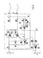
- 1 contains a measuring arrangement M and an amplifier V.
- the measuring arrangement M consists of a measuring resistor RM and a measuring amplifier.
- the amplification factor is chosen equal to 1.
- the measuring resistor RM connects the output of the amplifier V to a connection a, the replica N. The other connection is grounded.
- the measuring resistor RM is flowed through by the current i flowing through the simulation N.
- the voltage u lies between the connections of the replica N.
- the voltage u is also at the output of the measuring arrangement.
- the amplifier V is constructed in two stages with a first amplifier stage VS1 and a second amplifier stage VS2, each with an operational amplifier.
- the inverting input of the operational amplifier of the first amplifier stage is connected to its output via a feedback resistor RS and to the output of the measuring arrangement through a complex impedance Z.
- the inverting input of the operational amplifier of the second amplifier stage is connected to its output via a feedback resistor R4, to the output of the first amplifier stage via a resistor R2 and to the output of the measuring arrangement M via a resistor R3.
- a different impedance Z can be used to simulate the impedance Zin.
- a capacitance of e.g. 115 nF instead of a capacitance of e.g. 115 nF a smaller capacitance with a standardized size, e.g. 1 nF can be used. Such capacities are also easier to maintain with tighter tolerance. Both the mechanical size and the price can be reduced to around 1/10.
- the simulated impedance has an ohmic series component which is at least as large as the measuring resistor RM.
- the measuring resistor can be chosen to be of any size.
- Fig. 2 now shows an inventive Two-wire four-wire interface with a replica N according to the invention contained therein.
- This interface circuit is used to connect a unidirectionally operated receiving line E and a unidirectionally operated transmission line S on the one hand to a bidirectionally operated two-wire line a, b.
- the two-wire line a, b is completed with the replica N.
- the replica N is constructed here in earth symmetry. This is achieved by the inverter I and the division of the measuring resistor into the measuring resistors RS1 and RS2.
- the measuring arrangement M is constructed as a differential amplifier.
- the branch from the reception line E to the two-wire line a, b is coupled into the measuring arrangement M in the example according to FIG. 2 via a resistor R9. It thus leads primarily via the complex impedance Z to the amplifier stage VS2 and from there via the inverter I and the measuring resistors RS1 and RS2 to the two-wire line a, b.
- the effect of this signal routing is the same as that of the circuit protected by European Patent 0 171 692. To understand this, reference is made to the associated patent specification. In the present case, however, the purely real-acting branch has a disturbing effect via resistor R3.
- the interface has a transmission amplifier SV which on the one hand evaluates the output voltage of the measuring arrangement M and on the other hand adds a signal proportional to the voltage on the receiving line E via a resistor R10 in order to compensate for its share in the output voltage of the measuring arrangement M.
- the transmitter amplifier SV would also have to take over the measurement of the voltage on the two-wire line.
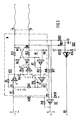
- the interface circuit shown in FIG. 3 serves to connect a unidirectionally operated reception line E and a unidirectionally operated transmission line S on the one hand to a bidirectionally operated two-wire line a, b.
- the two-wire line a, b is completed with a replica N.
- the signal coming from the receiving line E is fed into the replica via a summing amplifier, amplifier stage two, VS2, contained in the replica N, and thus reaches the two-wire line a, b.
- the interface has a transmission amplifier SV, which on the one hand evaluates the voltage on the two-wire line a, b in a differential amplifier circuit and on the other hand adds a signal that is proportional to the voltage on the receiving line E in correct phase in order to determine the proportion of the voltage in the two-wire line a, b balance that comes from the receiving line E.
- control signal receiver SSE which taps the center potential on the two-wire line a, b and compares it with a predetermined threshold value in a Schmitt trigger circuit, in order to derive a digital signal DS from a common-mode signal present on the two-wire line a, b.
- an analog signal could also be transmitted as a common mode signal.
- the prerequisite for this would be negligible common-mode interference signals and a design of the control signal receiver SSE in an amplifier circuit and not in a Schmitt trigger circuit. In any case, it must be taken into account that the two-wire line a, b is not terminated correctly for common-mode signals, but is actually terminated.
- the interface is usually part of a subscriber line circuit.
- the other functions are not shown here.
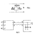
- the impedance to be simulated is shown in FIG. 4. It consists of the series connection of an ohmic resistor Rv with a complex partial impedance Zp, which here consists of the parallel connection of an ohmic resistor Rp and a capacitance Cp.
- This impedance is now realized by the simulation N according to FIG. 3.
- the embodiment shown is earth-symmetrical and has the possibility of feeding the signal from the reception line without the need for frequency response compensation.
- Another type of feeding this signal is that of feeding current, for example together with the remote feed current, directly into the two-wire line a, b.
- An example of a current feed is shown in DE-OS 34 28 106 (1 in Fig. 3).
- the replica N according to FIG. 3 contains a measuring arrangement M, a two-stage amplifier with an amplifier stage one, VS1, and the already mentioned amplifier stage two, VS2, and an inverter I.
- The, here two-stage, amplifier now amplifies the output signal of the measuring arrangement M in such a way that its output voltage to the output current behaves like the complex partial impedance. Its gain factor must therefore be equal to a real multiple of this partial impedance.
- the gain factor of a feedback operational amplifier is proportional to its feedback resistance (R4 in case VS2) and inversely proportional to its series resistor (R2 in the case of VS2).
- An amplifier in the feedback branch of which the predetermined partial impedance Zp lies and whose series resistor is real, therefore has the required amplification factor.
- a similar impedance the components of which are in the same relationship to one another as with the partial impedance Zp, has the same effect if the series resistor is also changed accordingly. Even a gain stage with a real gain factor, such as the second amplifier stage, VS2, does not change the basic behavior.
- the division of the amplifier into two with a real amplifying second stage has the advantage that another signal, here the signal from the receiving line E, can be added without any problems. If this is not necessary, for example if this signal is fed directly into the two-wire line as mentioned above, a single-stage amplifier is sufficient.
- a single-stage amplifier can also be used as a summing amplifier. Then either the series resistor with which the signal is added from the input line must have the same complex structure as the feedback resistor, or the series resistor (here R2) with which the signal of the measuring arrangement M is added must be designed in such a way be that its complex resistance is inversely proportional to the partial impedance Zp.
- the circuit becomes symmetrical with respect to earth. Both can be omitted if symmetry is not required.
- both wires of the two-wire line a, b can be raised or lowered with respect to earth by in each case a DC voltage via an additional one at the corresponding inputs of the second amplifier stage VS2 and the inverter I. Series resistor is added. This is shown in dashed lines in FIG. 3.
- FIG. 5 A preferred application is shown in FIG. 5.
- the interface with the replica contained therein is shown very schematically, and on the right, connected to it via the two-wire line, a telephone device.
- the telephone terminal is shown only to the extent that the generation of the control signal, digital signal DS, is affected.
- Both wires a and b of the two-wire line are each connected to earth via a controlled current source.
- the current source is controlled by the digital signal DS.
Landscapes
- Engineering & Computer Science (AREA)
- Signal Processing (AREA)
- Computer Networks & Wireless Communication (AREA)
- Interface Circuits In Exchanges (AREA)
Applications Claiming Priority (4)
| Application Number | Priority Date | Filing Date | Title |
|---|---|---|---|
| DE3942758 | 1989-12-23 | ||
| DE19893942758 DE3942758A1 (de) | 1989-12-23 | 1989-12-23 | Nachbildung einer komplexen impedanz und schnittstelle mit einer solchen nachbildung |
| DE19904013885 DE4013885A1 (de) | 1990-04-30 | 1990-04-30 | Nachbildung einer komplexen impedanz und schnittstelle mit einer solchen nachbildung |
| DE4013885 | 1990-04-30 |
Publications (2)
| Publication Number | Publication Date |
|---|---|
| EP0434950A2 true EP0434950A2 (fr) | 1991-07-03 |
| EP0434950A3 EP0434950A3 (en) | 1992-07-22 |
Family
ID=25888429
Family Applications (1)
| Application Number | Title | Priority Date | Filing Date |
|---|---|---|---|
| EP19900121571 Withdrawn EP0434950A3 (en) | 1989-12-23 | 1990-11-10 | Simulation of a complex impedance and interface for same |
Country Status (1)
| Country | Link |
|---|---|
| EP (1) | EP0434950A3 (fr) |
Cited By (2)
| Publication number | Priority date | Publication date | Assignee | Title |
|---|---|---|---|---|
| EP0579891A1 (fr) * | 1992-07-22 | 1994-01-26 | STMicroelectronics S.r.l. | Circuit pour la réalisation d'une impédance associée à un circuit de parole d'un poste téléphonique |
| CN114844498A (zh) * | 2022-04-21 | 2022-08-02 | 无锡锐科光纤激光技术有限责任公司 | 防信号干扰转接卡 |
Family Cites Families (3)
| Publication number | Priority date | Publication date | Assignee | Title |
|---|---|---|---|---|
| GB2087199A (en) * | 1980-10-16 | 1982-05-19 | Texas Instruments Ltd | Amplifiers for driving balanced lines |
| CA1182230A (fr) * | 1982-12-17 | 1985-02-05 | Patrick R. Beirne | Circuit d'interface pour ligne d'abonne |
| JP2645022B2 (ja) * | 1987-08-21 | 1997-08-25 | 株式会社東芝 | 加入者回路 |
-
1990
- 1990-11-10 EP EP19900121571 patent/EP0434950A3/de not_active Withdrawn
Cited By (4)
| Publication number | Priority date | Publication date | Assignee | Title |
|---|---|---|---|---|
| EP0579891A1 (fr) * | 1992-07-22 | 1994-01-26 | STMicroelectronics S.r.l. | Circuit pour la réalisation d'une impédance associée à un circuit de parole d'un poste téléphonique |
| US5459787A (en) * | 1992-07-22 | 1995-10-17 | Sgs-Thomson Microelectronics S.R.L. | Circuit for the implementation of an impedance for a telephone speech circuit |
| CN114844498A (zh) * | 2022-04-21 | 2022-08-02 | 无锡锐科光纤激光技术有限责任公司 | 防信号干扰转接卡 |
| CN114844498B (zh) * | 2022-04-21 | 2025-12-16 | 无锡锐科光纤激光技术有限责任公司 | 防信号干扰转接卡 |
Also Published As
| Publication number | Publication date |
|---|---|
| EP0434950A3 (en) | 1992-07-22 |
Similar Documents
| Publication | Publication Date | Title |
|---|---|---|
| DE69011147T2 (de) | Elektronische Anschlusseinrichtung für eine Teilnehmerleitung. | |
| DE2413075A1 (de) | Konferenz-brueckenschaltung | |
| DE2834673C2 (de) | Schaltung einer Verbindungsleitung zur Signalübertragung zwischen symmetrischen a- und b-Klemmen und einem unsymmetrischen Leiterpaar | |
| DE2250859C2 (de) | Schaltungsanordnung für den Übergang von Zwei- auf Vierdrahtbetrieb für Fernmelde-, insbesondere Fernsprechvermittlungsanlagen | |
| EP0434950A2 (fr) | Simulation d'une impédance complexe et interface pour cette simulation | |
| EP0436808B1 (fr) | Amplificateur de sommation avec un facteur de pondération complexe et interface avec un tel amplificateur de sommation | |
| EP0037940B1 (fr) | Circuit pour branchement à deux fils d'un abonné téléphonique à une ligne pour des signaux sortants et une ligne pour des signaux entrants | |
| DE3942758A1 (de) | Nachbildung einer komplexen impedanz und schnittstelle mit einer solchen nachbildung | |
| EP0443117B1 (fr) | Connexion analogique de ligne | |
| DE4013885A1 (de) | Nachbildung einer komplexen impedanz und schnittstelle mit einer solchen nachbildung | |
| EP0416679A1 (fr) | Dispositif de transmission de données avec liaison de transmission de données différentielle | |
| EP0209716A2 (fr) | Circuit pour la suppression de signaux perturbateurs sur la ligne de branchement de réception d'un circuit de ligne d'abonné réalisé par des composants électroniques sans l'emploi d'un transformateur pour les signaux de parole | |
| EP0037518B1 (fr) | Circuit hybride sans transformateur | |
| DE3236148A1 (de) | Schaltungsanordnung zum einstellen der verstaerkung eines verstaerkers | |
| EP0467367B1 (fr) | Circuit d'interface de ligne d'abonné pour la connexion d'une ligne d'abonné pour la transmission de signaux analogiques d'abonné à un central téléphonique numérique à multiplexage temporel | |
| EP0139814A2 (fr) | Circuit égalisateur actif | |
| DE3611226C2 (fr) | ||
| EP0477660B1 (fr) | Circuit de reception d'informations transmises sur les lignes de puissance | |
| DE4010001C1 (en) | Amplifier with stepped adjustable gain - provided by three stages switched in cascade and comprising intermediate attenuator between input and output amplifiers | |
| DE3108647A1 (de) | Teilnehmeranschlussschaltung | |
| DE2130082C3 (de) | Schaltungsanordnung zur Übertragung von Gleichstromtelegrafiezeichen und Datensignalen | |
| DE3806045C1 (en) | Electronic bridge circuit | |
| DE1952549C3 (de) | Schaltungsanordnung zur Übertragung von Impulsen | |
| DE900473C (de) | Nachrichtenuebertragungsanlage fuer beide Verkehrsrichtungen mit fremdgesteuerten Schaltern zur abwechselnden OEffnung beider Verkehrswege | |
| AT401839B (de) | Schaltungsanordnung zum komplexen leitungsabschluss einer an eine kommunikationseinrichtung angeschlossene zweidrahtleitung |
Legal Events
| Date | Code | Title | Description |
|---|---|---|---|
| PUAI | Public reference made under article 153(3) epc to a published international application that has entered the european phase |
Free format text: ORIGINAL CODE: 0009012 |
|
| AK | Designated contracting states |
Kind code of ref document: A2 Designated state(s): AT BE CH DE DK ES FR GB GR IT LI LU NL SE |
|
| PUAL | Search report despatched |
Free format text: ORIGINAL CODE: 0009013 |
|
| AK | Designated contracting states |
Kind code of ref document: A3 Designated state(s): AT BE CH DE DK ES FR GB GR IT LI LU NL SE |
|
| RAP3 | Party data changed (applicant data changed or rights of an application transferred) |
Owner name: ALCATEL SEL AKTIENGESELLSCHAFT |
|
| 17P | Request for examination filed |
Effective date: 19921212 |
|
| 17Q | First examination report despatched |
Effective date: 19960311 |
|
| STAA | Information on the status of an ep patent application or granted ep patent |
Free format text: STATUS: THE APPLICATION IS DEEMED TO BE WITHDRAWN |
|
| 18D | Application deemed to be withdrawn |
Effective date: 19980224 |