EP0435390A2 - Gegen Gleichtaktströme unempfindliche Halbbrücken-Treiberstufe - Google Patents
Gegen Gleichtaktströme unempfindliche Halbbrücken-Treiberstufe Download PDFInfo
- Publication number
- EP0435390A2 EP0435390A2 EP90203379A EP90203379A EP0435390A2 EP 0435390 A2 EP0435390 A2 EP 0435390A2 EP 90203379 A EP90203379 A EP 90203379A EP 90203379 A EP90203379 A EP 90203379A EP 0435390 A2 EP0435390 A2 EP 0435390A2
- Authority
- EP
- European Patent Office
- Prior art keywords
- high side
- sense resistors
- bridge
- transistor
- lines
- Prior art date
- Legal status (The legal status is an assumption and is not a legal conclusion. Google has not performed a legal analysis and makes no representation as to the accuracy of the status listed.)
- Granted
Links
Images

Classifications
-
- H—ELECTRICITY
- H02—GENERATION; CONVERSION OR DISTRIBUTION OF ELECTRIC POWER
- H02M—APPARATUS FOR CONVERSION BETWEEN AC AND AC, BETWEEN AC AND DC, OR BETWEEN DC AND DC, AND FOR USE WITH MAINS OR SIMILAR POWER SUPPLY SYSTEMS; CONVERSION OF DC OR AC INPUT POWER INTO SURGE OUTPUT POWER; CONTROL OR REGULATION THEREOF
- H02M7/00—Conversion of AC power input into DC power output; Conversion of DC power input into AC power output
- H02M7/42—Conversion of DC power input into AC power output without possibility of reversal
- H02M7/44—Conversion of DC power input into AC power output without possibility of reversal by static converters
- H02M7/48—Conversion of DC power input into AC power output without possibility of reversal by static converters using discharge tubes with control electrode or semiconductor devices with control electrode
- H02M7/505—Conversion of DC power input into AC power output without possibility of reversal by static converters using discharge tubes with control electrode or semiconductor devices with control electrode using devices of a thyratron or thyristor type requiring extinguishing means
- H02M7/515—Conversion of DC power input into AC power output without possibility of reversal by static converters using discharge tubes with control electrode or semiconductor devices with control electrode using devices of a thyratron or thyristor type requiring extinguishing means using semiconductor devices only
- H02M7/519—Conversion of DC power input into AC power output without possibility of reversal by static converters using discharge tubes with control electrode or semiconductor devices with control electrode using devices of a thyratron or thyristor type requiring extinguishing means using semiconductor devices only in a push-pull configuration
Definitions
- the present invention relates to a device for controllably driving a half-bridge including a high side switch means and a low side switch means, said high side switch means coupled to an output of the half-bridge and having a drive input, said device including a high side driver comprising: a high side drive output for coupling to the drive input of said high side switch means for selectively placing said high side switch means in an ON state or an OFF state; means for receiving high side control currents in two lines.
- High voltage half-bridge circuits employing transistor switch means such as MOSFETs and IGTs find use in a variety of power applications including D.C. to A.C. inverters, motion control devices, switch mode power supplies and lighting ballasts.
- the required D.C. supply can range up to 500 volts with the output of the half bridge capable of undergoing transitions between zero volts and the D.C. supply voltage at high slew rates.
- Monolithically integrated half-bridge driver circuits have recently become available as described, for example, in D.F. Henderson, "An HVIC MOSFET/IGT Driver For Half-bridge Topologies", HFPC, May 1988 Proceedings, pp. 237-245.
- the bridge driver described therein is of the dual channel type, comprising a high side channel including a high side driver, powered by a bootstrap supply voltage, for driving the upper of high side transistor of the half-bridge and a low or ground side channel including a low side driver for driving the low side or lower transistor thereof.
- the high side driver, and its bootstrap supply voltage floats on the output of the half-bridge in order to properly drive the high side transistor.
- a level shifter is included in the high side channel for transmitting control signals over two lines from ground potential to a receiving portion of the high side driver.
- control signals are typically in the form of a downwardly directed "ON” current pulse transmitted on one control line for selectively placing the high side transistor in a conductive state and a downwardly directed “OFF” current pulse transmitted on the other control line for selectively placing the high side transistor in a non-conductive state.
- the state of the high side transistor is controlled by an R/S flip-flop in the high side driver which is set by the "ON” pulse and reset by the "OFF" pulse.
- Half-bridge drivers of the type described are prone to transient currents induced in the control lines due to high positive and negative slew rates (>10 kv/microsecond) at the output of the bridge which, when acting effectively across a parasitic capacitance of a few picofarads, can cause the parasitic capacitance to appear as a source of upwardly or downwardly directed transient currents in the control lines having amplitudes which may be greater than a few tens of milliamperes. Such transient currents tend to be induced simultaneously in both control lines in what we term a "common mode".
- each line has its own sense resistors in series with said each line and differential means are coupled between said sense resistors and said high side drive output for controlling the state of the high side switch means in response to the difference between the voltages at said sense resistors within an operational dynamic range.
- the differential means preferably includes a differential amplifier means having two outputs of opposite polarity providing "SET” and “RESET” inputs to a flip-flop whose logical state controls the conductive state of the driven power switch means.
- a further feature of the invention is the incorporation of dead zone in the center of the operational input dynamic range of the differential receiver means to provide noise immunity.
- Yet another feature of the invention is the provision of matching means in the level shifter transmitter portion which adjusts the amplitudes of the "ON" and "OFF" control current pulses in relation to measures of the dead zone of the differential amplifier means and of the resistance of the sense resistors.
- Other aspects of the invention depend on the choice of value for the sense resistors. If the sense resistors are chosen of relatively low ohmic value so that the voltages developed by the common mode currents across the sense resistors are well within the input dynamic range of the differential means, control is possible during the instants of the common mode currents, whether upwardly or downwardly directed.
- the sense resistors may be chosen at higher ohmic values, for reduced power requirements in the transmitter and/or for use with extremely high slew rates at the output of the half-bridge, but then clamp means are utilized to limit the voltages developed by the common mode currents across the sense resistors with respect to the bootstrap voltage supply base, for the purpose of protecting the differential means from excessive inputs.
- the aforementioned half-bridge driver is implemented in either bipolar and MOS technology suitable for a high voltage integrated circuit and utilizes elements realizable in such technologies.
- HVIC high voltage integrated circuit
- a load 30 diagrammatically shown as the series combination of an inductance L L and resistance R L .
- transistors T H and T G are illustratively enhancement type NMOS which are turned on by a positive gate to source voltage of a predetermined amount.
- IGT transistors may serve as suitable power switch means.
- Half-bridge driver 10 comprises a high side driver 36 having an output voltage between lines 38 and 40 providing the gate to source voltage for the high side transistor T H .
- Line 40 is connected to output mode 18 such that the output voltage between lines 30 and 40 floats on V out .
- a ground side driver 42 is also provided in half-bridge driver 10 to provide the gate to source voltage for transistor T G between lines 44 and 46.
- Line 46 is connected to negative supply rail 26 such that the output voltage between lines 44 and 46 floats on power ground 26.
- Ground side driver 42 also receives an externally applied power source +V A applied between lines 48 and 46 and across capacitor 50.
- High side driver 36 receives an externally supplied bootstrap voltage V B between lines 52 and 40 and across capacitor 54, which is developed from voltage +V A by the charging of capacitor 54 via a diode 55 connected between lines 48 and 52.
- bootstrap voltage V B floats on output voltage V out and when transistor T H is off and transistor T G is on, such that V out is substantially coupled to power ground, capacitor 54 is charged via diode 52 to a voltage approaching +V A .
- Half-bridge driver 10 is controlled by an external system control 56 which provides to a logic interface portion 64 of half-bridge driver 10, a high side transistor control logic signal on line or channel 58 and a ground side transistor control logic signal on line or channel 60 which signals are referred to a common control or logic ground line 62.
- Logic ground 62 is not directly connected to power ground 26 in order to provide immunity to control 56 and logic interface 64 from power switching transients.
- Logic interface 64 provides control signals on lines 66 to level shifter 68 which performs a voltage translation of the control signals to the high side driver 36, which floats on V out , and to the ground side driver 42, which floats on power ground.
- the translation in each case may take the same form involving a transmitter at the output of the level shifter and a receiver at the input of the applicable driver, 36 or 42.
- control is obtained by transmitting a current pulse I on on line 70 for placing high side transistor T H in a conductive state and by transmitting a current pulse I off on line 72 for placing high side transistor T H in a non-conductive state.
- Similar control signals may be provided on lines 74 between level shifter 68 and ground side driver 42 for control of the conductive-state of the ground side transistor T G .
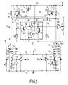
- FIG. 2 illustrates, in its lower part, the transmitter portion 76 of level shifter 68, and, in its upper part the receiver portion 78 of high side driver 36, which portions are connected by lines 70 and 72.
- Transmitter portion 76 which is powered by the logic power supply base V L between lines 80 and logic ground 62, receives pulsatile control input voltage V on and V off for respectively generating downwardly directed current pulses I on in line 70 and I off in line 72. It is intended that the current pulse I on will be transmitted alone to place the high side transistor T H in a conductive state and the current pulse I off will be applied alone to place the high side transistor T H in a non-conductive state.
- the receiver portion 78 is powered by the bootstrap voltage V B , directed between lines 52 and 40, which floats on the output voltage V out of half-bridge 12.
- the upper line 52 has the voltage V D which equals the sum of the instantaneous output voltage V out plus the bootstrap voltage V B .
- Equal sense resistors R1 and R2 are connected from line 52 respectively to control lines 70 and 72 in order to develop control voltages due to the control currents I on and I off .
- the voltages V1 and V2 respectively at the lower ends of the resistors R1 and R2. As should be apparent, a downwardly directed voltage pulse will be caused at V1 due to a current pulse I on in line 70 while a negatively directed voltage pulse will be caused at V2 due to a current pulse I off in line 72.
- the present invention in order to provide insensitivity to voltages due to common mode currents I C incorporates a double differential amplifier means, comprising matched PNP transistors T1 and T2 and matched resistors R5 and R6, for responding to the difference between the voltages V1 and V2.
- the base emitter junctions of the transistors T1 and T2 are connected in opposite directions between V1 and V2.
- base 84 of transistor T1 and emitter 86 of transistor T2 are connected to V1 while base 88 of transistor T2 and emitter 90 of transistor T1 are connected to V2.
- the collectors 92 and 94 of transistors T1 and T2 are respectively connected to the upper ends of resistors R5 and R6 while the lower ends of these resistors are connected to line 40.
- common mode currents I C will produce substantially equal voltages V1 and V2 which will not turn on transistors T1 or T2 while the current pulse I on flowing only in line 70 will turn on at transistor T1 and the current pulse I off flowing only in line 72 will turn on transistor T2.
- the "set” and “reset” outputs V S and V R of the aforementioned dual differential amplifier means are inputted to a R/S flip-flop 96 which is comprised of a pair of inverters I3 and I4 each having its output forming the input of the other in a regenerative loop.
- NPN transistor T5 has its collector at the junction 98 between the input to inverter I3 and the output of inverter I4, its emitter 100 connected to line 40 and its base 102 connected to V S .
- V S will turn on transistor T5 in response to a current pulse I on which will pull junction 98 low and thereby setting the voltage at the junction 104 between the output of inverter I3 and the input of inverter I4 to a high condition.
- Junction 104 forms the output of flip-flop 96 and is input to a buffer 106 having the output 38 for controlling the gate of the high side transistor T H of half-bridge 12.
- NPN transistor T6 is similarly connected with its collector at junction 104, its base 107 connected to V R and its emitter 108 connected to line 40.
- Dual amplifier means comprising transistors T1 and T2 also has an inherent central dead zone such that the difference between voltages V1 and V2 must exceed the V be of the transistors T1 and T2 in order to effect the desired turnon of the transistor T1 or T2.
- This dead zone is desirable for providing a measure of immunity to noise currents in lines 70 and 72 which develop voltages across the sense resistors R1 and R2.
- the current pulses I on or I off must be of sufficient amplitude for the voltages they develop cross resistors R1 and R2 to exceed V be .
- V be is 0.7 volts, and it is therefore desired to generate a voltage of 1 volt across the sense resistors R1 or R2 in response to the current pulses I on or I off , and the resistors are 200 ohms, then the amplitude of the current pulses must be at least 5 ma, which may require significant power to transmit.
- clamp means are advantageously utilized to limit the voltage developed across the sense resistors R1, R2.
- these clamp means comprise transistors T9 through T13.
- NPN transistors T9 and T12 act as upwardly directed diodes across the sense resistors R1 and R2 respectively which prevent the voltages V1 and V2 from rising more than V be above voltage V D .
- the transistor T13 which acts as a diode directed between line 52 and the bases 110 and 112 of NPN transistors T11 and T10 whose emitters 114, 116 are connected respectively to the voltages V1 and V2 and whose collectors 118, 120 are connected to line 52. These clamping means thereby establish a dynamic range for the voltages V1 and V2 within which the differential amplifier means may respond.
- the transmitter portion 76 is preferably matched to the receiver portion 78 to compensate for temperature or manufacturing variations in the resistors R1 and R2 and the transistors T1 and T2.
- the transmitter portion 76 receives as inputs the voltages V on and V off developed by logic interface 64 which are input to inverters I1 and I2 respectively.
- the output of inverter I1 is fed to the junction 119 of the base of NPN transistor T7 and collector of NPN transistor T3.
- the emitter of transistor T7 and base of transistor T3 are joined at 12 to the upper end of resistor R3 while the lower end of resistor R3 and the emitter of transistor T3 are connected to logic ground 62.
- the collector of transistor T7 is connected at 122 to the source of an enhancement type NMOS FET transistor T on .
- NMOS FET T on has its gate 124 connected to V L line 80, its drain 126 connected to control line 70 and its backgate 128 connected to logic ground 62.
- NMOS FET transistor T on acts as a well-defined barrier between the high slew rates present in the receiver 78 and the collector of transistor T7 which sources I on .
- the output of inverter I2 is connected to the junction 130 of the base of NPN transistor T8 and the collector of NPN transistor T4, the emitter of transistor T8 and the base of transistor T4 are connected to the upper end of resistor R4 at junction 132, and the lower end of resistor R4 and the emitter of transistor T4 are connected to logic ground 62.
- the collector of transistor T8 is connected at 134 to the source of NMOS FET transistor T off .
- Transistor T off further has its backgate 136 connected to logic ground 62, its gate 138 connected to V L line 80 and its drain 140 connected to control line 72 to form a barrier similarly to transistor T on .
- transistor T4 is matched to transistors T1 and T2 and resistor R4 is matched to resistors R1 and R2.
- R4 may be chosen somewhat less than R3 to produce a current amplitude I off greater than the current amplitude I on for enhancing the response to an off command.
- the embodiment of Figure 2 is amenable to an integrated circuit realization in which the various bipolar elements and resistors allow for matching the components in temperature characteristics and matching the resistors in resistance value.
- FIG 3 there is illustrated an alternate receiver portion 142 using primarily MOSFET technology, in which similar parts are similarly labeled to Figure 2.
- the gate 144 of PMOS FET T1 and the source 146 of PMOS FET T2 are connected to V1 while the gate 148 of T2 and source 150 of T1 are connected to V2 in a manner analogous to Figure 2 to produce the voltages V S and V R across resistors R5 and R6.
- the clamping means is somewhat different, however, from Figure 2 utilizing MOSFET transistors T9 and T10 with their source, gate and backgate connected respectively to voltages V1 and V2 and their drains connected to voltages V D .
- Transistors T9 and T10 are constructed in a known manner to have a parasitic diode junction directed from V1 and V2 respectively to V D . As a consequence, these transistors prevent V1 and V2 from rising more than V be above V D . Additionally, for forming parasitic diodes parallel to those formed by T9 and T10 to further prevent the voltages V1 and V2 from rising more than V be above V D , the backgates 152 and 154 of transistors T1 and T2 are tied to V D to develop parasitic diodes in each transistor directed from source to backgate.
- the NPN transistors T11 and T12 are provided with their bases 156, 158 connected to V out , their emitters 160, 162 connected respectively to V1 and V2 and their collectors 164, 166 connected to V D . These transistors T11 and T12 prevent V1 and V2 from falling more than V be below V out . It should be equally understood, that if R1 and R2 are sufficiently low in ohmic value that the voltages V1 and V2 never fall close to V out , the various clamping means may not be required.
Landscapes
- Engineering & Computer Science (AREA)
- Power Engineering (AREA)
- Electronic Switches (AREA)
- Dc-Dc Converters (AREA)
- Power Conversion In General (AREA)
- Inverter Devices (AREA)
Applications Claiming Priority (2)
| Application Number | Priority Date | Filing Date | Title |
|---|---|---|---|
| US07/459,095 US4994955A (en) | 1989-12-29 | 1989-12-29 | Half-bridge driver which is insensitive to common mode currents |
| US459095 | 1989-12-29 |
Publications (3)
| Publication Number | Publication Date |
|---|---|
| EP0435390A2 true EP0435390A2 (de) | 1991-07-03 |
| EP0435390A3 EP0435390A3 (en) | 1993-02-24 |
| EP0435390B1 EP0435390B1 (de) | 1995-03-15 |
Family
ID=23823384
Family Applications (1)
| Application Number | Title | Priority Date | Filing Date |
|---|---|---|---|
| EP90203379A Expired - Lifetime EP0435390B1 (de) | 1989-12-29 | 1990-12-18 | Gegen Gleichtaktströme unempfindliche Halbbrücken-Treiberstufe |
Country Status (4)
| Country | Link |
|---|---|
| US (1) | US4994955A (de) |
| EP (1) | EP0435390B1 (de) |
| JP (1) | JP3037760B2 (de) |
| DE (1) | DE69017869T2 (de) |
Cited By (3)
| Publication number | Priority date | Publication date | Assignee | Title |
|---|---|---|---|---|
| FR2717642A1 (fr) * | 1994-03-04 | 1995-09-22 | Int Rectifier Corp | Commande à portes MOS de circuits ballast. |
| WO2003055072A1 (en) * | 2001-12-21 | 2003-07-03 | Bang & Olufsen Icepower A/S | Half-bridge driver and power conversion system with such driver |
| ES2223280A1 (es) * | 2003-07-14 | 2005-02-16 | Electronica De Balastos,S.L. | Sistema de manejo de la parte alta (hsd) de un dispositivo semipuente o puente para un circuito electronico de conmutacion. |
Families Citing this family (30)
| Publication number | Priority date | Publication date | Assignee | Title |
|---|---|---|---|---|
| JP2634306B2 (ja) * | 1990-08-08 | 1997-07-23 | 三菱電機株式会社 | インバータ装置の駆動回路 |
| DE4237843A1 (de) * | 1992-11-10 | 1994-05-11 | Philips Patentverwaltung | Schaltungsanordnung zum Betreiben einer induktiven Last |
| EP0608667B1 (de) * | 1993-01-29 | 1996-08-21 | STMicroelectronics S.r.l. | Treiberschaltung für einen Feldeffekttransistor in einer Halbbrückenausgangsstufe |
| GB9302942D0 (en) * | 1993-02-13 | 1993-03-31 | Attwood Brian E | Low cost,low current power supply |
| US5373435A (en) * | 1993-05-07 | 1994-12-13 | Philips Electronics North America Corporation | High voltage integrated circuit driver for half-bridge circuit employing a bootstrap diode emulator |
| JP2896342B2 (ja) * | 1995-05-04 | 1999-05-31 | インターナショナル・レクチファイヤー・コーポレーション | 半波ブリッジ構成における複数のパワートランジスタを駆動し、かつ出力ノードの過度の負の振動を許容する方法及び回路、並びに上記回路を組み込む集積回路 |
| US5793193A (en) * | 1996-02-15 | 1998-08-11 | Harris Corporation | DC-to-DC converter having enhanced control features and associated methods |
| US5821740A (en) * | 1996-02-15 | 1998-10-13 | Harris Corporation | DC-to-DC converter having fast over-current detection and associated methods |
| US5808883A (en) * | 1996-02-15 | 1998-09-15 | Harris Corporation | DC-to-DC converter having charge pump and associated methods |
| JP3970960B2 (ja) * | 1996-07-18 | 2007-09-05 | 矢崎総業株式会社 | 半導体装置 |
| DE19781759T1 (de) * | 1997-03-18 | 1999-05-12 | Mitsubishi Electric Corp | Stromrichtereinrichtung |
| US5903142A (en) * | 1997-06-27 | 1999-05-11 | Cypress Semiconductor Corp. | Low distortion level shifter |
| US6037720A (en) * | 1998-10-23 | 2000-03-14 | Philips Electronics North America Corporation | Level shifter |
| US6301135B1 (en) | 1999-03-01 | 2001-10-09 | Texas Instruments Incorporated | Isolated switching-mode power supply control circuit having secondary-side controller and supervisory primary-side controller |
| US6362679B2 (en) | 2000-02-23 | 2002-03-26 | Tripath Technology, Inc. | Power device driver circuit |
| JP3794481B2 (ja) * | 2002-03-14 | 2006-07-05 | 富士電機デバイステクノロジー株式会社 | 負荷駆動回路および負荷駆動回路を有する半導体装置 |
| KR20050085461A (ko) * | 2002-12-10 | 2005-08-29 | 코닌클리즈케 필립스 일렉트로닉스 엔.브이. | 다운 컨버터 및 전기 부하 스위칭 방법 |
| US7301370B1 (en) * | 2003-05-22 | 2007-11-27 | Cypress Semiconductor Corporation | High-speed differential logic to CMOS translator architecture with low data-dependent jitter and duty cycle distortion |
| WO2007003967A2 (en) * | 2005-07-06 | 2007-01-11 | Cambridge Semiconductor Limited | Switch mode power supply control systems |
| GB2433363A (en) * | 2005-12-16 | 2007-06-20 | Cambridge Semiconductor Ltd | A high side transistor drive circuit |
| US7710098B2 (en) * | 2005-12-16 | 2010-05-04 | Cambridge Semiconductor Limited | Power supply driver circuit |
| US7733098B2 (en) * | 2005-12-22 | 2010-06-08 | Cambridge Semiconductor Limited | Saturation detection circuits |
| GB0615029D0 (en) * | 2005-12-22 | 2006-09-06 | Cambridge Semiconductor Ltd | Switch mode power supply controllers |
| WO2008101548A1 (en) * | 2007-02-22 | 2008-08-28 | Mueta B.V. | Level shift circuit |
| CN111464029B (zh) * | 2014-12-25 | 2023-11-10 | 德克萨斯仪器股份有限公司 | 用于dc-dc转换器的电流感测控制器 |
| US9812962B2 (en) | 2015-09-30 | 2017-11-07 | Intersil Americas LLC | Method and system for increasing efficiency and controlling slew rate in DC-DC converters |
| DE102017106188B3 (de) | 2017-03-22 | 2018-09-27 | Epcos Ag | Treiberschaltung zur Auswertung und Ansteuerung eines piezoelektrischen Bauelements, Taste mit haptischer Rückmeldung und Betriebsverfahren |
| EP3723287A1 (de) | 2019-04-11 | 2020-10-14 | Koninklijke Philips N.V. | Ultraschallwandlertreiberschaltung |
| EP3723286A1 (de) | 2019-04-11 | 2020-10-14 | Koninklijke Philips N.V. | Ultraschallwandler-halbbrückentreiberschaltung |
| DE102023104733B3 (de) | 2023-02-27 | 2024-06-27 | Tdk Electronics Ag | Analoge Treiberschaltung für Piezo-Bauteile und Ansteuerungseinheit |
Family Cites Families (3)
| Publication number | Priority date | Publication date | Assignee | Title |
|---|---|---|---|---|
| US4706180A (en) * | 1985-11-29 | 1987-11-10 | York International Corporation | Pulse width modulated inverter system for driving single phase a-c induction motor |
| US4694384A (en) * | 1986-12-04 | 1987-09-15 | General Electric Company | HVIC power supply controller with primary-side edge detector |
| US4864479A (en) * | 1988-03-07 | 1989-09-05 | General Electric Company | Full-bridge lossless switching converter |
-
1989
- 1989-12-29 US US07/459,095 patent/US4994955A/en not_active Expired - Lifetime
-
1990
- 1990-12-18 EP EP90203379A patent/EP0435390B1/de not_active Expired - Lifetime
- 1990-12-18 DE DE69017869T patent/DE69017869T2/de not_active Expired - Fee Related
- 1990-12-28 JP JP2418082A patent/JP3037760B2/ja not_active Expired - Fee Related
Cited By (4)
| Publication number | Priority date | Publication date | Assignee | Title |
|---|---|---|---|---|
| FR2717642A1 (fr) * | 1994-03-04 | 1995-09-22 | Int Rectifier Corp | Commande à portes MOS de circuits ballast. |
| WO2003055072A1 (en) * | 2001-12-21 | 2003-07-03 | Bang & Olufsen Icepower A/S | Half-bridge driver and power conversion system with such driver |
| US7323912B2 (en) | 2001-12-21 | 2008-01-29 | Bang & Olufsen Icepower A/S | Half-bridge driver and power conversion system with such driver |
| ES2223280A1 (es) * | 2003-07-14 | 2005-02-16 | Electronica De Balastos,S.L. | Sistema de manejo de la parte alta (hsd) de un dispositivo semipuente o puente para un circuito electronico de conmutacion. |
Also Published As
| Publication number | Publication date |
|---|---|
| JP3037760B2 (ja) | 2000-05-08 |
| JPH04138077A (ja) | 1992-05-12 |
| EP0435390A3 (en) | 1993-02-24 |
| EP0435390B1 (de) | 1995-03-15 |
| DE69017869D1 (de) | 1995-04-20 |
| US4994955A (en) | 1991-02-19 |
| DE69017869T2 (de) | 1995-10-12 |
Similar Documents
| Publication | Publication Date | Title |
|---|---|---|
| EP0435390B1 (de) | Gegen Gleichtaktströme unempfindliche Halbbrücken-Treiberstufe | |
| EP0649579B1 (de) | Halbbrücken treiberschaltung | |
| US7323912B2 (en) | Half-bridge driver and power conversion system with such driver | |
| EP0812488B1 (de) | Integrierte steuerschaltung für halbbrückenschaltung | |
| US5742193A (en) | Driver circuit including preslewing circuit for improved slew rate control | |
| EP0719475B1 (de) | Treiberschaltung für brückenschaltung mit einem bootstrap-diodenemulator | |
| EP0329285B1 (de) | Ausgangspuffer | |
| US6664822B2 (en) | Driving device having dummy circuit | |
| US4758941A (en) | MOSFET fullbridge switching regulator having transformer coupled MOSFET drive circuit | |
| US5296765A (en) | Driver circuit for sinking current to two supply voltages | |
| CN112019001B (zh) | 高侧晶体管的驱动电路、开关电路、控制器 | |
| US4902914A (en) | Logic circuit used in standard IC or CMOS logic level | |
| EP3907888B1 (de) | Schaltung zur übertragung eines signals zwischen verschiedenen spannungsdomänen und entsprechendes verfahren zur übertragung eines signals | |
| US20240186884A1 (en) | Circuit to transfer a signal between different voltage domains and corresponding method to transfer a signal | |
| JPS63304715A (ja) | Mosトランジスタブリッジを制御するための回路と方法 | |
| KR960006287A (ko) | 저전력 논리 신호 레벨 변환기 | |
| JP2763237B2 (ja) | レベルシフト回路及びこれを用いたインバータ装置 | |
| US3980898A (en) | Sense amplifier with tri-state bus line capabilities | |
| US6734704B1 (en) | Voltage level-shifting control circuit for electronic switch | |
| CA2171052C (en) | A tristatable output driver for use with 3.3 or 5 volt cmos logic | |
| US5565715A (en) | Method and apparatus for logic signal level translation to a semiconductor switch | |
| EP0608667B1 (de) | Treiberschaltung für einen Feldeffekttransistor in einer Halbbrückenausgangsstufe | |
| JP2013042612A (ja) | ゲート駆動回路 | |
| US6130569A (en) | Method and apparatus for a controlled transition rate driver | |
| JP2024546764A (ja) | モータドライバにおける誘導接地バウンス電圧の低減のためのシステム及び方法 |
Legal Events
| Date | Code | Title | Description |
|---|---|---|---|
| PUAI | Public reference made under article 153(3) epc to a published international application that has entered the european phase |
Free format text: ORIGINAL CODE: 0009012 |
|
| AK | Designated contracting states |
Kind code of ref document: A2 Designated state(s): DE FR GB IT |
|
| PUAL | Search report despatched |
Free format text: ORIGINAL CODE: 0009013 |
|
| RHK1 | Main classification (correction) |
Ipc: H02M 7/5387 |
|
| AK | Designated contracting states |
Kind code of ref document: A3 Designated state(s): DE FR GB IT |
|
| 17P | Request for examination filed |
Effective date: 19930820 |
|
| 17Q | First examination report despatched |
Effective date: 19940321 |
|
| GRAA | (expected) grant |
Free format text: ORIGINAL CODE: 0009210 |
|
| AK | Designated contracting states |
Kind code of ref document: B1 Designated state(s): DE FR GB IT |
|
| REF | Corresponds to: |
Ref document number: 69017869 Country of ref document: DE Date of ref document: 19950420 |
|
| ITF | It: translation for a ep patent filed | ||
| ET | Fr: translation filed | ||
| PLBE | No opposition filed within time limit |
Free format text: ORIGINAL CODE: 0009261 |
|
| STAA | Information on the status of an ep patent application or granted ep patent |
Free format text: STATUS: NO OPPOSITION FILED WITHIN TIME LIMIT |
|
| 26N | No opposition filed | ||
| REG | Reference to a national code |
Ref country code: FR Ref legal event code: CD |
|
| REG | Reference to a national code |
Ref country code: GB Ref legal event code: IF02 |
|
| REG | Reference to a national code |
Ref country code: GB Ref legal event code: 746 Effective date: 20020918 |
|
| REG | Reference to a national code |
Ref country code: FR Ref legal event code: D6 |
|
| PGFP | Annual fee paid to national office [announced via postgrant information from national office to epo] |
Ref country code: DE Payment date: 20040216 Year of fee payment: 14 |
|
| PGFP | Annual fee paid to national office [announced via postgrant information from national office to epo] |
Ref country code: GB Payment date: 20041222 Year of fee payment: 15 |
|
| PGFP | Annual fee paid to national office [announced via postgrant information from national office to epo] |
Ref country code: FR Payment date: 20041228 Year of fee payment: 15 |
|
| PG25 | Lapsed in a contracting state [announced via postgrant information from national office to epo] |
Ref country code: DE Free format text: LAPSE BECAUSE OF NON-PAYMENT OF DUE FEES Effective date: 20050701 |
|
| PG25 | Lapsed in a contracting state [announced via postgrant information from national office to epo] |
Ref country code: IT Free format text: LAPSE BECAUSE OF NON-PAYMENT OF DUE FEES Effective date: 20051218 Ref country code: GB Free format text: LAPSE BECAUSE OF NON-PAYMENT OF DUE FEES Effective date: 20051218 |
|
| GBPC | Gb: european patent ceased through non-payment of renewal fee |
Effective date: 20051218 |
|
| PG25 | Lapsed in a contracting state [announced via postgrant information from national office to epo] |
Ref country code: FR Free format text: LAPSE BECAUSE OF NON-PAYMENT OF DUE FEES Effective date: 20060831 |
|
| REG | Reference to a national code |
Ref country code: FR Ref legal event code: ST Effective date: 20060831 |