EP0435461B1 - Niedrigprofil-Magnetkomponente mit mehreren Schichtwindungen - Google Patents
Niedrigprofil-Magnetkomponente mit mehreren Schichtwindungen Download PDFInfo
- Publication number
- EP0435461B1 EP0435461B1 EP90312879A EP90312879A EP0435461B1 EP 0435461 B1 EP0435461 B1 EP 0435461B1 EP 90312879 A EP90312879 A EP 90312879A EP 90312879 A EP90312879 A EP 90312879A EP 0435461 B1 EP0435461 B1 EP 0435461B1
- Authority
- EP
- European Patent Office
- Prior art keywords
- windings
- sheet
- magnetic component
- winding
- circuit substrate
- Prior art date
- Legal status (The legal status is an assumption and is not a legal conclusion. Google has not performed a legal analysis and makes no representation as to the accuracy of the status listed.)
- Expired - Lifetime
Links
- 238000004804 winding Methods 0.000 title claims description 95
- 239000000758 substrate Substances 0.000 claims description 22
- 239000000696 magnetic material Substances 0.000 claims 3
- 230000035515 penetration Effects 0.000 claims 1
- 230000000284 resting effect Effects 0.000 claims 1
- 239000000306 component Substances 0.000 description 42
- 239000011162 core material Substances 0.000 description 16
- RYGMFSIKBFXOCR-UHFFFAOYSA-N Copper Chemical compound [Cu] RYGMFSIKBFXOCR-UHFFFAOYSA-N 0.000 description 11
- 229910052802 copper Inorganic materials 0.000 description 11
- 239000010949 copper Substances 0.000 description 11
- 238000000926 separation method Methods 0.000 description 4
- 238000010276 construction Methods 0.000 description 3
- 238000004519 manufacturing process Methods 0.000 description 2
- 230000003068 static effect Effects 0.000 description 2
- 229910000859 α-Fe Inorganic materials 0.000 description 2
- 230000009471 action Effects 0.000 description 1
- 239000003990 capacitor Substances 0.000 description 1
- 239000008358 core component Substances 0.000 description 1
- 230000008878 coupling Effects 0.000 description 1
- 238000010168 coupling process Methods 0.000 description 1
- 238000005859 coupling reaction Methods 0.000 description 1
- 230000003247 decreasing effect Effects 0.000 description 1
- 238000005530 etching Methods 0.000 description 1
- 230000004907 flux Effects 0.000 description 1
- 230000006872 improvement Effects 0.000 description 1
- 239000000463 material Substances 0.000 description 1
- 230000013011 mating Effects 0.000 description 1
- 238000000034 method Methods 0.000 description 1
- 230000008569 process Effects 0.000 description 1
- 239000004065 semiconductor Substances 0.000 description 1
- 229910000679 solder Inorganic materials 0.000 description 1
Images



Classifications
-
- H—ELECTRICITY
- H01—ELECTRIC ELEMENTS
- H01F—MAGNETS; INDUCTANCES; TRANSFORMERS; SELECTION OF MATERIALS FOR THEIR MAGNETIC PROPERTIES
- H01F27/00—Details of transformers or inductances, in general
- H01F27/28—Coils; Windings; Conductive connections
- H01F27/2804—Printed windings
-
- H—ELECTRICITY
- H01—ELECTRIC ELEMENTS
- H01F—MAGNETS; INDUCTANCES; TRANSFORMERS; SELECTION OF MATERIALS FOR THEIR MAGNETIC PROPERTIES
- H01F5/00—Coils
- H01F5/04—Arrangements of electric connections to coils, e.g. leads
- H01F2005/046—Details of formers and pin terminals related to mounting on printed circuits
Definitions
- Static magnetic components such as inductors and transformers have traditionally been constructed using windings of ordinary conducting wire having a circular cross section. This arrangement normally produces a structure having dimensions that are substantial in all three dimensions as contrasted to other components such as capacitors and semiconductor devices which frequently have a small third dimension (height). Manufacture of these traditional structures involves winding the wire around a core or bobbin structur, a process that often involves considerable amounts of expensive hand labor. Furthermore high power applications often require a magnetic component having a bulky core and large wire sizes for the windings.
- FR-A-2,476,898 discloses a transformer utilizing circular sheet type or disc type windings that traverse the circular arc-shaped windows of a magnetic core. Connections of windings are made with deposits of solder at notches at the winding terminus.
- GB-A-2,035,706 discloses a bobbin structure that fits into a pot core having two parts that mate to form a core structure containing the bobbin. A clip arrangement holds the two mating cores together.
- An embodiment of the invention utilizes sheet winding patterns designed to enhance component assembly and maximize utilization of the core window areas.
- the sheet winding patterns are obtained from a copper sheet from which sheet winding patterns are obtained by etching, stamping or cutting the copper sheet. These sheet winding patterns are patterned to fit precisely into the window area of the core of the magnetic component so that the window area is substantially fully utilized.
- Basic symmetrical copper sheet patterns are used and these are sequentially stacked and combined to achieve multiple turn windings.
- These assembled winding components are connected to a bobbin which includes pins at its periphery to interconnect the copper sheet winding patterns to obtain the desired number of turns of the windings and to facilitate connecting the component to a circuit.
- the bobbin structure supports the component on a circuit board with the magnetic core of the component protruding through a cutout in the printed circuit board in order to permit a low profile mounting for the component.
- FIGS. 1, 2 and 3 Various sheet winding patterns, intended for application as inductor and transformer windings in the magnetic component shown in FIGS. 4 and 5, are shown in FIGS. 1, 2 and 3. These sheet winding patterns are intended to be illustrative and are not intended to limit the invention to these particular patterns. Many other patterns will suggest themselves to those skilled in the art.
- each sheet winding pattern connection to other windings and to end terminals to connect with a circuit is made through conducting pins which pass through holes or semi-circular cutouts in the terminal end portions of each sheet winding pattern.
- These holes are dimensioned to coincide with pins included in the bobbin of the magnetic structure (shown in FIG. 4 421-423) and positioned on a circle defined by a circular loci, portions of which are included within the periphery of the magnetic component.
- An angular separation of the holes or semi-circular cutouts of different sheet patterns is dimensioned to correspond to various angular separations of the various pins located on the circular loci.
- An angular separation ⁇ between a hole 102 and a semicircular cutout 103 in the sheet winding pattern 101 shown in FIG. 1 is designed to connect to two non-adjacent pins affixed to the component bobbin (shown in FIG. 9) having a single intervening pin between the two connecting pins.
- the inner and outer periphery or contour of the sheet winding pattern is designed to closely fit within the core windows of the magnetic component (shown in FIG. 4) to obtain a high filling coefficient and hence maximize the efficiency of flux linkage with the core.
- the sheet winding pattern 201 shown in FIG. 2 has a smaller angular separation ⁇ between the two holes 202 and 203 and is intended to connect to two adjacent pins affixed to the component bobbin (shown in FIG.9). Its contour is also designed to closely fit within the core windows of the magnetic component (shown in FIG. 9) to obtain the desired high filling coefficient. While sheet winding pattern 101 is shown with one hole and a semi-circular cutout it just as well could contain two holes for pin connections as does sheet winding 201 or in the alternative two cutouts.
- a half turn sheet pattern winding 301 is shown in FIG. 3.
- This sheet winding pattern has its connecting holes 302 and 303 arranged to connect to pins on opposite sides of the bobbin to provide a half turn to the winding.
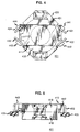
- a magnetic component 401 adapted to use windings such as shown in FIGS. 1, 2 and 3 is shown in a plan view in FIG. 4.
- An elevation depicting the component mounted on a circuit substrate 405 is shown in FIG. 5.
- a bobbin 410 supports at least a first sheet winding 411 and includes a pinout arrangement including the pins 421-424 for facilitating the interconnection of the sheet winding patterns to each other to form a desired winding and to further facilitate connecting the windings to circuitry on the circuit board or substrate 405 on which the component 401 is to be mounted.
- These pins shown in FIG. 4 are not fully reproduced in FIG. 5 so that the view presented is not unduly cluttered.
- the bobbin 410 includes four support members 441-444 which rest on the circuit board 405 and hence provide support for the component. As shown, the support members 441-444 permit the mounting of the component in an aperture or opening in the circuit substrate so that the component has approximately half of its height below the top surface of the circuit substrate 405, thereby maintaining a low profile for the component 401.
- the magnetic core 420 in the illustrative example is made of a ferrite material and comprises two component parts; a base structure 418 and a cover structure 419.
- the invention is not limited to this ferrite magnetic core material since many alternatives will be obvious to those skilled in the art.
- the core windows, 431 and 432 through which the windings pass, have a path or route comprising a circular segment.
- the inner and outer radii of these circular segments defining the windows are closely matched to the inner and outer radii of the sheet winding patterns so that they substantially fill the windows.
- FIG. 8 A perspective view of the bobbin structure is shown in FIG. 8. It includes a base member 801 with support members 802-805 for supporting the magnetic component on the circuit substrate adjacent the substrate opening.
- Conductive pins 811-820 are included in the bobbin at each end.
- Pins 811-814 are U shaped and are moulded into the bobbin so as to be adapted for facilitating interconnection of winding pattern sheets with a circuit path on the circuit substrate.
- the inner pins 816-820 are for interconnecting the winding pattern sheets to each other in order to form a winding. While a particular number and position of pins is presented in FIG. 9, it is to be understood that many other various pin arrangements are possible.
- Each of the pins has at least one exposed end positioned on the loci of a circle having a radius equal to the radius R shown in FIGS 1, 2 and 3 so that the pins and connecting holes in the sheet winding patterns are in dimension register.
- FIG. 6 An understanding of the interconnection of the sheet winding patterns to the bobbin and to each other in order to form a winding can be readily ascertained by reference to the exploded perspective view of FIG. 6.
- the magnetic core components are omitted from this view in order to facilitate the understanding of the interconnection arrangement.
- a four to one winding ratio for a transformer component is disclosed in FIG. 6 as an illustrative embodiment. It is to be understood that the invention is not limited to this particular combination. Many other arrangements for both transformer and inductor components are available.
- FIG. 6 A particular interconnection arrangement of the winding sheet patterns 631-635 in order to form a first winding is shown in FIG. 6.
- the bottom sheet winding pattern 631 has its terminal end connecting holes placed over adjacent pins 611 and 616.
- Pin 611 is a U shaped pin molded into the bobbin 601 having a terminal end 671 (shown truncated) to facilitate connecting the sheet winding pattern 631 to external circuitry.
- Pin 616 is an internal pin to facilitate the connection of sheet winding action 631 to a subsequent sheet winding pattern 632.
- the next winding sheet pattern 632 has its terminal end connecting holes placed over adjacent pins 616 and 617.
- a subsequent winding sheet pattern 633 has its terminal end connecting holes placed over adjacent pins 617 and 618.
- the next layered winding sheet pattern 634 has its terminal end connecting holes placed over an inner end of the U shaped pins 613 and 614.
- the outer terminal ends 673 and 674 connect the sheet winding pattern 634 to external circuitry.
- Pattern 634 represents a distinct single turn winding.
- the final winding sheet pattern 635 has its terminal end connecting holes placed over adjacent pins 618 and 612. The external end 672 and pin 612 are connected to the circuit board.
- sheet winding patterns 631, 632, 633 and 635 are connected electrically in series and form a first transformer winding and that sheet winding pattern 634 is an independent second winding magnetically coupled to the first winding. Continuity between individual winding patterns is provided through the pin connections with each winding pattern. Connection of a winding to the circuitry of the circuit board is via the outer extension 671-674 at the U shaped pins 611-614.
- FIG. 7 Mounting of the magnetic component on the circuit board or substrate 701 is shown in FIG. 7.
- the outer extension ends of the connecting U shaped pins 711-714 are connected to through holes in the circuit substrate 701.
- the four support members 721-724 of the bobbin 720 rest on the surface of the circuit substrate and the magnetic core 740 fits partially through an opening 702 in the circuit substrate 701, so that a low profile may be achieved.
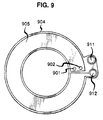
- FIG. 9 Another construction of a sheet winding pattern is disclosed in FIG. 9.
- the pattern disclosed therein comprises a copper pattern 905 etched on a thin flexible substrate 904 having copper plated through holes 901 and 902.
- the plated through holes 901 and 902 permit the coupling of two stacked winding patterns.
- Many additional windings may be devised to achieve additional multiple turn winding constructions.
- FIG. 9 a two turn winding with identical copper patterns on both the top side (shown) and the bottom side of the flexible substrate is disclosed.
- the individual windings are connected through the plated through holes 901 and 902.
- the first winding is applied to the underside of the flex substrate and connected to pin hole 911.
- This underside copper pattern is connected to the top copper pattern 905 via the plated through holes 901 and 902.
- the output of the two turn arrangement is via the pin hole 912.1.
Landscapes
- Engineering & Computer Science (AREA)
- Power Engineering (AREA)
- Coils Of Transformers For General Uses (AREA)
- Coils Or Transformers For Communication (AREA)
Claims (2)
- Magnetkomponentenausbildung mit einem Schaltungssubstrat (701) zur Aufnahme von magnetischen Bauteilen und mit einer Mehrzahl von Durchgangsbohrungen zur Aufnahme von Stiftverbindungen, wobei eine Magnetkomponente (401) folgendes umfaßt:
einen Kern aus magnetischem Material (420, 740) mit ersten und zweiten Fenstern (431, 432) mit einem kreisförmigen Weg für Windungen, die die ersten und zweiten Fenster durchqueren,
mindestens eine erste und eine zweite Windung (101, 201, 301, 631, 632) aus einer leitenden Schicht oder aus Blech, die in dem ersten und zweiten Fenster in Schichten angebracht sind und ein kreisförmiges Profil aufweisen sowie im wesentlichen das erste und das zweite Fenster ausfüllen; eine Trägerspule (410, 601, 720) umfassend
einen mittigen offenen Bereich mit einer flachen, ebenen Trägerebene zur Aufnahme des Kerns des magnetischen Materials und die ersten und zweiten Schichtwindungen, welche die ersten und zweiten Fenster durchqueren,
dadurch gekennzeichnet,
daß das Schaltungssubstrat eine Öffnung (702) aufweist, um einer montierten magnetischen Komponente zu ermöglichen, eine Ebene des Schaltungssubstrats zu durchdringen;
daß die magnetische Komponente innerhalb der Öffnung angeordnet ist, wobei ein Teil der magnetischen Komponente oberhalb der Ebene des Schaltungssubstrats zu liegen kommt, daß die leitenden Schichtwindungen jeweils erste und zweite Anschlußenden (102, 103, 202, 203) aufweisen, von denen mindestens eines eine passende Bohrung besitzt, um das Durchdringen eines leitenden Stifts und die Verbindung mit diesem zu akzeptieren,
daß eine Mehrzahl von Verbindungsstiften erster Art und zweiter Art vorgesehen sind, wobei die Verbindungsstifte der ersten Art (616) zur Verbindung der ersten und zweiten Schichtwindungen vorgesehen sind, indem sie durch die Bohrungen der Schichtwindungen hindurchreichen, und die zweite Art der Verbindungsstifte (711-712) mit ausgewählten Verbindungsstiften der ersten Art elektrisch verbunden und zur Einfügung in die Durchgangsbohrungen angeordnet sind, um die Windungen mit dem Schaltungssubstrat elektrisch zu verbinden, und
daß eine Mehrzahl von Trägerelementen (721, 724) außerhalb des äußeren Randes des Kerns angeordnet sind und auf Teilen des Schaltungssubstrats benachbart des Randes der Öffnung ruhen, um die Spule und ihren zugeordneten Kern aus magnetischem Material sowie die ersten und zweiten Schichtwindungen in der Struktur mit dem Schaltungssubstrat zu stützen. - Magnetische Komponentenstruktur nach Anspruch 1, bei der das jeweilige erste oder zweite Klemmenanschlußende der ersten und zweiten Schichtwindungen mit einem gemeinsamen Verbindungsstift erster Art verbunden ist, so daß die ersten und zweiten Schichtwindungen in Serie verbunden sind, um eine Wicklung mit mehreren Windungen zu bilden.
Applications Claiming Priority (2)
| Application Number | Priority Date | Filing Date | Title |
|---|---|---|---|
| US07/459,037 US5179365A (en) | 1989-12-29 | 1989-12-29 | Multiple turn low profile magnetic component using sheet windings |
| US459037 | 1989-12-29 |
Publications (3)
| Publication Number | Publication Date |
|---|---|
| EP0435461A2 EP0435461A2 (de) | 1991-07-03 |
| EP0435461A3 EP0435461A3 (en) | 1991-09-11 |
| EP0435461B1 true EP0435461B1 (de) | 1995-01-18 |
Family
ID=23823143
Family Applications (1)
| Application Number | Title | Priority Date | Filing Date |
|---|---|---|---|
| EP90312879A Expired - Lifetime EP0435461B1 (de) | 1989-12-29 | 1990-11-27 | Niedrigprofil-Magnetkomponente mit mehreren Schichtwindungen |
Country Status (4)
| Country | Link |
|---|---|
| US (1) | US5179365A (de) |
| EP (1) | EP0435461B1 (de) |
| JP (1) | JPH04113605A (de) |
| DE (1) | DE69016187T2 (de) |
Cited By (3)
| Publication number | Priority date | Publication date | Assignee | Title |
|---|---|---|---|---|
| EP0522475A1 (de) * | 1991-07-10 | 1993-01-13 | ABBPATENT GmbH | Induktives Bauelement und Verfahren zu seiner Herstellung |
| US5886610A (en) * | 1996-07-17 | 1999-03-23 | Canova; Antonio | Ultra flat magnetic device for electronic circuits |
| US6636140B2 (en) | 2000-12-08 | 2003-10-21 | Sansha Electric Manufacturing Company, Limited | High-frequency large current handling transformer |
Families Citing this family (55)
| Publication number | Priority date | Publication date | Assignee | Title |
|---|---|---|---|---|
| DE9211148U1 (de) * | 1992-08-20 | 1993-02-25 | Zink, Manfred, 77723 Gengenbach | Hochfrequenz-Leistungstransformator |
| US5345670A (en) * | 1992-12-11 | 1994-09-13 | At&T Bell Laboratories | Method of making a surface-mount power magnetic device |
| EP0608127A1 (de) * | 1993-01-22 | 1994-07-27 | AT&T Corp. | Isolierungsanordnung für Magnetwindungen mit gestapelten flachen Leitern |
| US5559487A (en) * | 1994-05-10 | 1996-09-24 | Reltec Corporation | Winding construction for use in planar magnetic devices |
| EP0689214B1 (de) * | 1994-06-21 | 1999-09-22 | Sumitomo Special Metals Co., Ltd. | Herstellungsverfahren für Substrat mit mehrschichtigen gedruckten Spulen |
| EP0741396A1 (de) * | 1995-05-04 | 1996-11-06 | AT&T IPM Corp. | Magnetische Leistungsvorrichtung mit drahtlose Leiterplattenanschluss und ihr Herstellungsverfahren |
| EP0741395A1 (de) | 1995-05-04 | 1996-11-06 | AT&T IPM Corp. | Anschluss-montierbare planare magnetischen Vorrichtung und ihr Herstellungsverfahren |
| US6160467A (en) * | 1995-08-09 | 2000-12-12 | Visteon Global Technologies, Inc. | Transformer with center tap |
| US5631822A (en) * | 1995-08-24 | 1997-05-20 | Interpoint Corporation | Integrated planar magnetics and connector |
| US5777539A (en) * | 1995-09-27 | 1998-07-07 | International Business Machines Corporation | Inductor using multilayered printed circuit board for windings |
| DE19629067A1 (de) * | 1996-07-18 | 1998-01-22 | Rene Weiner | Spulenkörper für eine Flachspule |
| US6073339A (en) * | 1996-09-20 | 2000-06-13 | Tdk Corporation Of America | Method of making low profile pin-less planar magnetic devices |
| DE19746919A1 (de) * | 1997-10-24 | 1999-05-06 | Daimler Chrysler Ag | Elektrische Übertragungsvorrichtung |
| US6114932A (en) * | 1997-12-12 | 2000-09-05 | Telefonaktiebolaget Lm Ericsson | Inductive component and inductive component assembly |
| DE29722005U1 (de) * | 1997-12-15 | 1998-02-12 | Schiller electronik GmbH, 76307 Karlsbad | Induktives Bauglied |
| US6087922A (en) * | 1998-03-04 | 2000-07-11 | Astec International Limited | Folded foil transformer construction |
| DE19818673A1 (de) * | 1998-04-27 | 1999-10-28 | Thomson Brandt Gmbh | Spule |
| US6222437B1 (en) | 1998-05-11 | 2001-04-24 | Nidec America Corporation | Surface mounted magnetic components having sheet material windings and a power supply including such components |
| US6046662A (en) * | 1998-09-29 | 2000-04-04 | Compaq Computer Corporation | Low profile surface mount transformer |
| US6060974A (en) * | 1998-09-29 | 2000-05-09 | Compag Computer Corporation | Header plate for a low profile surface mount transformer |
| US6420953B1 (en) | 2000-05-19 | 2002-07-16 | Pulse Engineering. Inc. | Multi-layer, multi-functioning printed circuit board |
| US7193497B2 (en) * | 2000-10-31 | 2007-03-20 | Delta Electronics Inc. | Ignition coil |
| TW470202U (en) * | 2000-10-31 | 2001-12-21 | Delta Electronics Inc | Ignition coil |
| US6628531B2 (en) * | 2000-12-11 | 2003-09-30 | Pulse Engineering, Inc. | Multi-layer and user-configurable micro-printed circuit board |
| WO2002071422A1 (en) * | 2001-03-05 | 2002-09-12 | Tdk Corporation | Planar coil and planar transformer |
| DE10148133A1 (de) * | 2001-09-28 | 2003-04-24 | Ascom Energy Systems Ag Bern | Flachtransformator mit gesteckten Sekundärwicklungen |
| US9490063B2 (en) * | 2003-02-26 | 2016-11-08 | Analogic Corporation | Shielded power coupling device |
| CN101171652B (zh) * | 2005-05-03 | 2014-03-05 | 皇家飞利浦电子股份有限公司 | 用于平面型变压器和感应器的绕组装置 |
| US7439839B2 (en) * | 2006-01-30 | 2008-10-21 | Nemic-Lambda Ltd. | High-current electrical coil, and transformer construction including same |
| TW200832460A (en) * | 2007-01-31 | 2008-08-01 | Delta Electronics Inc | Transformer structure |
| ATE554487T1 (de) | 2007-03-19 | 2012-05-15 | Abc Taiwan Electronics Corp | Unabhängiger planarer transformator |
| US7332993B1 (en) | 2007-04-10 | 2008-02-19 | Bose Corporation | Planar transformer having fractional windings |
| US8624699B2 (en) | 2009-11-09 | 2014-01-07 | Nucleus Scientific, Inc. | Electric coil and method of manufacture |
| US8585062B2 (en) | 2009-11-09 | 2013-11-19 | Nucleus Scientific, Inc. | Tunable pneumatic suspension |
| US8519575B2 (en) | 2009-11-09 | 2013-08-27 | Nucleus Scientific, Inc. | Linear electric machine with linear-to-rotary converter |
| US8362660B2 (en) | 2009-11-09 | 2013-01-29 | Nucleus Scientific, Inc. | Electric generator |
| ES2711352T3 (es) | 2010-06-11 | 2019-05-03 | Ricoh Co Ltd | Dispositivo de almacenamiento de información, dispositivo extraíble, contenedor de revelador y aparato de formación de imágenes |
| US8441331B2 (en) * | 2011-03-16 | 2013-05-14 | Delphi Technologies, Inc. | Planar magnetic structure |
| US8766493B2 (en) | 2011-07-01 | 2014-07-01 | Nucleus Scientific, Inc. | Magnetic stator assembly |
| US20130063234A1 (en) * | 2011-07-07 | 2013-03-14 | Hypertherm, Inc. | High power inductor and ignition transformer using planar magnetics |
| CN102610378A (zh) * | 2012-02-07 | 2012-07-25 | 深圳麦格米特电气股份有限公司 | 一种开关电源的平板变压器 |
| US9378885B2 (en) * | 2012-03-27 | 2016-06-28 | Pulse Electronics, Inc. | Flat coil windings, and inductive devices and electronics assemblies that utilize flat coil windings |
| JP6364765B2 (ja) * | 2012-12-27 | 2018-08-01 | Tdk株式会社 | 巻線部品 |
| NL2011129C2 (nl) | 2013-07-09 | 2015-01-12 | Eco Logical Entpr B V | Compacte elektrische inrichting en daarop gebaseerde elektrodynamische luidspreker, elektromotor, roerinrichting en instelbare koppeling. |
| CN103632812B (zh) * | 2013-12-14 | 2015-11-18 | 芜湖科伟兆伏电子有限公司 | 一种大电流高频平面电感及其制作方法 |
| TWI462129B (zh) | 2013-12-19 | 2014-11-21 | Delta Electronics Inc | 變壓器組合結構及其承座 |
| US10062497B2 (en) * | 2014-02-17 | 2018-08-28 | Honeywell International Inc. | Pseudo edge-wound winding using single pattern turn |
| CN104980003B (zh) * | 2014-04-01 | 2017-10-10 | 台达电子企业管理(上海)有限公司 | 电源模块及pol电源模块 |
| NL2013277B1 (nl) * | 2014-07-30 | 2016-09-21 | Compact Electro-Magnetic Tech And Eco-Logical Entpr B V | Elektrische inrichting, in het bijzonder een spoel of een transformator. |
| NL2013278B1 (nl) * | 2014-07-30 | 2016-07-22 | Compact Electro-Magnetic Tech And Eco-Logical Entpr B V | Werkwijze voor het vervaardigen van een elektrische inrichting, alsmede met die werkwijze verkregen inrichting. |
| JP6502056B2 (ja) * | 2014-10-22 | 2019-04-17 | 日本圧着端子製造株式会社 | 電気的接続装置 |
| US10062496B2 (en) | 2015-02-26 | 2018-08-28 | Lear Corporation | Planar transformer |
| WO2018052876A1 (en) | 2016-09-13 | 2018-03-22 | Nucleus Scientific, Inc. | Multi-bar linkage electric drive system |
| EP3563646B1 (de) | 2016-12-30 | 2025-06-11 | Eagle Harbor Technologies, Inc. | Induktiver hochspannungsaddierer |
| KR102424223B1 (ko) * | 2020-08-31 | 2022-07-25 | (주) 트랜스온 | 트랜스포머용 프라이머리 코일 어셈블리 및 이를 포함하는 트랜스포머 |
Family Cites Families (12)
| Publication number | Priority date | Publication date | Assignee | Title |
|---|---|---|---|---|
| US3004230A (en) * | 1956-10-12 | 1961-10-10 | American Mach & Foundry | Electric inductor devices |
| US3287795A (en) * | 1964-06-05 | 1966-11-29 | Western Electric Co | Methods of assembling electrical components with circuits |
| CA938356A (en) * | 1970-07-07 | 1973-12-11 | Sato Ryoda | Transformer |
| US3832661A (en) * | 1971-11-29 | 1974-08-27 | R Sato | Transformer |
| JPS5428067A (en) * | 1977-08-04 | 1979-03-02 | Kurita Water Ind Ltd | Apparatus for treating sludge-like material |
| GB2035706B (en) * | 1978-11-09 | 1983-05-05 | Tdk Electronics Co Ltd | Inductance element |
| FR2476898B1 (fr) * | 1980-02-22 | 1985-06-28 | Mini Informatiq System Ste Eur | Bobinage electromagnetique comportant des elements discrets et dispositif d'alimentation electrique comportant de tels bobinages |
| CA1202383A (en) * | 1983-03-25 | 1986-03-25 | Herman R. Person | Thick film delay line |
| US4583068A (en) * | 1984-08-13 | 1986-04-15 | At&T Bell Laboratories | Low profile magnetic structure in which one winding acts as support for second winding |
| GB2163603A (en) * | 1984-08-25 | 1986-02-26 | Stc Plc | Miniature transformer or choke |
| US4616205A (en) * | 1985-03-08 | 1986-10-07 | At&T Bell Laboratories | Preformed multiple turn transformer winding |
| EP0212609B1 (de) * | 1985-08-22 | 1989-05-17 | Siemens Aktiengesellschaft | Elektrische Spule |
-
1989
- 1989-12-29 US US07/459,037 patent/US5179365A/en not_active Expired - Lifetime
-
1990
- 1990-11-27 DE DE69016187T patent/DE69016187T2/de not_active Expired - Fee Related
- 1990-11-27 EP EP90312879A patent/EP0435461B1/de not_active Expired - Lifetime
- 1990-12-20 JP JP2412423A patent/JPH04113605A/ja active Pending
Cited By (3)
| Publication number | Priority date | Publication date | Assignee | Title |
|---|---|---|---|---|
| EP0522475A1 (de) * | 1991-07-10 | 1993-01-13 | ABBPATENT GmbH | Induktives Bauelement und Verfahren zu seiner Herstellung |
| US5886610A (en) * | 1996-07-17 | 1999-03-23 | Canova; Antonio | Ultra flat magnetic device for electronic circuits |
| US6636140B2 (en) | 2000-12-08 | 2003-10-21 | Sansha Electric Manufacturing Company, Limited | High-frequency large current handling transformer |
Also Published As
| Publication number | Publication date |
|---|---|
| DE69016187D1 (de) | 1995-03-02 |
| US5179365A (en) | 1993-01-12 |
| EP0435461A2 (de) | 1991-07-03 |
| JPH04113605A (ja) | 1992-04-15 |
| DE69016187T2 (de) | 1995-05-18 |
| EP0435461A3 (en) | 1991-09-11 |
Similar Documents
| Publication | Publication Date | Title |
|---|---|---|
| EP0435461B1 (de) | Niedrigprofil-Magnetkomponente mit mehreren Schichtwindungen | |
| US5300911A (en) | Monolithic magnetic device with printed circuit interconnections | |
| US5321380A (en) | Low profile printed circuit board | |
| US5565837A (en) | Low profile printed circuit board | |
| US4583068A (en) | Low profile magnetic structure in which one winding acts as support for second winding | |
| US4689023A (en) | Programmable electrical connector | |
| US6073339A (en) | Method of making low profile pin-less planar magnetic devices | |
| US5801611A (en) | Inductive device | |
| US4547961A (en) | Method of manufacture of miniaturized transformer | |
| US5402098A (en) | Coil | |
| CA1177127A (en) | Miniaturized transformer construction | |
| US5479146A (en) | Pot core matrix transformer having improved heat rejection | |
| US6380834B1 (en) | Planar magnetic assembly | |
| US5402321A (en) | Composite device having inductor and coupling member | |
| US6844804B2 (en) | Method of manufacturing discrete electronic components | |
| US5694104A (en) | Low profile high power surface mount transformer | |
| JP3598405B2 (ja) | プリントコイル部品及びプリントコイル基板 | |
| JP3513623B2 (ja) | 固定子 | |
| JPH088180B2 (ja) | 基板実装用小型変成器 | |
| JPH0653055A (ja) | 導電体と導電ランで構成された電磁巻線 | |
| WO1998054733A2 (en) | Low profile pin-less planar magnetic devices and method of making same | |
| JPS6119109A (ja) | トランス | |
| GB2308923A (en) | Transformer winding structure | |
| JPH0737290Y2 (ja) | 端子台を備えたコイル装置 | |
| EP0795184A2 (de) | Planerer impulstransformator |
Legal Events
| Date | Code | Title | Description |
|---|---|---|---|
| PUAI | Public reference made under article 153(3) epc to a published international application that has entered the european phase |
Free format text: ORIGINAL CODE: 0009012 |
|
| AK | Designated contracting states |
Kind code of ref document: A2 Designated state(s): DE FR GB IT |
|
| PUAL | Search report despatched |
Free format text: ORIGINAL CODE: 0009013 |
|
| AK | Designated contracting states |
Kind code of ref document: A3 Designated state(s): DE FR GB IT |
|
| 17P | Request for examination filed |
Effective date: 19920221 |
|
| 17Q | First examination report despatched |
Effective date: 19930909 |
|
| RAP3 | Party data changed (applicant data changed or rights of an application transferred) |
Owner name: AT&T CORP. |
|
| GRAA | (expected) grant |
Free format text: ORIGINAL CODE: 0009210 |
|
| AK | Designated contracting states |
Kind code of ref document: B1 Designated state(s): DE FR GB IT |
|
| REF | Corresponds to: |
Ref document number: 69016187 Country of ref document: DE Date of ref document: 19950302 |
|
| ET | Fr: translation filed | ||
| ITF | It: translation for a ep patent filed | ||
| PLBE | No opposition filed within time limit |
Free format text: ORIGINAL CODE: 0009261 |
|
| STAA | Information on the status of an ep patent application or granted ep patent |
Free format text: STATUS: NO OPPOSITION FILED WITHIN TIME LIMIT |
|
| 26N | No opposition filed | ||
| REG | Reference to a national code |
Ref country code: GB Ref legal event code: IF02 |
|
| PGFP | Annual fee paid to national office [announced via postgrant information from national office to epo] |
Ref country code: FR Payment date: 20021023 Year of fee payment: 13 |
|
| PGFP | Annual fee paid to national office [announced via postgrant information from national office to epo] |
Ref country code: GB Payment date: 20021029 Year of fee payment: 13 |
|
| PGFP | Annual fee paid to national office [announced via postgrant information from national office to epo] |
Ref country code: DE Payment date: 20021205 Year of fee payment: 13 |
|
| PG25 | Lapsed in a contracting state [announced via postgrant information from national office to epo] |
Ref country code: GB Free format text: LAPSE BECAUSE OF NON-PAYMENT OF DUE FEES Effective date: 20031127 |
|
| PG25 | Lapsed in a contracting state [announced via postgrant information from national office to epo] |
Ref country code: DE Free format text: LAPSE BECAUSE OF NON-PAYMENT OF DUE FEES Effective date: 20040602 |
|
| GBPC | Gb: european patent ceased through non-payment of renewal fee |
Effective date: 20031127 |
|
| PG25 | Lapsed in a contracting state [announced via postgrant information from national office to epo] |
Ref country code: FR Free format text: LAPSE BECAUSE OF NON-PAYMENT OF DUE FEES Effective date: 20040730 |
|
| REG | Reference to a national code |
Ref country code: FR Ref legal event code: ST |
|
| PG25 | Lapsed in a contracting state [announced via postgrant information from national office to epo] |
Ref country code: IT Free format text: LAPSE BECAUSE OF NON-PAYMENT OF DUE FEES Effective date: 20051127 |