EP0436300A2 - Analoges optisches Faser-Kommunikationssystem und zum Gebrauch in einem solchen System angepasster Laser - Google Patents
Analoges optisches Faser-Kommunikationssystem und zum Gebrauch in einem solchen System angepasster Laser Download PDFInfo
- Publication number
- EP0436300A2 EP0436300A2 EP90312936A EP90312936A EP0436300A2 EP 0436300 A2 EP0436300 A2 EP 0436300A2 EP 90312936 A EP90312936 A EP 90312936A EP 90312936 A EP90312936 A EP 90312936A EP 0436300 A2 EP0436300 A2 EP 0436300A2
- Authority
- EP
- European Patent Office
- Prior art keywords
- laser
- cavity
- lasers
- current
- facet
- Prior art date
- Legal status (The legal status is an assumption and is not a legal conclusion. Google has not performed a legal analysis and makes no representation as to the accuracy of the status listed.)
- Granted
Links
Images


Classifications
-
- H—ELECTRICITY
- H01—ELECTRIC ELEMENTS
- H01S—DEVICES USING THE PROCESS OF LIGHT AMPLIFICATION BY STIMULATED EMISSION OF RADIATION [LASER] TO AMPLIFY OR GENERATE LIGHT; DEVICES USING STIMULATED EMISSION OF ELECTROMAGNETIC RADIATION IN WAVE RANGES OTHER THAN OPTICAL
- H01S5/00—Semiconductor lasers
- H01S5/10—Construction or shape of the optical resonator, e.g. extended or external cavity, coupled cavities, bent-guide, varying width, thickness or composition of the active region
- H01S5/12—Construction or shape of the optical resonator, e.g. extended or external cavity, coupled cavities, bent-guide, varying width, thickness or composition of the active region the resonator having a periodic structure, e.g. in distributed feedback [DFB] lasers
-
- H—ELECTRICITY
- H04—ELECTRIC COMMUNICATION TECHNIQUE
- H04B—TRANSMISSION
- H04B10/00—Transmission systems employing electromagnetic waves other than radio-waves, e.g. infrared, visible or ultraviolet light, or employing corpuscular radiation, e.g. quantum communication
- H04B10/50—Transmitters
- H04B10/501—Structural aspects
- H04B10/503—Laser transmitters
- H04B10/504—Laser transmitters using direct modulation
-
- H—ELECTRICITY
- H04—ELECTRIC COMMUNICATION TECHNIQUE
- H04B—TRANSMISSION
- H04B10/00—Transmission systems employing electromagnetic waves other than radio-waves, e.g. infrared, visible or ultraviolet light, or employing corpuscular radiation, e.g. quantum communication
- H04B10/50—Transmitters
- H04B10/564—Power control
-
- H—ELECTRICITY
- H04—ELECTRIC COMMUNICATION TECHNIQUE
- H04B—TRANSMISSION
- H04B10/00—Transmission systems employing electromagnetic waves other than radio-waves, e.g. infrared, visible or ultraviolet light, or employing corpuscular radiation, e.g. quantum communication
- H04B10/50—Transmitters
- H04B10/58—Compensation for non-linear transmitter output
-
- H—ELECTRICITY
- H01—ELECTRIC ELEMENTS
- H01S—DEVICES USING THE PROCESS OF LIGHT AMPLIFICATION BY STIMULATED EMISSION OF RADIATION [LASER] TO AMPLIFY OR GENERATE LIGHT; DEVICES USING STIMULATED EMISSION OF ELECTROMAGNETIC RADIATION IN WAVE RANGES OTHER THAN OPTICAL
- H01S5/00—Semiconductor lasers
- H01S5/02—Structural details or components not essential to laser action
- H01S5/028—Coatings ; Treatment of the laser facets, e.g. etching, passivation layers or reflecting layers
-
- H—ELECTRICITY
- H01—ELECTRIC ELEMENTS
- H01S—DEVICES USING THE PROCESS OF LIGHT AMPLIFICATION BY STIMULATED EMISSION OF RADIATION [LASER] TO AMPLIFY OR GENERATE LIGHT; DEVICES USING STIMULATED EMISSION OF ELECTROMAGNETIC RADIATION IN WAVE RANGES OTHER THAN OPTICAL
- H01S5/00—Semiconductor lasers
- H01S5/06—Arrangements for controlling the laser output parameters, e.g. by operating on the active medium
-
- H—ELECTRICITY
- H01—ELECTRIC ELEMENTS
- H01S—DEVICES USING THE PROCESS OF LIGHT AMPLIFICATION BY STIMULATED EMISSION OF RADIATION [LASER] TO AMPLIFY OR GENERATE LIGHT; DEVICES USING STIMULATED EMISSION OF ELECTROMAGNETIC RADIATION IN WAVE RANGES OTHER THAN OPTICAL
- H01S5/00—Semiconductor lasers
- H01S5/06—Arrangements for controlling the laser output parameters, e.g. by operating on the active medium
- H01S5/062—Arrangements for controlling the laser output parameters, e.g. by operating on the active medium by varying the potential of the electrodes
- H01S5/06209—Arrangements for controlling the laser output parameters, e.g. by operating on the active medium by varying the potential of the electrodes in single-section lasers
- H01S5/06213—Amplitude modulation
-
- H—ELECTRICITY
- H01—ELECTRIC ELEMENTS
- H01S—DEVICES USING THE PROCESS OF LIGHT AMPLIFICATION BY STIMULATED EMISSION OF RADIATION [LASER] TO AMPLIFY OR GENERATE LIGHT; DEVICES USING STIMULATED EMISSION OF ELECTROMAGNETIC RADIATION IN WAVE RANGES OTHER THAN OPTICAL
- H01S5/00—Semiconductor lasers
- H01S5/06—Arrangements for controlling the laser output parameters, e.g. by operating on the active medium
- H01S5/062—Arrangements for controlling the laser output parameters, e.g. by operating on the active medium by varying the potential of the electrodes
- H01S5/0625—Arrangements for controlling the laser output parameters, e.g. by operating on the active medium by varying the potential of the electrodes in multi-section lasers
- H01S5/06255—Controlling the frequency of the radiation
-
- H—ELECTRICITY
- H01—ELECTRIC ELEMENTS
- H01S—DEVICES USING THE PROCESS OF LIGHT AMPLIFICATION BY STIMULATED EMISSION OF RADIATION [LASER] TO AMPLIFY OR GENERATE LIGHT; DEVICES USING STIMULATED EMISSION OF ELECTROMAGNETIC RADIATION IN WAVE RANGES OTHER THAN OPTICAL
- H01S5/00—Semiconductor lasers
- H01S5/06—Arrangements for controlling the laser output parameters, e.g. by operating on the active medium
- H01S5/062—Arrangements for controlling the laser output parameters, e.g. by operating on the active medium by varying the potential of the electrodes
- H01S5/0625—Arrangements for controlling the laser output parameters, e.g. by operating on the active medium by varying the potential of the electrodes in multi-section lasers
- H01S5/06255—Controlling the frequency of the radiation
- H01S5/06258—Controlling the frequency of the radiation with DFB-structure
-
- H—ELECTRICITY
- H01—ELECTRIC ELEMENTS
- H01S—DEVICES USING THE PROCESS OF LIGHT AMPLIFICATION BY STIMULATED EMISSION OF RADIATION [LASER] TO AMPLIFY OR GENERATE LIGHT; DEVICES USING STIMULATED EMISSION OF ELECTROMAGNETIC RADIATION IN WAVE RANGES OTHER THAN OPTICAL
- H01S5/00—Semiconductor lasers
- H01S5/10—Construction or shape of the optical resonator, e.g. extended or external cavity, coupled cavities, bent-guide, varying width, thickness or composition of the active region
-
- H—ELECTRICITY
- H01—ELECTRIC ELEMENTS
- H01S—DEVICES USING THE PROCESS OF LIGHT AMPLIFICATION BY STIMULATED EMISSION OF RADIATION [LASER] TO AMPLIFY OR GENERATE LIGHT; DEVICES USING STIMULATED EMISSION OF ELECTROMAGNETIC RADIATION IN WAVE RANGES OTHER THAN OPTICAL
- H01S5/00—Semiconductor lasers
- H01S5/10—Construction or shape of the optical resonator, e.g. extended or external cavity, coupled cavities, bent-guide, varying width, thickness or composition of the active region
- H01S5/12—Construction or shape of the optical resonator, e.g. extended or external cavity, coupled cavities, bent-guide, varying width, thickness or composition of the active region the resonator having a periodic structure, e.g. in distributed feedback [DFB] lasers
- H01S5/124—Construction or shape of the optical resonator, e.g. extended or external cavity, coupled cavities, bent-guide, varying width, thickness or composition of the active region the resonator having a periodic structure, e.g. in distributed feedback [DFB] lasers incorporating phase shifts
-
- H—ELECTRICITY
- H01—ELECTRIC ELEMENTS
- H01S—DEVICES USING THE PROCESS OF LIGHT AMPLIFICATION BY STIMULATED EMISSION OF RADIATION [LASER] TO AMPLIFY OR GENERATE LIGHT; DEVICES USING STIMULATED EMISSION OF ELECTROMAGNETIC RADIATION IN WAVE RANGES OTHER THAN OPTICAL
- H01S5/00—Semiconductor lasers
- H01S5/10—Construction or shape of the optical resonator, e.g. extended or external cavity, coupled cavities, bent-guide, varying width, thickness or composition of the active region
- H01S5/12—Construction or shape of the optical resonator, e.g. extended or external cavity, coupled cavities, bent-guide, varying width, thickness or composition of the active region the resonator having a periodic structure, e.g. in distributed feedback [DFB] lasers
- H01S5/124—Construction or shape of the optical resonator, e.g. extended or external cavity, coupled cavities, bent-guide, varying width, thickness or composition of the active region the resonator having a periodic structure, e.g. in distributed feedback [DFB] lasers incorporating phase shifts
- H01S5/1243—Construction or shape of the optical resonator, e.g. extended or external cavity, coupled cavities, bent-guide, varying width, thickness or composition of the active region the resonator having a periodic structure, e.g. in distributed feedback [DFB] lasers incorporating phase shifts by other means than a jump in the grating period, e.g. bent waveguides
Definitions
- This invention pertains to optical multichannel analog communications systems, and to semiconductor lasers adapted for use in such systems.
- the wide bandwidths of semiconductor laser diodes and optical fibers make analog sub-carrier modulation an attractive technology.
- Several signals at different sub-carrier frequencies each signal representing one of the television channels to be multiplexed, are summed and applied concurrently to the input of the laser device.
- the input information signal is a set of frequency-modulated sub-carriers at different frequencies, e.g., frequencies ⁇ 0, ⁇ 1, ⁇ 2, ............ .
- the resulting laser injection current comprises a dc bias level plus the set of frequency-modulated sub-carrier signals.
- the magnitude of the optical output power from the laser fluctuates with the magnitude of the laser injection current.
- the resulting sub-carrier frequency division multiplexed (FDM) optical output signal is applied to an optical fiber for transmission over an extended distance.
- the optical signal is detected by appropriate means, e.g., a PIN diode, and the resulting electrical signal is processed by conventional means to recover the individual signals. See, for instance, R. Olshansky et al., Electronics Letters, Vol. 23(22), pp. 1196-1197(1987).
- Multi-channel amplitude modulated signal transmission requires special limitations on the power, the non-linearity, and the intensity noise of the transmitting laser diode.
- laser output light intensity must be a very nearly linear function of the laser drive current under large-signal modulation.
- Strict limitations on laser nonlinearity are required because of the wide dynamic range of the National Television Systems Committee (NTSC) standard video format.
- NTSC National Television Systems Committee
- the ratio of the magnitude of the carrier to the magnitude of the total third order intermodulation distortion products at the carrier frequency must be less than -60 dBc.
- the peak second-order distortion i.e., the sum of several tens of two-tone products (or the ratio of the carrier to the largest composite second-order peak) must be less than -60 dBc.
- the transmitting laser light-versus-current characteristic must be extremely linear.
- any nonlinearity in the laser diode characteristic will result in intermodulation noise.
- Laser nonlinearities create energy transfers from the applied sub-carrier frequencies to, among others, those frequencies that are the sum and difference frequencies of all of the pairs of applied signal frequencies. Such energy transfers cause undesirable intermodulation distortion and interference, both of which can limit the performance of the transmission system.
- Nonlinearity there are several known causes of nonlinearity in semiconductor laser diodes. Some of the causes of nonlinearity are high frequency relaxation oscillations, low frequency heating effects, damping mechanisms, optical modulation depth, leakage current, gain compression, and nonlinear absorption. The resulting effect of the distortion and interference is a degradation in the signal-to-noise ratio for the signal, as received further along in the system.
- An experimental sub-carrier frequency division multiplexed, optical communication system having sixty frequency-modulated channels in the 2 GHz to 8 GHz band has been operated with a 56 dB weighted signal-to-noise ratio.
- Other arrangements using microwave carriers for subscriber loop transmission have put (1) five frequency-modulated video channels in the 150 MHz to 300 MHz band and (2) ten frequency-modulated video channels in a C-band satellite signal in the 4.9 GHz to 5.2 GHz band.
- DFB laser design has previously been considered with a view towards optimizing performance of such lasers in digital applications, including coherent optical fiber transmission systems.
- This work generally aimed at, inter alia, relatively high slope efficiency ("slope efficiency” is defined herein as the maximum value of dL/dI of the laser, where L is the radiation output power at the front facet of the laser, and I is the laser drive current) and, consequently, relatively high output power asymmetry between the front and back facets of the lasers.
- slope efficiency is defined herein as the maximum value of dL/dI of the laser, where L is the radiation output power at the front facet of the laser, and I is the laser drive current
- Other important design criteria for digital laser applications include spectral purity (or "side mode suppression ratio"), chirp, and linewidth. To optimize the performance of devices in these respects the use of various facet coatings and phase shifts have been considered.
- the invention is generally as defined by the claims.
- the invention is a multichannel analog optical fiber communication system that comprises a semiconductor laser having novel design features.
- the system comprises transmitting means, receiving means, and a length of optical fiber, signal-transmissively connecting the transmitting means and the receiving means.
- the transmitting means comprise a semiconductor laser according to the invention, having features that are discussed below.
- the operation of the system comprises causing a current of predetermined value to flow through the laser, and varying the current in response to an external signal, such that L varies in response to the external signal.
- the current has a dc component corresponding to the operating point of the diode on the L-I curve, and an ac component superimposed on the dc component.
- the operating point is selected at or near the current value (herein designated I op ) at which dL/dI is a maximum.
- the invention is a semiconductor laser having novel design features. These features can increase the likelihood that a given laser will have characteristics such that it is acceptable for use in a multichannel analog fiber communication system.
- lasers according to the invention are expected to find advantageous use also in other applications that can benefit from low distortion, and all such uses are contemplated.
- lasers according to the invention comprise a semiconductor body that forms a laser cavity of length L that is defined by a front facet and a back facet (the "front” of the cavity is the side from which the useful radiation is emitted, and the “back” is the opposite side).
- a reflectivity Associated with each of the facets is a reflectivity, and associated with the cavity (and any given portion thereof) is, during operation of the laser, a photon density and a gain (by “operation” of the laser we mean above-threshold operation).
- Lasers according to the invention also comprise a grating or other means for providing distributed feedback, and further comprise contact means that facilitate flowing an electrical current through the semiconductor body.
- the lasers furthermore comprise means adapted for producing, during operation of the laser, a non-uniform photon density in the cavity, the density of photons being larger in the back portion of the cavity than in the front portion (the "back portion” of the cavity herein is the portion that is adjacent to the back facet, and the "front portion” is the remainder of the cavity.
- the length of the back portion typically is in the approximate range L/4 to 3L/4, exemplarily about L/2).
- the non-uniform photon density is such that, during operation of the laser, the gain in the back portion of the cavity is substantially independent of the current through the semiconductor body, whereas the gain in the front portion of the cavity is a function of the current through the semiconductor body.
- Such a non-uniform photon distribution substantially enhances the likelihood that a laser according to the invention has a value of I op -I th greater than some predetermined value, e.g., greater than 10mA.
- I th is the laser threshold current, i.e., the device current at which the transition to laser oscillation occurs.
- a relatively high value of the parameter I op -I th signifies that the laser is likely to have relatively high output power at I op , and therefore is likely to be acceptable for use in a multichannel analog optical fiber communication system, or other application that requires a laser that exhibits low distortion at a relatively high output level.
- DFB lasers typically have a longitudinally varying photon distribution. See, for instance, M. Wu et al, (op. cit.).
- This phase is substantially uncontrollable and therefore typically randomly distributed, resulting in wide variation of the location of the peak between lasers, even nominally identical lasers from a given wafer.
- yield of acceptable lasers can be substantially improved. It is to be emphasized, however, that incorporation of means that favor the desired photon distribution can not insure that a given laser will have the desired distribution, due to the random phases of the wave at the facets.
- laser power asymmetry is defined herein as the ratio of front facet power to back facet power, determined at a front facet power of 4mW.
- lasers according to the invention typically will be relatively strongly coupled AR/HR DFB lasers (i.e., having an antireflection coated front facet and a high reflection coated back facet, with KL greater than about 1.6, typically in the range 1.6-2.5, with values of about 2 being currently preferred). It will be recognized that the prior art frequently aimed at values of KL ⁇ 1.5 in distributed feedback (DFB) lasers for communications use. See, for instance, C. H. Henry, (op. cit.).
- DFB distributed feedback
- the means adapted for producing the desired photon distribution also include a grating feature (conventionally called a phase shift) located in the part of the grating that is associated with the back portion of the cavity.
- the feature typically is an appropriate grating discontinuity.
- phase shifts typically were placed at the mid-point of the grating, or in the front portion of the cavity. This typically was done in combination with AR/AR coatings to maximize the spectral purity. The prior art phase shifts do not favor high photon density in the back portion of the cavity.
- Other means that favor the desired non-uniform photon distribution include split contact means, with one part of the split means being associated with the back portion of the cavity and another part being associated with the front portion of the cavity, such that the currents through the back and front portions of the cavity can be separately controlled.
- Still other means are structure means that have the effect of causing the gain in the front portion of the cavity to be relatively low, as compared to the gain in the back portion.
- Exemplary of such structure means is a cavity of non-constant width, with at least a part of the front portion of the cavity being wider than the back portion.
- FIG. 1 schematically depicts an exemplary amplitude modulated-vestigial sideband signal sub-channel multiplexed optical transmission system 10.
- Several baseband frequency modulation television channel signals 120, 121, 122 Vietnamese quarter-wavelength signals 120, 121, 122 , 12n are frequency division multiplexed on different carrier frequencies ⁇ 0, ⁇ 1, ⁇ 2 .... ⁇ n , (with n typically substantially greater than 10, e.g., about 40) as separate amplitude modulated-vestigial sideband signal sub-channels in a composite multiplex signal.
- a summer 15 combines the individual channel signals at the different sub-channel frequencies and a dc bias current I op from dc source 11 into the composite multiplex signal.
- This composite multiplex signal is applied to inventive laser diode 18 as the laser drive input signal.
- the total laser input drive signal, or injection current, to the laser diode 18 includes both the dc bias component I op and the composite multiplex signal from the summer 15.
- the channels typically are equally spaced in frequency, with the frequency width of each channel typically being in the range from 10-550 MHz, the bandwidth typically depending, inter alia, on the nature of the signal that is to be transmitted.
- the output of the laser generally is in the visible or near infrared portion of the spectrum, exemplarily in the approximate range 0.8-1.6 ⁇ m.
- the output radiation is coupled into optical fiber 13, and transmitted therethrough to receiver 14.
- DFB lasers are well known in the art and need no detailed discussion. See, for instance, J. L. Zilko et al., IEEE J. of Quantum Electronics , Vol. 25(10), pp. 2091-2095(1989). Methods of producing a phase-shift (typically a ⁇ /4 shift) are also known. See, for instance, K. Utaka, (op. cit.). Furthermore, those skilled in the art know techniques for applying AR coatings (typically reflectivity less than about 2%) and HR coatings (typically reflectivity greater than about 30%) to laser facets. Herein we consider a laser to be AR/HR if the ratio of front facet reflectivity to back facet reflectivity is less than about 5%.
- FIG. 2 shows data obtained from a laser that is not considered acceptable for use in a multichannel analog communication system, but that is potentially useful for a digital communication system.
- curve 20 is the front facet output power
- curve 21 is the back facet output power
- curve 22 is the first derivative of 20 with respect to the drive current.
- the laser had a relatively high value of laser power asymmetry (7.8), relatively low value I op -I th (8mA), and relatively high slope efficiency (0.32 mW/mA).
- FIG. 3 shows data from a laser according to the invention that is acceptable for use in a multichannel analog communication system.
- Curves 30, 31, and 32 are the front facet output power, back facet output power, and the first derivative of the front facet output power, respectively.
- the laser has relatively low power asymmetry (2.3) and relatively high value of I op -I th (17mA). It also has relatively low slope efficiency (0.24 mW/mA).
- the laser of FIG. 3 is a CMBH-DFB laser of the type described by J. L. Zilko et al., (op. cit.).
- the laser had a 65% HR coating and a ( ⁇ 1%) AR coating and KL of about 1.8.
- Lasers according to the invention optionally comprise one or more additional features that can enhance the likelihood that a given laser has the desired non-uniform photon distribution and thus is likely to be acceptable for use in an analog communication system.
- An exemplary non-uniform photon distribution according to the invention is schematically depicted in FIG. 4.
- phase shift typically by ⁇ /4 in the back portion of the grating, i.e., in the part of the grating that is associated with the back portion of the cavity.
- a phase shift allows the lasing mode to be concentrated about the phase shift. Locating the phase shift in the back portion of the grating can greatly increase the probability that the laser has a "sweet spot" (and has I op much greater than I th ), and is contrary to prior art practice, which places the phase shift into the center or the front portion of the grating.
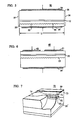
- FIG. 5 schematically depicts a AR/HR laser (50) with a phase shift located approximately 3L/4 from the front facet.
- the semiconductor body comprises active region 52 and grating 53, with the latter comprising ⁇ /4 phase shift 54.
- the front facet 55 is (completely or partially) covered with AR coating 57 and back facet 56 is (completely or partially) coated with HR coating 58.
- the laser also comprises conventional contacts 59 and 59'.
- FIG. 6 schematically shows laser 60 which comprises split contact means 61 and 62. It will be understood that such a laser may optionally comprise facet coatings and/or a phase shift (not shown).
- a current divider can be integral to the laser, or the division can be caused by external means. Also, they will recognize that the division can be in a fixed ratio or be some more complicated function. As the limiting case of the divided current, a laser can have an unpumped front portion.
- a still further feature is structural means that cause the gain in the front portion of the laser to be relatively low, as compared to the gain in the back portion.
- Exemplary structural means are a non-constant mesa width, with the front portion of the mesa being wider than the back portion. The change in width can be gradual or abrupt.
- FIG. 7 schematically depicts an exemplary laser 70 with non-constant mesa width.
- the semiconductor body comprises active region 52 and grating 53, both being part of mesa 72.
- the body also comprises semi-insulating current blocking material 73.
- the mesa is etched to comprise a relatively narrow portion adjacent to the rear facet and a relatively wide portion 74. Facet coatings are not shown.
- Example 1 A multiplicity of CMBH DFB lasers was produced substantially as described by Zilko et al. (op. cit.). The grating depth and device length were chosen to result in KL of about 1.8. Yttria stabilized zirconia coatings were applied to the facets, substantially as described in US patent 4,749,255. The coating parameters were selected to result in an AR coating ( ⁇ 1% reflectivity) on the front facets and a HR coating (about 65% reflectivity) on the back facets. Conventional electrodes were applied in a conventional manner, and a variety of measurements were carried out on the devices.
- the measurements indicate that the multiplicity of lasers according to the invention contained a higher percentage of lasers adapted for use in a multichannel analog optical fiber communication system than is present in an analogous sample of prior art CMBH DFB AR/AR lasers that have KL ⁇ 1.6.
- FIG. 3 shows measurement results from a representative member of the multiplicity of lasers. The measurements in their totality indicate that the lasers that met the specifications for the communication system had a non-uniform photon density, with the density being larger in the back portion of the cavity than in the front portion.
- Example 2 A multiplicity of lasers is produced substantially as described in Example 1, except that a ⁇ /4 phase shift is introduced into the grating in a manner substantially as taught by Utaka et al. (op. cit.). Lithography conditions are chosen to result in a phase shift location about 3L/4 from the front facet. Measurements carried out on the multiplicity of lasers yield results similar to those carried out on the lasers of Example 1.
- Example 3 A multiplicity of lasers is produced substantially as described in Example 1, except that the p-side electrode is a symmetrically split electrode.
- the split electrode is produced by lithography and etching techniques that are well known in the art. Electrical isolation between the front and back electrode segments of 2-5 k ⁇ was achieved by means substantially as described by C. Y. Kuo et al., Applied Physics Letters , Vol. 55(13), pp. 1279-1281 (1989). Injection of independent currents through the two electrode segments of a given laser made it possible to clamp the gain in the back portion of the cavity while at the same time having unclamped gain in the front portion. Measurements carried out on the multiplicity of lasers yield results similar to those carried out on the lasers of Example 1.
- Example 4 A multiplicity of lasers is produced substantially as described in Example 1, except that a mask set is used that is appropriately modified to result in mesas of the type schematically shown in FIG. 7. Conventional lithography and etching are used to produce the mesas, with the front portion of a given mesa being about double the width of the back portion. This geometrical feature results in lowered gain in the front portion of the cavity, with the gain in that portion being dependent on the laser current. Measurements carried out on the multiplicity of lasers yield results similar to those carried out on the lasers of Example 1.
Landscapes
- Physics & Mathematics (AREA)
- Electromagnetism (AREA)
- Engineering & Computer Science (AREA)
- Computer Networks & Wireless Communication (AREA)
- Signal Processing (AREA)
- Optics & Photonics (AREA)
- Nonlinear Science (AREA)
- Condensed Matter Physics & Semiconductors (AREA)
- General Physics & Mathematics (AREA)
- Semiconductor Lasers (AREA)
Applications Claiming Priority (2)
| Application Number | Priority Date | Filing Date | Title |
|---|---|---|---|
| US07/459,922 US5012484A (en) | 1990-01-02 | 1990-01-02 | Analog optical fiber communication system, and laser adapted for use in such a system |
| US459922 | 1995-06-02 |
Publications (3)
| Publication Number | Publication Date |
|---|---|
| EP0436300A2 true EP0436300A2 (de) | 1991-07-10 |
| EP0436300A3 EP0436300A3 (en) | 1992-01-15 |
| EP0436300B1 EP0436300B1 (de) | 1994-03-23 |
Family
ID=23826696
Family Applications (1)
| Application Number | Title | Priority Date | Filing Date |
|---|---|---|---|
| EP90312936A Expired - Lifetime EP0436300B1 (de) | 1990-01-02 | 1990-11-28 | Analoges optisches Faser-Kommunikationssystem und zum Gebrauch in einem solchen System angepasster Laser |
Country Status (3)
| Country | Link |
|---|---|
| US (1) | US5012484A (de) |
| EP (1) | EP0436300B1 (de) |
| DE (1) | DE69007602T2 (de) |
Cited By (2)
| Publication number | Priority date | Publication date | Assignee | Title |
|---|---|---|---|---|
| EP0579437A3 (de) * | 1992-07-17 | 1994-02-09 | AT&T Corp. | Beschichtete DFB-Halbleiterlaser für Anwendung in einem analogen optischen Faserkommunikationssystem |
| EP0588197A1 (de) * | 1992-09-07 | 1994-03-23 | Kabushiki Kaisha Toshiba | Hochleistungshalbleiterlaser mit verteilter Rückkoppelung |
Families Citing this family (16)
| Publication number | Priority date | Publication date | Assignee | Title |
|---|---|---|---|---|
| US5210631A (en) * | 1989-12-22 | 1993-05-11 | General Instrument Corporation | Transmission of AM-VSB video signals over an optical fiber |
| US5111475A (en) * | 1990-01-02 | 1992-05-05 | At&T Bell Laboratories | Analog optical fiber communication system, and laser adapted for use in such a system |
| JP2804838B2 (ja) * | 1990-10-11 | 1998-09-30 | 国際電信電話株式会社 | 波長可変半導体レーザ |
| US5241552A (en) * | 1991-10-22 | 1993-08-31 | At&T Bell Laboratories | Compensated laser structure for analog communication applications |
| US5793521A (en) * | 1992-09-21 | 1998-08-11 | Sdl Inc. | Differentially patterned pumped optical semiconductor gain media |
| US5469459A (en) * | 1993-01-08 | 1995-11-21 | Nec Corporation | Laser diode element with excellent intermodulation distortion characteristic |
| US5319666A (en) * | 1993-04-07 | 1994-06-07 | At&T Bell Laboratories | Article comprising a distributed feedback laser |
| US6501777B1 (en) * | 1999-01-29 | 2002-12-31 | Nec Corporation | Distributed feedback semiconductor laser emitting device having asymmetrical diffraction gratings |
| CA2352059A1 (en) | 1999-09-29 | 2001-04-05 | Masaki Funabashi | Gain-coupled distributed feedback type semiconductor laser device |
| US6477194B1 (en) * | 1999-11-15 | 2002-11-05 | Agere Systems Guardian Corp. | Low temperature distributed feedback laser with loss grating and method |
| JP3778260B2 (ja) * | 2000-08-16 | 2006-05-24 | 日本電気株式会社 | 半導体レーザとこれを用いたデジタル光通信システムと方法 |
| JP2005353761A (ja) * | 2004-06-09 | 2005-12-22 | Mitsubishi Electric Corp | 分布帰還型半導体レーザ |
| US7505496B2 (en) * | 2006-04-05 | 2009-03-17 | Ciena Corporation | Systems and methods for real-time compensation for non-linearity in optical sources for analog signal transmission |
| JP2008098299A (ja) | 2006-10-10 | 2008-04-24 | Mitsubishi Electric Corp | 半導体光素子及びその製造方法 |
| US8265112B2 (en) * | 2009-03-26 | 2012-09-11 | Kaiam Corp. | Semiconductor laser device and circuit for and method of driving same |
| WO2011052075A1 (ja) * | 2009-10-30 | 2011-05-05 | 富士通株式会社 | 光信号処理装置、受信機、および光ネットワークシステム |
Family Cites Families (5)
| Publication number | Priority date | Publication date | Assignee | Title |
|---|---|---|---|---|
| JPS6147685A (ja) * | 1984-08-15 | 1986-03-08 | Kokusai Denshin Denwa Co Ltd <Kdd> | 分布帰還形半導体レ−ザ |
| JPS61216383A (ja) * | 1985-03-20 | 1986-09-26 | Nec Corp | 分布帰還型半導体レ−ザ |
| US4749255A (en) * | 1985-12-09 | 1988-06-07 | American Telephone And Telegraph Company, At&T Bell Laboratories | Coating for optical devices |
| JPS63185A (ja) * | 1986-06-19 | 1988-01-05 | Fujitsu Ltd | 半導体レ−ザ |
| JP2533355B2 (ja) * | 1988-03-11 | 1996-09-11 | 国際電信電話株式会社 | 分布帰還形半導体レ―ザ装置およびその電流注入方法 |
-
1990
- 1990-01-02 US US07/459,922 patent/US5012484A/en not_active Expired - Lifetime
- 1990-11-28 DE DE69007602T patent/DE69007602T2/de not_active Expired - Lifetime
- 1990-11-28 EP EP90312936A patent/EP0436300B1/de not_active Expired - Lifetime
Cited By (3)
| Publication number | Priority date | Publication date | Assignee | Title |
|---|---|---|---|---|
| EP0579437A3 (de) * | 1992-07-17 | 1994-02-09 | AT&T Corp. | Beschichtete DFB-Halbleiterlaser für Anwendung in einem analogen optischen Faserkommunikationssystem |
| EP0588197A1 (de) * | 1992-09-07 | 1994-03-23 | Kabushiki Kaisha Toshiba | Hochleistungshalbleiterlaser mit verteilter Rückkoppelung |
| US5353298A (en) * | 1992-09-07 | 1994-10-04 | Kabushiki Kaisha Toshiba | High power distributed feedback semiconductor laser excellent in linearity of light output |
Also Published As
| Publication number | Publication date |
|---|---|
| DE69007602T2 (de) | 1994-06-30 |
| EP0436300B1 (de) | 1994-03-23 |
| US5012484A (en) | 1991-04-30 |
| DE69007602D1 (de) | 1994-04-28 |
| EP0436300A3 (en) | 1992-01-15 |
Similar Documents
| Publication | Publication Date | Title |
|---|---|---|
| US5111475A (en) | Analog optical fiber communication system, and laser adapted for use in such a system | |
| EP0436300B1 (de) | Analoges optisches Faser-Kommunikationssystem und zum Gebrauch in einem solchen System angepasster Laser | |
| US5659560A (en) | Apparatus and method for driving oscillation polarization selective light source, and optical communication system using the same | |
| EP0657975B1 (de) | Polarisationsmodenselektiver Halbleiterlaser, Lichtquelle und optisches Kommunikationssystem unter Verwendung dieses Lasers | |
| EP0644635B1 (de) | Verfahren und Gerät zur Frequenzmodulation eines Halbleiterlasers und darauf beruhendes optisches Kommunikationssystem | |
| EP0477987A2 (de) | Schaltung und Elektrodenanordnung zur Erzeugung einer breitbandigen Frequenzmodulationscharakteristik in Halbleiterlasern | |
| EP2756565B1 (de) | Wellenlängen-abstimmbare kammquelle | |
| JPH11195844A (ja) | 低減された信号歪みのためのレーザ送信器 | |
| US20160006509A1 (en) | Optical modulator | |
| JP3244976B2 (ja) | 半導体レーザの駆動方法及び半導体レーザ装置及び光通信方法及びノード及び光通信システム | |
| EP0579437B1 (de) | Beschichtete DFB-Halbleiterlaser für Anwendung in einem analogen optischen Faserkommunikationssystem | |
| Rajeswari et al. | Dual DFB for Uncooled 40 Gbps and Cooled 72 Gbps Direct Modulation | |
| Shahin et al. | 80-Gbps NRZ-OOK electro-absorption modulation of InP-on-Si DFB laser diodes | |
| US5034334A (en) | Method of producing a semiconductor laser adapted for use in an analog optical communications system | |
| Iwashita et al. | Optical CPFSK 2 Gbit/s 202 km transmission experiment using a narrow-linewidth multielectrode DFB LD | |
| Yasaka et al. | Repeated wavelength conversion of 10 Gb/s signals and converted signal gating using wavelength-tunable semiconductor lasers | |
| JP2702813B2 (ja) | 半導体レーザ及びそれを用いた光ファイバ通信システム | |
| Kikushima et al. | Tunable amplification properties of distributed feedback laser diodes | |
| Chrostowski et al. | Uncooled injection-locked 1.55 um tunable VCSEL as DWDM transmitter | |
| de Valicourt et al. | Chirp reduction in directly modulated multi-electrode RSOA devices in passive optical networks | |
| CA2070316A1 (en) | Wideband optical amplifier-receiver utilizing two electrode optical amplifier | |
| Yoshida et al. | Sufficiently side-mode-suppressed high-output-power 1.5 μm DFB lasers | |
| Shahin et al. | Demonstration of 80 Gbps NRZ-OOK Electro-Absorption Modulation of InP-on-Si DFB Laser Diodes | |
| JP3093535B2 (ja) | 半導体レーザの駆動方法及び駆動装置、及びそれを用いた光通信方法及び光通信システム | |
| Chen et al. | Wide temperature range linear DFB lasers with very low threshold current |
Legal Events
| Date | Code | Title | Description |
|---|---|---|---|
| PUAI | Public reference made under article 153(3) epc to a published international application that has entered the european phase |
Free format text: ORIGINAL CODE: 0009012 |
|
| AK | Designated contracting states |
Kind code of ref document: A2 Designated state(s): DE FR GB |
|
| PUAL | Search report despatched |
Free format text: ORIGINAL CODE: 0009013 |
|
| AK | Designated contracting states |
Kind code of ref document: A3 Designated state(s): DE FR GB |
|
| 17P | Request for examination filed |
Effective date: 19920701 |
|
| 17Q | First examination report despatched |
Effective date: 19930722 |
|
| GRAA | (expected) grant |
Free format text: ORIGINAL CODE: 0009210 |
|
| AK | Designated contracting states |
Kind code of ref document: B1 Designated state(s): DE FR GB |
|
| REF | Corresponds to: |
Ref document number: 69007602 Country of ref document: DE Date of ref document: 19940428 |
|
| ET | Fr: translation filed | ||
| RAP4 | Party data changed (patent owner data changed or rights of a patent transferred) |
Owner name: AT&T CORP. |
|
| PLBE | No opposition filed within time limit |
Free format text: ORIGINAL CODE: 0009261 |
|
| STAA | Information on the status of an ep patent application or granted ep patent |
Free format text: STATUS: NO OPPOSITION FILED WITHIN TIME LIMIT |
|
| 26N | No opposition filed | ||
| REG | Reference to a national code |
Ref country code: GB Ref legal event code: IF02 |
|
| PGFP | Annual fee paid to national office [announced via postgrant information from national office to epo] |
Ref country code: DE Payment date: 20091120 Year of fee payment: 20 |
|
| PGFP | Annual fee paid to national office [announced via postgrant information from national office to epo] |
Ref country code: GB Payment date: 20091119 Year of fee payment: 20 Ref country code: FR Payment date: 20091201 Year of fee payment: 20 |
|
| REG | Reference to a national code |
Ref country code: GB Ref legal event code: PE20 Expiry date: 20101127 |
|
| PG25 | Lapsed in a contracting state [announced via postgrant information from national office to epo] |
Ref country code: GB Free format text: LAPSE BECAUSE OF EXPIRATION OF PROTECTION Effective date: 20101127 |
|
| PG25 | Lapsed in a contracting state [announced via postgrant information from national office to epo] |
Ref country code: DE Free format text: LAPSE BECAUSE OF EXPIRATION OF PROTECTION Effective date: 20101128 |