EP0436358B1 - Circuit intégré ayant un moniteur pour l'intégrité des connexions d'alimentation - Google Patents
Circuit intégré ayant un moniteur pour l'intégrité des connexions d'alimentation Download PDFInfo
- Publication number
- EP0436358B1 EP0436358B1 EP90313994A EP90313994A EP0436358B1 EP 0436358 B1 EP0436358 B1 EP 0436358B1 EP 90313994 A EP90313994 A EP 90313994A EP 90313994 A EP90313994 A EP 90313994A EP 0436358 B1 EP0436358 B1 EP 0436358B1
- Authority
- EP
- European Patent Office
- Prior art keywords
- voltage
- output
- input
- integrated circuit
- circuit
- Prior art date
- Legal status (The legal status is an assumption and is not a legal conclusion. Google has not performed a legal analysis and makes no representation as to the accuracy of the status listed.)
- Expired - Lifetime
Links
- 230000008859 change Effects 0.000 claims description 12
- 238000012544 monitoring process Methods 0.000 claims description 9
- 238000000034 method Methods 0.000 claims description 2
- 230000004044 response Effects 0.000 claims description 2
- 239000004020 conductor Substances 0.000 description 37
- 239000003990 capacitor Substances 0.000 description 14
- 230000000295 complement effect Effects 0.000 description 7
- 238000010586 diagram Methods 0.000 description 3
- 230000009471 action Effects 0.000 description 2
- 239000000758 substrate Substances 0.000 description 2
- 238000012360 testing method Methods 0.000 description 2
- 238000009825 accumulation Methods 0.000 description 1
- 230000007547 defect Effects 0.000 description 1
- 238000001514 detection method Methods 0.000 description 1
- 230000005669 field effect Effects 0.000 description 1
- 238000011065 in-situ storage Methods 0.000 description 1
- 238000012423 maintenance Methods 0.000 description 1
- 238000004519 manufacturing process Methods 0.000 description 1
- 238000012986 modification Methods 0.000 description 1
- 230000004048 modification Effects 0.000 description 1
- 230000000630 rising effect Effects 0.000 description 1
- 239000004065 semiconductor Substances 0.000 description 1
- 230000035945 sensitivity Effects 0.000 description 1
- 238000007493 shaping process Methods 0.000 description 1
- 230000007704 transition Effects 0.000 description 1
- 230000001960 triggered effect Effects 0.000 description 1
Images


Classifications
-
- H—ELECTRICITY
- H10—SEMICONDUCTOR DEVICES; ELECTRIC SOLID-STATE DEVICES NOT OTHERWISE PROVIDED FOR
- H10D—INORGANIC ELECTRIC SEMICONDUCTOR DEVICES
- H10D89/00—Aspects of integrated devices not covered by groups H10D84/00 - H10D88/00
- H10D89/211—Design considerations for internal polarisation
Definitions
- the present invention relates to integrated circuits.
- each pin physically and electrically joins to its respective conductor grid is known as a pad.
- the pins to the more positive conductor grid are all electrically in parallel when the integrated circuit is mounted on its printed wiring board.
- the pins to the more negative conductor grid are all electrically in parallel with each other.
- the current will divide evenly among the paralleled pins according to the well known current dividing principle. Ideally then, when the integrated circuit is required by its input and output conditions to draw maximum current from the voltage-and-current supply, the maximum current will be drawn evenly by the pins and local voltage changes in the form of noise will not occur within the integrated circuit.
- One major disadvantage of having multiple paralleled pins carry the supply current is that it is difficult to detect a problem of a faulty connection between one of the printed wiring board supply conductors and the corresponding integrated circuit conductor grid.
- the multiple pins are connected in parallel from the more positive conductor of the supply on the outside of the integrated circuit package to the more positive grid of the integrated circuit on the inside, or from the less positive conductor of the supply voltage on the outside of the integrated circuit package to the less positive grid of the integrated circuit on the inside, it is difficult to test and verify that all of the paralleled pins have good connections after the package has been sealed and mounted.
- Patent Abstracts of Japan, vol. 12, number 452(E-687), 28.11.1988, JP-A-63179545 discloses a semiconductor integrated circuit device in which power supply lines are divided so as to achieve a plurality of power source wirings have the same potential and which are employed to assist in the detection of a defect in the integrated circuit device.
- the voltages supplied to the device are arranged to be varied and the potentials appearing at the input/output are then observed so as to provide an indication of the integrity of the inside of the integrated circuit device.
- Patent Abstracts of Japan, vol. 12, number 453(P-792), 29.11.1988, JP-A-63175906 discloses a power source monitoring circuit in which the power supply is divided by a converter to provide for a plurality of separate supplies each of which is separately monitored by monitoring means having a respective plurality of indicators which assist in the monitoring of the state of the voltage obtained from the converter.
- the devices disclosed in the two aforementioned documents are limited to perform a basic monitoring operation and are not readily adaptable so as to handle the particular monitoring requirements which arise when seeking to monitor a device in situ on a circuit board.
- an integrated circuit device having a supply connection integrity monitor, including a power supply connection pad, a voltage detector electrically connected to said connection pad and adapted to conduct a current in response to an input voltage which exceeds a first threshold; a holding circuit connected to said voltage detector and adapted to provide a voltage which is substantially equal to said input voltage less said first threshold; a reference voltage circuit adapted to provide a reference voltage, a voltage comparator having a first input connected to said holding circuit, and a second input connected to said reference voltage circuit and adapted to compare the output voltage from said holding circuit with said reference voltage and to assert a comparator output voltage if the output voltage of said holding circuit exceeds said reference voltage; a trigger circuit having the input connected to the output of said voltage comparator, and adapted to trigger its output from a first output state to a second output state if the voltage of the trigger input exceeds a second threshold; and a memory device adapted to store a binary bit if the output of said trigger circuit changes from said first output
- a method of monitoring for a potentially fault-causing voltage at a pad of an integrated circuit comprising the steps of: (a) detecting if an input voltage of said pad exceeds a threshold voltage so as to produce a potentially fault-causing voltage; (b) holding a sample voltage that is equal in magnitude to an amount that said input voltage exceeds said threshold voltage; (c) comparing said sample voltage with a reference voltage and producing a trigger output signal which can switch from a first binary state to a second binary state if said sample voltage exceeds said reference voltage; (d) recording the change of said binary output voltage in a memory device; and (e) reading an output from said memory device to determine if the potentially fault-causing voltage occurred.
- the changed state of the memory device provides an indication that the integrity of the monitored connection has been insufficient.
- a supply connection integrity monitor 10 included in an integrated circuit device is shown as including an input detector 12.
- the input detector 12 is connected to a pad of a voltage-and-current supply pin (not shown) via a very low current carrying input line 13.
- the current in line 13 is kept low so that the voltage therealong will not be reduced by ohmic losses and will be substantially uniform along its length.
- the input detector 12 has an output which is connected by line 14 to a peak holding circuit 16.
- the peak holding circuit 16 holds a sample of the detected input voltage which is equal to an amount that the input voltage on line 13 exceeds a threshold voltage of the input detector 12.
- Input voltage pulses that are lower than the threshold voltage of the input detector 12 are ignored by the monitor 10 as insufficient to cause noise problems within the integrated circuit.
- the output of the peak holding circuit 16 is connected by line 15 to one input of a voltage comparator 20.
- a second input of the voltage comparator 20 is connected via line 22 to a voltage reference circuit 24.
- a current biasing circuit 30 is connected via line 26 to the voltage comparator 20 to reduce the sensitivity of the voltage comparator to changes in its own voltage and current conductors (not shown).
- the voltage comparator 20 compares its two input voltages and outputs a voltage signal on line 33 that is in one state if the voltage from the peak holding circuit 16 is greater. This voltage signal is in a second state if the reference voltage is greater. However, when the two inputs are nearly equal, the transition time between the two states is very slow with respect to digital switching requirements. Therefore, the output of the voltage comparator 20 is connected via line 33 to a Schmitt trigger 34 which shapes the slowly transitioning output voltage from the comparator 20 to a reliable digital signal. The output of the Schmitt trigger 34 is connected via line 40 to a flip-flop 41.
- Flip-flop 41 is normally in one state unless it is switched by the output of the Schmitt trigger circuit 34, and once it has been switched, it remains in the switched state until a special reset is given. In this way a large input pulse on line 13 (indicating some fault in the local connection) will be held, compared, shaped and stored in order to record its occurrence.
- the flip-flop 41 may be accessed by external circuits in order to determine if an unacceptable pulse was induced in the integrated circuit.
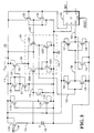
- the input line 13 which as mentioned above is a uniform potential line, is connected to a pad of the integrated circuit at one end and to a gate of a field effect transistor (FET) 112 at its other end.
- FET field effect transistor
- the monitor 10 has the N channel FET (n-FET) 112 as its input detector 12.
- the drain of the n-FET 112 is connected to a more positive conductor grid 113 of the integrated circuit.
- the more positive conductor grid 113 is connected via multiple pins (not independently shown) to voltage +VDD of an external voltage-and-current supply (not shown).
- the voltage +VDD seems as if it is connected to the more positive conductor grid 113 at approximately the center of the integrated circuit. Under low to medium current conditions, the voltage supplied to the more positive grid 113 will remain substantially the same even if the pin or the pad associated with the input line 13 has a faulty connection causing local noise voltages at that point.
- the source of the n-FET 112 is connected via line 114 to a capacitor 116.
- the voltage on line 13 exceeds the gate-to-source threshold voltage of n-FET 112
- the n-FET 112 begins to conduct current from its drain to its source.
- Such an input voltage may be caused by a faulty connection between a connection pad and its respective pin when the device is operating as a current source (secondary or controlled current source), or as a current sink.
- Faulty connections typically have two components: a linear voltage caused by a poorly conducting connection and noise caused by non-linearities of a poor connection. The fault voltages are usually highest in the immediate proximity of the faulty connection but can be spread to the nearby core logic circuits (not shown).
- the drain-to-source current of the input detector FET 112 is conducted via line 114 to the capacitor 116, where it is quickly accumulated in a known way to develop a sample voltage.
- the accumulated current is bled off at a slow rate relative to the accumulation rate via line 115 by n-FET 117C.
- N-FET 117C is biased to electrical function as a resistor.
- P-FET 117A and n-FET 117B form a voltage divider and divide the potential difference between the more positive conductor grid 113 and its counterpart, more negative conductor grid 119.
- n-FET 117C The gate of n-FET 117C is connected to this divided potential and is thereby biased at a constant voltage level, resulting in a constant resistance between the drain and source of n-FET 117C.
- This constant resistance slowly bleeds off the voltage accumulated across the capacitor 116.
- Line 115 connects the more positive plate of the capacitor 116 to voltage comparator 120 which in the preferred embodiment is a differential amplifier formed from FETs 120A, 120B, 120C and 120D.
- P-FETs 120A and 120C are input transistors for the differential amplifier.
- N-FETs 120B and 120D are identical in fabrication, and their gates are connected to a common point. In this configuration, n-FETs 120B and 120D provide equal series load resistances to their respective input p-FETs 120A and 120C.
- P-FET 120A has its gate connected to line 115 in order to receive fault signals from the holding capacitor 116.
- P-FET 120C the other input of the differential amplifier, has its gate connected via line 122 to a mid point of a voltage divider formed by the series connection of n-FETs 123 and 124.
- N-FETs 123 and 124 are connected in series between the more positive conductor grid 113 and the more negative conductor grid 119.
- Their gates are tied to a common point, e.g. +VDD, so the voltage division between these two will depend on the channel resistance of each.
- One embodiment of the invention which has been simulated by a computer simulation program, had selected channel resistances that provided a forty-to-one division of +VDD.
- the differential amplifier compares fault voltage input connected to p-FET 120A with the constant voltage reference of approximately one-fortieth +VDD connected to the other input, p-FET 120C.
- the differential amplifier p-FETs 120A and 120C have their sources tied to a common line 126.
- the common line 126 connects the differential amplifier to a drain of a p-FET 130.
- the source of the p-FET 130 is connected to the more positive conductor grid 113.
- the gate of p-FET 130 is connected to another voltage divider formed by p-FETs 127 and 128.
- the gate and the drain of p-FET 127 are connected to the more negative conductor grid 119.
- the source of p-FET 127 is connected to the gate and drain of p-FET 128, and also to output line 129.
- the source of p-FET 128 is connected to the more positive conductor grid 113 to complete the voltage divider.
- p-FETs 127 and 128 divide the voltage difference between the more negative conductor grid 119 and the more positive conductor grid 113, i.e. +VDD.
- p-FETs 127 and 128 were selected such that the voltage at output line 129 would be approximately 3/5 (+VDD), but other variations of this voltage division ratio of this embodiment are deemed to be within the scope of the present invention.
- Output line 129 connects the divided voltage to the gate of p-FET 130.
- the p-FET 130 with the constant divided voltage on its gate conducts a constant current (within its operating range) to the common branch of the differential amplifier via line 126.
- a constant current device in the common branch allows the common supply voltage +VDD and its return (i.e. circuit ground) to vary without causing changes in the comparison point which is determined by the reference voltage on line 122.
- the differential amplifier 120 which generally performs the function of the voltage comparator 20 in Fig. 1, amplifies as well as compares the difference between the reference voltage on line 122 and the input from the holding capacitor 116.
- a single ended output is taken from the differential amplifier 120 between p-FET 120C and n-FET 120D.
- This single ended output is connected via line 133 to a Schmitt trigger stage formed by p-FETs 134 and 137, and n-FETs 135, 138, and 139.
- the p-FET 134 and the n-FET 135 are connected as a standard complementary symmetry inverter between the more positive grid 113 and the more negative grid 119.
- the complementary symmetry inverter has a constant, high input impedance input, and thus, does not load down the differential stage when line 133 connects the gates of FETs 134 and 135 to the single ended output of the differential amplifier 120.
- the output of FETs 134, 135 is connected via line 136 to the commonly connected gates of a second complementary symmetry inverter formed by p-FET 137 and n-FET 138, which are also connected between the more positive grid 113 and the more negative grid 119.
- the output of this second complementary inverter stage is fed back via conductor 140 to a gate of an n-FET 139.
- the drain of n-FET 139 is connected to line 136 and its source is connected to the more negative grid 119.
- n-FET 139 When the output of the first complementary stage on line 136 is a low voltage, the output of FETs 137, 138 is a high voltage, and n-FET 139 is driven to a low impedance state between its drain and source. This low impedance state pulls the already low level of line 136 lower yet, and accelerates the rate of the level change. The low impedance state of n-FET 139 also increases the amount of current drive required to change the state of FETs 137, 138 back to the high level, thus providing the fast switching characteristic of a Schmitt trigger.
- the output of the first complementary stage is a high voltage
- the output of FETs 137, 138 is a low voltage
- n-FET 139 is driven to a high impedance state between its drain and its source, thereby increasing the amount of current drive available to the gates of FETs 137 and 138 and accelerating the switching time of the change of state.
- the Schmitt trigger stage resists a change of logic state by the feedback action of n-FET 139 until a signal having a sufficient voltage level to trigger FETs 134 and 135 is encountered. Once a state change has reached the trigger threshold, the positive feedback action of the n-FET 139 accelerates the change to drive the complementary inverter stage of FETs 137 and 138 to the next state even faster.
- the Schmitt trigger stage of FETs 134, 135, 137, 138, and 139 shapes its slowly changing input voltage to a quickly transitioning binary signal.
- the output of the Schmitt trigger circuit is connected via line 140 to a flip-flop 141.
- the preferred embodiment of the invention has an edge triggered, clocked S-R flip-flop as the flip-flop 141. This embodiment has the S input connected to the high logic level, the R input is connected to the low logic level, and the clock input connected to the Schmitt trigger output.
- the asynchronous clear input of flip-flop 141 is connected to a special reset circuit that is separate from the normal reset of the integrated circuit. In operation, the flip-flop 141 is asynchronously cleared at the beginning of the monitor period and any subsequent change of the logic level on line 140 will clock a high logic level into flip-flop 141 from the S input. Once a high logic level has been clocked in from the S input, the only way for the state of flip-flop 141 to change is to have its asynchronous reset terminal asserted as it is at the beginning of every monitoring period.
- FIG. 3 another embodiment of the invention is shown.
- the primary difference between the supply connection integrity monitor 10A and the monitor 10 shown in Fig. 2 is that the monitor 10A has a p-FET 112A as its input detector instead of the n-FET 112.
- An input 13A is connected to a more positive pad of an integrated circuit in order to monitor a pin which is connected to the more positive conductor of the voltage and current supply.
- the source and substrate terminals of the p-FET 112A are connected to the more positive conductor grid 113, and the drain of p-FET 112A is connected via line 114 to the capacitor 116.
- the remainder of the monitor circuit 10A is virtually identical in connection and operation to the monitor circuit 10 shown in Fig. 2. It may be desirable to vary the reference voltages of the differential amplifier because of the differences in the voltage reference frame, but as mentioned before, such modifications are deemed to be within the scope of the present invention.
- FIG. 2 operation of the supply integrity monitor 10 will be described.
- the operation of the supply integrity monitor 10A will be very similar except that the operation of the input detector will be slightly different because of the difference in polarity.
- the line 13 is a low current line that connects to a pad (not shown) of a pin that is externally connected to the more negative supply voltage, that is, integrated circuit ground.
- the pad is also connected by a high current conductor (not shown) to the more negative conductor grid 119.
- n-FET 112 and the capacitor 116 are located close to the monitored pad in order to detect and hold any locally occurring noise pulses, which would indicate a faulty condition, such as from pad-to-pin fault or from pin-to-printed wiring board fault. Such locally caused voltage pulses will cause current to flow through the detector 112.
- Capacitor 116 with FETs 117A, 117B, and 117C arranged as a very high resistance bleeder, is almost instantaneously charged by the current from the detector 112.
- Capacitor 116 develops and holds a sample voltage that is essentially the input peak voltage minus the gate-to-source threshold voltage of FET 112.
- the sample voltage held by capacitor 116 is applied to one input of the differential amplifier 120 formed by FETs 120A-120D.
- the other input of the differential amplifier 120 is connected to a constant reference voltage supplied by FETs 123 and 124.
- the differential amplifier 120 amplifies the difference between the average voltage across capacitor 116 and the reference voltage of FETs 123 and 124 and thus operates as a voltage comparator.
- the differential amplifier 120 as a voltage comparator changes state very slowly.
- many digital devices require a relatively rapid change between binary states in order to allow their logic gates a chance to switch quickly to the next binary state.
- the Schmitt trigger with its signal shaping characteristics described previously, shortens the rise time of the slow transitioning output signal from the differential amplifier 120 into a fast rising clock pulse that will reliably clock the flip-flop 141.
- the Schmitt trigger will sharpen the slowly changing output signal from differential amplifier 120 into a fast rise time clock pulse that will reliably clock flip-flop 141 from its initial low state to a high logic level to record the fault.
- the changed state will remain until specially cleared by external circuits.
- the state of flip-flop 141 may be read at any time by external circuitry connected to its non inverted output. Thus, otherwise difficult or undetectable faulty connections of an integrated circuit may be monitored, and the results recorded for later diagnostic and/or maintenance operations.
Landscapes
- Tests Of Electronic Circuits (AREA)
- Testing Of Short-Circuits, Discontinuities, Leakage, Or Incorrect Line Connections (AREA)
- Testing Or Measuring Of Semiconductors Or The Like (AREA)
Claims (7)
- Dispositif de circuit intégré ayant un dispositif de contrôle d'intégrité de la connexion d'alimentation, comprenant un contact de connexion d'alimentation, un détecteur de tension (112) connecté électriquement audit contact de connexion et adapté pour conduire un courant en réponse à une tension d'entrée qui dépasse un premier seuil ; un circuit de maintien (116) connecté audit détecteur de tension (112) et adapté pour délivrer une tension qui est sensiblement égale à ladite tension d'entrée moins ledit premier seuil ; un circuit de tension de référence (122, 123, 124) adapté pour fournir une tension de référence, un comparateur de tension (120) ayant une première entrée connectée audit circuit de maintien (116) et une deuxième entrée connectée audit circuit de tension de référence (122, 123, 124) et adapté pour comparer la tension de sortie dudit circuit de maintien (116) à ladite tension de référence et pour déterminer une tension de sortie de comparateur si la tension de sortie dudit circuit de maintien (116) dépasse ladite tension de référence ; un circuit de déclenchement (134 à 138) dont l'entrée est connectée à la sortie dudit comparateur de tension (120), et adapté pour déclencher sa sortie d'un premier état de sortie à un deuxième état de sortie si la tension de l'entrée de déclenchement dépasse un deuxième seuil ; et un composant mémoire (141) adapté pour stocker un chiffre binaire si la sortie dudit circuit de déclenchement (134 à 138) passe dudit premier état de sortie audit deuxième état de sortie.
- Dispositif de circuit intégré selon la revendication 1, caractérisé en ce que ledit comparateur de tension (120) est un amplificateur différentiel.
- Dispositif de circuit intégré selon la revendication 1 ou la revendication 2, caractérisé par des moyens de polarisation (130) connectés audit comparateur de tension (120) et adaptés pour délivrer une tension de polarisation auxdites première et deuxième entrées dudit comparateur de tension (120).
- Dispositif de circuit intégré selon la revendication 3, caractérisé en ce que lesdits moyens de polarisation sont constitués par un transistor en mode commun (130) dont l'électrode de commande est connectée à des deuxièmes moyens de référence de tension (127, 128).
- Dispositif de circuit intégré selon l'une quelconque des revendications précédentes, caractérisé en ce que ledit composant mémoire est une bascule (141) ayant une entrée de remise à zéro qui remet à zéro seulement ladite bascule (141).
- Dispositif de circuit intégré selon la revendication 5, caractérisé en ce que ladite bascule (141) a une sortie qui peut être accédée par un circuit logique externe audit circuit intégré.
- Procédé de contrôle d'une tension susceptible de provoquer une défaillance au niveau d'un contact sur un circuit intégré selon la revendication 1, comprenant les étapes consistant à : (a) détecter si une tension d'entrée dudit contact dépasse une tension de seuil de manière à produire une tension susceptible de provoquer une défaillance ; (b) maintenir une tension d'échantillon d'amplitude égale à une quantité de laquelle ladite tension d'entrée dépasse ladite tension de seuil ; (c) comparer ladite tension d'échantillon à une tension de référence et produire un signal de sortie de déclenchement qui peut commuter d'un premier état binaire à un deuxième état binaire si ladite tension d'échantillon dépasse ladite tension de référence ; (d) enregistrer la variation de ladite tension de sortie binaire dans un composant mémoire ; et (e) lire une sortie dudit composant mémoire afin de déterminer si la tension susceptible de produire une défaillance s'est produite.
Applications Claiming Priority (2)
| Application Number | Priority Date | Filing Date | Title |
|---|---|---|---|
| US456759 | 1989-12-26 | ||
| US07/456,759 US5077521A (en) | 1989-12-26 | 1989-12-26 | Supply connection integrity monitor |
Publications (3)
| Publication Number | Publication Date |
|---|---|
| EP0436358A2 EP0436358A2 (fr) | 1991-07-10 |
| EP0436358A3 EP0436358A3 (en) | 1992-06-10 |
| EP0436358B1 true EP0436358B1 (fr) | 1997-09-24 |
Family
ID=23814046
Family Applications (1)
| Application Number | Title | Priority Date | Filing Date |
|---|---|---|---|
| EP90313994A Expired - Lifetime EP0436358B1 (fr) | 1989-12-26 | 1990-12-20 | Circuit intégré ayant un moniteur pour l'intégrité des connexions d'alimentation |
Country Status (4)
| Country | Link |
|---|---|
| US (1) | US5077521A (fr) |
| EP (1) | EP0436358B1 (fr) |
| JP (1) | JP2956855B2 (fr) |
| DE (1) | DE69031489T2 (fr) |
Families Citing this family (9)
| Publication number | Priority date | Publication date | Assignee | Title |
|---|---|---|---|---|
| JPH07229932A (ja) * | 1994-02-17 | 1995-08-29 | Toshiba Corp | 電位検知回路 |
| JP2654352B2 (ja) * | 1994-07-29 | 1997-09-17 | 日本電気アイシーマイコンシステム株式会社 | 半導体集積回路 |
| US5550701A (en) * | 1994-08-30 | 1996-08-27 | International Rectifier Corporation | Power MOSFET with overcurrent and over-temperature protection and control circuit decoupled from body diode |
| FR2732133B1 (fr) * | 1995-03-21 | 1997-04-25 | Sgs Thomson Microelectronics | Detecteur de coherence d'informations contenues dans un circuit integre |
| US6134686A (en) * | 1998-05-29 | 2000-10-17 | Cypress Semiconductor Corp. | Technique to detect drive strength of input pin |
| US20030018937A1 (en) * | 2001-07-18 | 2003-01-23 | Athavale Atul S. | Method and apparatus for efficient self-test of voltage and current level testing |
| TWI240243B (en) * | 2003-05-06 | 2005-09-21 | Au Optronics Corp | Liquid crystal display driving circuit and verifying apparatus and error tolerance method thereof |
| US7123039B2 (en) * | 2004-08-13 | 2006-10-17 | Jason Gonzalez | Testing input/output voltages in integrated circuits |
| TWI459186B (zh) * | 2011-11-18 | 2014-11-01 | Inventec Corp | 電壓錯誤的處理裝置與方法 |
Family Cites Families (13)
| Publication number | Priority date | Publication date | Assignee | Title |
|---|---|---|---|---|
| US3590370A (en) * | 1969-04-09 | 1971-06-29 | Leeds & Northrup Co | Method and apparatus for detecting the open-circuit condition of a thermocouple by sending a pulse through the thermocouple and a reactive element in series |
| US3796947A (en) * | 1973-02-27 | 1974-03-12 | Bell Telephone Labor Inc | Electron beam testing of film integrated circuits |
| US3873818A (en) * | 1973-10-29 | 1975-03-25 | Ibm | Electronic tester for testing devices having a high circuit density |
| US4168527A (en) * | 1978-02-17 | 1979-09-18 | Winkler Dean A | Analog and digital circuit tester |
| DE2925483C2 (de) * | 1979-06-23 | 1984-08-23 | Kistler Instrumente Ag, Winterthur | Verfahren und Vorrichtung zum Messen und Auswerten der Spitzenwerte eines pulsierenden Spannungsmessignals |
| US4384350A (en) * | 1980-11-03 | 1983-05-17 | Fairchild Camera & Instrument Corp. | MOS Battery backup controller for microcomputer random access memory |
| JPS58115372A (ja) * | 1981-12-29 | 1983-07-09 | Fujitsu Ltd | 半導体装置試験回路 |
| DE3209562A1 (de) * | 1982-03-16 | 1983-09-29 | Siemens AG, 1000 Berlin und 8000 München | Schaltungsanordnung zur erkennung und speicherung von netzfehlern |
| US4507713A (en) * | 1983-10-11 | 1985-03-26 | Allied Corporation | Wide frequency multi-phase undervoltage detection circuit |
| DE3446958A1 (de) * | 1984-12-21 | 1986-07-10 | Siemens AG, 1000 Berlin und 8000 München | Anordnung zur kurzschluss- bzw. ueberlastueberwachung bei elektronischen naeherungsschaltern |
| US4762663A (en) * | 1986-04-08 | 1988-08-09 | Westinghouse Electric Corp. | Self-testing monitoring circuit |
| JPH0348795Y2 (fr) * | 1986-12-27 | 1991-10-17 | ||
| US4951171A (en) * | 1989-05-11 | 1990-08-21 | Compaq Computer Inc. | Power supply monitoring circuitry for computer system |
-
1989
- 1989-12-26 US US07/456,759 patent/US5077521A/en not_active Expired - Lifetime
-
1990
- 1990-11-30 JP JP2330915A patent/JP2956855B2/ja not_active Expired - Fee Related
- 1990-12-20 DE DE69031489T patent/DE69031489T2/de not_active Expired - Lifetime
- 1990-12-20 EP EP90313994A patent/EP0436358B1/fr not_active Expired - Lifetime
Also Published As
| Publication number | Publication date |
|---|---|
| EP0436358A2 (fr) | 1991-07-10 |
| DE69031489T2 (de) | 1998-04-09 |
| JPH03203250A (ja) | 1991-09-04 |
| DE69031489D1 (de) | 1997-10-30 |
| EP0436358A3 (en) | 1992-06-10 |
| US5077521A (en) | 1991-12-31 |
| JP2956855B2 (ja) | 1999-10-04 |
Similar Documents
| Publication | Publication Date | Title |
|---|---|---|
| JP3088727B2 (ja) | 零入力電流測定装置 | |
| US4336495A (en) | Integrated circuit arrangement in MOS-technology with field-effect transistors | |
| US6954079B2 (en) | Interface circuit coupling semiconductor test apparatus with tested semiconductor device | |
| US3795859A (en) | Method and apparatus for determining the electrical characteristics of a memory cell having field effect transistors | |
| US4630270A (en) | Method for identifying a faulty cell in a chain of cells forming a shift register | |
| US6031386A (en) | Apparatus and method for defect testing of integrated circuits | |
| US5077521A (en) | Supply connection integrity monitor | |
| KR100190215B1 (ko) | 반도체 집적 회로 | |
| US6262585B1 (en) | Apparatus for I/O leakage self-test in an integrated circuit | |
| WO2001023902A1 (fr) | Perfectionnements apportes a des dispositifs de test equipant des cartes de deverminage | |
| EP3474027B1 (fr) | Procédé d'identification d'un défaut à la sortie d'un dispositif et système correspondant | |
| US4743842A (en) | Tri-state circuit tester | |
| US5672982A (en) | Semiconductor integrated circuit | |
| US5343479A (en) | Semiconductor integrated circuit having therein circuit for detecting abnormality of logical levels outputted from input buffers | |
| EP3477317B1 (fr) | Procédé d'identification d'un défaut à la sortie d'un dispositif et système correspondant | |
| US5796260A (en) | Parametric test circuit | |
| EP0338220B1 (fr) | Circuits logiques du type multiplexeur | |
| US5826004A (en) | Input/output device with self-test capability in an integrated circuit | |
| US5912562A (en) | Quiescent current monitor circuit for wafer level integrated circuit testing | |
| US5705944A (en) | Method and device for detecting internal resistance voltage drop on a chip | |
| US5068599A (en) | Integrated circuit having an enabling circuit for controlling primary and secondary subcircuits | |
| EP0190427B1 (fr) | Système pour détecter des erreurs logiques stochastiques pour réseaux logiques différentiels | |
| JPH11326441A (ja) | 半導体試験装置 | |
| US5570036A (en) | CMOS buffer circuit having power-down feature | |
| EP1977261B1 (fr) | Dispositif d'evaluation de retard d'un circuit d'entree/sortie |
Legal Events
| Date | Code | Title | Description |
|---|---|---|---|
| PUAI | Public reference made under article 153(3) epc to a published international application that has entered the european phase |
Free format text: ORIGINAL CODE: 0009012 |
|
| AK | Designated contracting states |
Kind code of ref document: A2 Designated state(s): DE FR GB NL |
|
| PUAL | Search report despatched |
Free format text: ORIGINAL CODE: 0009013 |
|
| AK | Designated contracting states |
Kind code of ref document: A3 Designated state(s): DE FR GB NL |
|
| 17P | Request for examination filed |
Effective date: 19921117 |
|
| RAP1 | Party data changed (applicant data changed or rights of an application transferred) |
Owner name: NCR INTERNATIONAL INC. |
|
| RAP1 | Party data changed (applicant data changed or rights of an application transferred) |
Owner name: AT&T GLOBAL INFORMATION SOLUTIONS INTERNATIONAL IN |
|
| RAP1 | Party data changed (applicant data changed or rights of an application transferred) |
Owner name: AT&T GLOBAL INFORMATION SOLUTIONS INTERNATIONAL IN Owner name: HYUNDAI ELECTRONICS AMERICA |
|
| 17Q | First examination report despatched |
Effective date: 19950504 |
|
| RAP1 | Party data changed (applicant data changed or rights of an application transferred) |
Owner name: HYUNDAI ELECTRONICS AMERICA Owner name: AT&T GLOBAL INFORMATION SOLUTIONS INTERNATIONAL IN Owner name: SYMBIOS LOGIC INC. |
|
| GRAG | Despatch of communication of intention to grant |
Free format text: ORIGINAL CODE: EPIDOS AGRA |
|
| RAP1 | Party data changed (applicant data changed or rights of an application transferred) |
Owner name: SYMBIOS LOGIC INC. Owner name: NCR INTERNATIONAL, INC. Owner name: HYUNDAI ELECTRONICS AMERICA |
|
| GRAH | Despatch of communication of intention to grant a patent |
Free format text: ORIGINAL CODE: EPIDOS IGRA |
|
| GRAH | Despatch of communication of intention to grant a patent |
Free format text: ORIGINAL CODE: EPIDOS IGRA |
|
| GRAA | (expected) grant |
Free format text: ORIGINAL CODE: 0009210 |
|
| AK | Designated contracting states |
Kind code of ref document: B1 Designated state(s): DE FR GB NL |
|
| REF | Corresponds to: |
Ref document number: 69031489 Country of ref document: DE Date of ref document: 19971030 |
|
| ET | Fr: translation filed | ||
| NLT1 | Nl: modifications of names registered in virtue of documents presented to the patent office pursuant to art. 16 a, paragraph 1 |
Owner name: NCR INTERNATIONAL, INC;HYUNDAI ELECTRONICS AMERICA |
|
| PLBE | No opposition filed within time limit |
Free format text: ORIGINAL CODE: 0009261 |
|
| STAA | Information on the status of an ep patent application or granted ep patent |
Free format text: STATUS: NO OPPOSITION FILED WITHIN TIME LIMIT |
|
| 26N | No opposition filed | ||
| REG | Reference to a national code |
Ref country code: GB Ref legal event code: IF02 |
|
| NLS | Nl: assignments of ep-patents |
Owner name: HYNIX SEMICONDUCTOR INC. Owner name: HYUNDAI ELECTRONICS AMERICA Owner name: NCR INTERNATIONAL, INC |
|
| NLT1 | Nl: modifications of names registered in virtue of documents presented to the patent office pursuant to art. 16 a, paragraph 1 |
Owner name: NCR INTERNATIONAL, INC Owner name: HYNIX SEMICONDUCTOR AMERICA INC. |
|
| REG | Reference to a national code |
Ref country code: GB Ref legal event code: 732E |
|
| REG | Reference to a national code |
Ref country code: FR Ref legal event code: TP |
|
| NLS | Nl: assignments of ep-patents |
Owner name: MAGNACHIP SEMICONDUCTOR LTD. Effective date: 20060913 Owner name: NCR INTERNATIONAL, INC Effective date: 20060913 |
|
| REG | Reference to a national code |
Ref country code: GB Ref legal event code: 732E |
|
| REG | Reference to a national code |
Ref country code: GB Ref legal event code: 732E |
|
| REG | Reference to a national code |
Ref country code: FR Ref legal event code: TQ |
|
| PGFP | Annual fee paid to national office [announced via postgrant information from national office to epo] |
Ref country code: NL Payment date: 20091224 Year of fee payment: 20 |
|
| PGFP | Annual fee paid to national office [announced via postgrant information from national office to epo] |
Ref country code: GB Payment date: 20091229 Year of fee payment: 20 Ref country code: FR Payment date: 20100106 Year of fee payment: 20 |
|
| PGFP | Annual fee paid to national office [announced via postgrant information from national office to epo] |
Ref country code: DE Payment date: 20091230 Year of fee payment: 20 |
|
| REG | Reference to a national code |
Ref country code: NL Ref legal event code: V4 Effective date: 20101220 |
|
| REG | Reference to a national code |
Ref country code: GB Ref legal event code: PE20 Expiry date: 20101219 |
|
| PG25 | Lapsed in a contracting state [announced via postgrant information from national office to epo] |
Ref country code: NL Free format text: LAPSE BECAUSE OF EXPIRATION OF PROTECTION Effective date: 20101220 Ref country code: GB Free format text: LAPSE BECAUSE OF EXPIRATION OF PROTECTION Effective date: 20101219 |
|
| PG25 | Lapsed in a contracting state [announced via postgrant information from national office to epo] |
Ref country code: DE Free format text: LAPSE BECAUSE OF EXPIRATION OF PROTECTION Effective date: 20101220 |