EP0436603B1 - Procede et dispositif pour convertir le signal de balayage d'un signal d'entree analogique - Google Patents
Procede et dispositif pour convertir le signal de balayage d'un signal d'entree analogique Download PDFInfo
- Publication number
- EP0436603B1 EP0436603B1 EP89910865A EP89910865A EP0436603B1 EP 0436603 B1 EP0436603 B1 EP 0436603B1 EP 89910865 A EP89910865 A EP 89910865A EP 89910865 A EP89910865 A EP 89910865A EP 0436603 B1 EP0436603 B1 EP 0436603B1
- Authority
- EP
- European Patent Office
- Prior art keywords
- value
- digital
- partial
- analogue
- signal
- Prior art date
- Legal status (The legal status is an assumption and is not a legal conclusion. Google has not performed a legal analysis and makes no representation as to the accuracy of the status listed.)
- Expired - Lifetime
Links
Images
Classifications
-
- H—ELECTRICITY
- H03—ELECTRONIC CIRCUITRY
- H03M—CODING; DECODING; CODE CONVERSION IN GENERAL
- H03M1/00—Analogue/digital conversion; Digital/analogue conversion
- H03M1/12—Analogue/digital converters
- H03M1/18—Automatic control for modifying the range of signals the converter can handle, e.g. gain ranging
- H03M1/181—Automatic control for modifying the range of signals the converter can handle, e.g. gain ranging in feedback mode, i.e. by determining the range to be selected from one or more previous digital output values
-
- H—ELECTRICITY
- H03—ELECTRONIC CIRCUITRY
- H03M—CODING; DECODING; CODE CONVERSION IN GENERAL
- H03M1/00—Analogue/digital conversion; Digital/analogue conversion
- H03M1/12—Analogue/digital converters
- H03M1/14—Conversion in steps with each step involving the same or a different conversion means and delivering more than one bit
- H03M1/16—Conversion in steps with each step involving the same or a different conversion means and delivering more than one bit with scale factor modification, i.e. by changing the amplification between the steps
- H03M1/164—Conversion in steps with each step involving the same or a different conversion means and delivering more than one bit with scale factor modification, i.e. by changing the amplification between the steps the steps being performed sequentially in series-connected stages
-
- H—ELECTRICITY
- H03—ELECTRONIC CIRCUITRY
- H03M—CODING; DECODING; CODE CONVERSION IN GENERAL
- H03M1/00—Analogue/digital conversion; Digital/analogue conversion
- H03M1/12—Analogue/digital converters
- H03M1/34—Analogue value compared with reference values
- H03M1/36—Analogue value compared with reference values simultaneously only, i.e. parallel type
- H03M1/361—Analogue value compared with reference values simultaneously only, i.e. parallel type having a separate comparator and reference value for each quantisation level, i.e. full flash converter type
Definitions
- the invention relates to a method for converting the scanning signal of an analog input signal into a digital output value to L data bits, the scanning signal being converted into a digital reference value to M ⁇ L data bits, which in turn is converted back into an analog reference signal and subtracted from the scanning signal, the latter Differential signal amplified and converted into a digital partial value to M ⁇ N ⁇ L data bits, which is combined with the reference value for the output value with L data bits, the higher value data bits and the lower value data bits of the output value being formed from the reference value and the sum of the number of Data bits of reference and partial value are not less than the number of data bits of the output value.
- DE-A-2 026 643 discloses an analog / digital converter according to the subrange method, in which a first digital partial result is first obtained from an electrical analog input variable in a relatively low accuracy analog / digital converter (Reference value) is formed and saved. This partial result is converted back to the full, desired accuracy in a digital / analog converter and the difference is formed from this with the input variable. Finally, after amplifying this difference variable, a second digital partial result is obtained, which is combined in a result register with the first partial result to form the initial value.
- a similar analog / digital converter is also described in DE-A-1 801 670.
- the invention has for its object to avoid interference in the formation of the difference signal.
- the reference value is only formed during a sampling period as part of a working cycle and is held until the next following sampling period and that the subtraction of the reference signal is suppressed when the level of the sampling signal drops below the minimum quantization level for reference value formation.
- the information contained in the difference signal from the range of small input signal levels is converted with high resolution and good linearity. Furthermore, since the partial value is shifted downward when the initial value is formed, all errors in the partial value formation are reduced in relation to the initial value. Voltage peaks in the formation of the difference signal due to transit time differences between the scanning signal and the reference signal are reduced to a non-disturbing level by the division of the working cycle. Furthermore, this operating mode eliminates the need for a latch at the converter output. The difference between the reference and the sampling signal may only be so great that the downstream amplifier does not fall into the saturation range.
- the sum of the data bits of the reference and partial value is not significantly greater than the number of data bits of the output value and that the excess data bits are used to correct conversion errors and to indicate that the value range has been exceeded.
- the overlap of the reference with the partial value makes it possible to eliminate the errors in the reference value formation with the most significant bit of the partial value.
- the invention further relates to a method for converting a digital input value into an analog output signal, the digital input value being split into two partial values and being converted into analog partial signals, the more significant bits of the input value forming the upper partial value and, at the same time, with the less significant bits into analog partial signals are converted, the number of the higher order bits being smaller than the number of the lower order bits, and the partial signals with level adjustment being summed and combined to form the output signal.
- the digital / analog converter operates in accordance with Electronic Engineering, Volume 57, No. 704, August 1985, (London, GB), L.M. Radhakrishnan: "Two 8 bit DAC's make a 12 bit DAC", page 30.
- the level is only adjusted via a resistor. Audible errors can occur when using low-resolution components.
- the object of the invention is also to avoid disturbances in the formation of the sum signal.
- a device for analog / digital conversion can be produced with generally available components, the input signal being fed to a sample and hold element, the output of which is connected to the analog input of an M-bit parallel A / D converter, the outputs of the parallel A / D converter are connected to the digital inputs of a reference D / A converter and the higher-value inputs of an L-bit bistable latch, the output of the reference D / A converter being connected to the output of the sample and hold element in a differential amplifier is merged, the output of which is connected to the analog input of an N-bit partial value A / D converter and the outputs of the partial value A / D converter are connected to the lower-order inputs of the latch and inputs of a correction circuit to the outputs of the parallel A / D converter are connected, which is characterized for performing an error correction in that a further input of the correction circuit m It is connected to the most significant output of the partial value A / D converter that the outputs of the correction circuit are connected to the higher-order inputs of the latch, an
- a data bus for input values is connected to a low-value and an upper-value D / A converter, the outputs of which are combined in a summing amplifier, that a noise suppression circuit between the upper-value D / A converter and the summing amplifier is arranged that the noise suppression circuit for adding a digital fixed value is connected via a gate to the most significant lines of the data bus and that a transmission memory is connected in series with a recording memory.
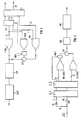
- Fig. 1 is the block diagram of a 20-bit analog / digital converter assembly of a sound channel of a digital studio mixer shown with linear converter characteristic.
- An analog audio signal is present at the input of an AAF echo filter, which limits the audio frequency to a maximum of 20 kHz. This suppresses higher frequencies that could become audible after the conversion.
- a sample-and-hold element SH with 48 kHz generates a pulse-amplitude-modulated sample signal with discrete DC voltage, which is converted into a digital output value in two parallel steps.
- a fast 5-bit parallel A / D converter FAD generates a digital 5-bit approximate value of the scanning signal.
- this reference value is fed to a latch L as part of the output value
- the most significant bits of a 16-bit reference D / A converter RDA are converted back into an analog reference signal and subtracted from the scanning signal with a differential amplifier DV.
- This difference signal is amplified by a factor of 16 and fed to a 16-bit partial value A / D converter AD.
- the now most significant bit of the partial value is fed to a correction circuit KS and used as a digital superimposition value for correcting errors in the reference value formation of the parallel A / D converter FAD.
- the reference value is combined as a higher-value part and the remaining 15 bits of the partial value as a lower-value part of the output value.
- the gain factor of the differential amplifier is DV 32.
- the signal level at the input of the partial value A / D converter AD is always 30 dB higher than at the input of the entire module.
- the partial value is then shifted down by 30 dB. This reduces all errors of the partial value A / D converter AD that occur during the conversion by 30 dB. That gives a very good 20 bit Linearity of the output value, the level of which is more than 30 dB below the maximum value. This area is particularly important for audio signals, since errors would be easily audible.
- the only limitation on the overall accuracy of the analog / digital conversion for scanning signals above the minimum quantization level of the parallel A / D converter FAD is the accuracy of the reference D / A converter RDA when using the correction circuit KS.
- the AAF echo filter consists of an operational amplifier (1/2 NE 5532), a 4th order Butterworth low-pass filter and a 1st order passive filter. This reduces the broadband noise and the phase dispersion of the filters.
- the isolation between the sample signal and the holding capacitors is improved by two dual field effect transistors (2x N 5911). Discharge of the holding capacitors is prevented by integration with an operational amplifier (LF 356).
- the parallel A / D converter FAD is unipolar and of the MP 7682 type. It has a resolution of 6 bits and is switched to 5 bits. The output voltage of the sample and hold element SH is adjusted accordingly via resistors.
- the parallel A / D converter FAD is operated in a partial mode. It is clocked at 3.072 MHz only in the sampling period of the sample and hold element SH during a working cycle and remains in the standby position until the next sampling period. The last value at the converter output is held until the next clock pulse sequence.
- a 14-bit converter (ADG 7538) is used as the reference D / A converter RDA and connected in such a way that it works as a 5-bit converter.
- This converter essentially determines the accuracy of the output value of the entire assembly.
- the current output is used instead of the voltage output and the voltage signal is generated by two low-noise operational amplifiers.
- the 5 output bits of the parallel A / D converter FAD become the 5 most significant Inputs of the reference D / A converter RDA fed.
- a first noise suppression circuit NG1 consisting of a field effect transistor (J 110) and a resistor (200 ohms), is connected as a voltage divider to the reference D / A converter RDA.
- a valid value at the output of the parallel A / D converter FAD causes the field effect transistor to be switched off, and the output of the reference D / A converter RDA is connected to the differential amplifier DV.
- the differential amplifier DV consists of an operational amplifier (NE 5534), which is operated inverting on virtual earth.
- the nominal voltage amplification factor is 4.
- the sampling signal at the output of the sample and hold element SH is mixed with the inverted reference signal.
- the partial value is formed from this difference signal by the partial value A / D converter AD.
- a delay between the scanning signal and the reference signal at the input of the differential amplifier DV can generate voltage peaks. Particularly with high-frequency audio signals, there would be strong harmonic distortions.
- the output of the differential amplifier DV could be switched off by an analog switch until the differential signal is stable.
- an additional operational amplifier would be necessary to adapt this analog switch to the partial value A / D converter AD.
- the runtime differences and the voltage peaks resulting therefrom are reduced to a level which is no longer disruptive by operating the reference D / A converter RDA in partial mode. Voltage peaks only occur when the sampling signal is above the minimum quantization level of the parallel A / D converter FAD. Otherwise, as already described, the output of the reference D / A converter RDA is switched off by the first noise reduction circuit NG1.
- the partial value A / D converter AD forms the lower-order bits of the digitized audio signal from the difference signal.
- a 16-bit converter (PCM 75) is used. In the remaining period of a work cycle of 13 ⁇ sec, the difference signal is converted into the partial value.
- the voltage range at the input of the partial value A / D converter AD for the differential signal is set to a quarter of the voltage range of the audio signal. This corresponds to a gain factor 4. Together with the gain factor 4 of the operational amplifier in the differential amplifier DV, the total gain factor of 16, or 24 dB, is achieved in the analog range.
- MSB 16th bit
- the next least significant bit is bit 6 of the 20-bit output value at the latch L.
- the main task of the correction circuit KS is to add the most significant bit of the partial value A / D converter AD to the least significant bit of the parallel A / D converter FAD.
- This correction bit contains all errors that could occur during the parallel conversion of the scanning signal.
- a binary adder 74LS283
- the output signal would have to be digitally limited in order to prevent the value range from being exceeded.
- A27S29 programmable read-only memory
- the addition result is checked for value overflow and, if necessary, reduced to the maximum value (hex3F).
- an overload value is then generated.
- the output value is inverted into the format of the complement of two's complement. If the output of the parallel A / D converter FAD indicates that the minimum quantization level has fallen below (hex1F), the first noise reduction circuit NG1 is activated via the correction circuit KS.
- Fig. 2 shows the digital / analog converter module, which converts a 20-bit input value into an analog audio signal.
- the input value is taken over from a data bus DB into a recording memory L1 and forwarded to a transmission memory L2. This guarantees simultaneous data conversion even with multi-channel systems.
- Recording and transmission memories L1, L2 are made up of D flip-flops (3x 74LS374 each).
- the eight higher-order bits are transferred inverted from the transfer memory L2 as an approximation of the input value to an upper-order D / A converter MS-DAC.
- the twelve least significant bits are fed directly to a low-value D / A converter LS-DAC.
- Low-cost converters are used as low-value and high-value D / A converters LS-DAC, MS-DAC. This enables a powerful, linear 20-bit digital / analog converter module with an operating frequency of up to four times the sampling rate of 48 kHz to be built.
- the levels must be adjusted so that the value of the most significant bit of the low-value D / A converter LS-DAC is half of the value of the least significant bit of the upper value D / A converter MS-DAC. This means that the partial signal at the output of the low-value D / A converter LS-DAC must be attenuated by 48 dB.
- low-noise operational amplifiers are used for current-voltage conversion.
- a second amplifier stage with an inverting operational amplifier on virtual earth raises the output voltage of the upper value D / A converter MS-DAC by 19.2 dB in a summing amplifier SV and by 4 in the low value D / A converter LS-DAC. 8 dB reduced.
- the exact level adjustment of the two partial signals is thus completed.
- the summation takes place in a low-noise operational amplifier (NE 5532) with a gain factor of 2.5 dB.
- a second noise reduction circuit NG2 is used to eliminate this source of error.
- a digital fixed value (digital offset), which corresponds to a direct current, is added to the input value upstream of the recording memory L1, as a result of which the voltage zero crossing of the converter is not connected to a change in polarity of the input value. Interferences that arise when all 20 bits are flipped over at the same time are avoided. The zero crossing is raised significantly for the processing of the audio signals (hex355).
- the digital fixed value also lowers the noise level generated by the digital / analog conversion in the converter.
- a NAND gate G with eight inputs (74LS30) is connected to the eight bits of the partial value of the upper value D / A converter MS-DAC.
- This gate G controls the second noise suppression circuit NG2, which is constructed as a voltage divider from a resistor (390 ohms) and a field effect transistor (J 110).
- the field effect transistor is switched on via gate G and the output of the upper value D / A converter MS-DAC is attenuated by approximately 30 dB.
- the conversion takes place only via the low-value D / A converter LS-DAC, whose output is always attenuated by 24 dB. Its noise level is therefore not a problem.
- the second noise reduction circuit NG2 makes the dynamic range of the entire digital / analog converter module greater than 122 dB.
- the partial value at the input of the upper value D / A converter MS-DAC is inverted. For performance To obtain the module even at higher signal levels, only components with small temperature coefficients should be used.
- the output signal is fed to a smoothing filter DG for removing voltage peaks.
- the level of the output signal can optionally be adjusted by an inverting operational amplifier.
- This circuit uses relatively cheap 16-bit converters and the other common and therefore easily available components to put together a 20-bit converter that delivers very good results for audio purposes. It is also suitable for over-sampling.
Landscapes
- Engineering & Computer Science (AREA)
- Theoretical Computer Science (AREA)
- Analogue/Digital Conversion (AREA)
Abstract
Claims (5)
- Procédé pour la conversion du signal de balayage d'un signal d'entrée analogique en une valeur de sortie numérique en L bits de données, ledit signal de balayage étant converti en une valeur de référence numérique de M < L bits de données, valeur qui est à son tour reconvertie en un signal de référence analogique et soustrait du signal de balayage, tandis que ce signal de différence amplifié est converti en une valeur numérique partielle de M < N < L bits de données laquelle est fusionnée à la valeur de référence pour donner la valeur de sortie de L bits de données, avec formation des bits de poids fort de la valeur de référence et des bits de poids faible de la valeur partielle, de la valeur de sortie, la somme des nombre des bits de données des valeurs de référence et partielle n'étant pas inférieure au nombre des bits de données de la valeur de sortie, caractérisé en ce que la valeur de référence n'est formée que pendant une période de balayage qui représente une partie du cycle opérationnel et qui est maintenue jusqu'à la période de balayage suivante, et en ce que la soustraction du signal de référence est supprimée si le niveau du signal de balayage s'abaisse au-dessous du seuil minimal de quantification pour la formation de la valeur de référence.
- Procédé selon la revendication 1, caractérisé en ce que la somme des bits de données de la valeur de référence et de la valeur partielle n'est pas sensiblement supérieure au nombre de bits de données de la valeur de sortie et en ce que les bits de données en surnombre sont utilisés pour la correction des erreurs de conversion et pour l'affichage d'un dépassement de la plage des valeurs.
- Procédé pour la conversion d'une valeur d'entrée numérique en une valeur de sortie analogique, la valeur d'entrée numérique étant fractionnée en deux valeurs partielles et convertie en des signaux partiels analogiques, alors que les bits de poids fort de la valeur d'entrée constituent la valeur partielle supérieure et sont convertis en même temps que les bits à poids faible en signaux partiels analogiques et que le nombre des bits à poids fort est inférieur à celui des bits à poids faible, les signaux partiels étant additionnés avec ajustement du niveau et fusionnés pour délivrer le signal de sortie, caractérisé en ce que, pour l'ajustement du niveau, dans une première étape, la valeur partielle inférieure est décalée de plusieurs bits vers des positions de poids plus faible et, dans une deuxième étape, le signal partiel inférieur est amorti de la différence de niveau encore présente et en ce qu'une valeur fixe numérique est additionnée à la valeur d'entrée, le signal partiel de la valeur partielle supérieure étant amorti dans une proportion correspondante si les valeurs d'entrée sont inférieures à cette valeur fixe numérique.
- Dispositif pour la mise en oeuvre du procédé de conversion analogique/numérique (figure 1) selon la revendication 1 ou 2, le signal d'entrée étant amené vers un organe de balayage (SH) dont la sortie est reliée à l'entrée analogique d'un convertisseur parallèle A/D (FAD) de M-bit tandis que les sorties de ce convertisseur (FAD) sont reliées aux entrées numériques d'un convertisseur D/A de référence (RDA) et aux entrées de poids fort d'une mémoire bistable de L bit (L), la sortie du convertisseur de référence (RDA) étant fusionnée à la sortie de l'organe de balayage (SH) dans un amplificateur différentiel (DV) dont la sortie est reliée à l'entrée analogique d'un convertisseur de valeur partielle A/D de N-bit (AD) et les sorties de ce convertisseur (AD) étant reliées aux entrées à poids faible de la mémoire (L), alors que des entrées d'un circuit de correction (KS) sont reliées aux sorties du convertissseur (FAD), caractérisé en ce qu'une autre entrée du circuit de correction (KS) est reliée à la sortie de poids fort du convertisseur AD, en ce que des sorties du circuit de correction (KS) sont reliées aux entrées de poids fort de la mémoire (L), qu'une sortie de surcharge du circuit (KS) est reliée à une autre entrée de la mémoire (L) et qu'une sortie de pilotage du circuit (KS) est reliée à un circuit anti-bruit (NG1) et en ce que ce circuit anti-bruit (NG1) est monté, pour la suppression du signal de référence si le niveau du signal de balayage se situe au-dessus du seuil de quantification minimal pour la formation de la valeur de référence, entre le convertisseur (RDA) et l'amplificateur différentiel (DV).
- Dispositif selon la revendication 3 (figure 2), dans lequel un bus de données (DB) pour des valeurs d'entrée est relié à un convertisseur D/A à poids faible et à poids fort (LS-DAC, MS-DAC) dont les sorties sont fusionnées dans un amplificateur sommateur (SV), caractérisé en ce qu'un circuit anti-bruit (NG2) est disposé entre le convertisseur (MS-DAC) et l'amplificateur sommateur (SV), en ce que ce circuit anti-bruit (NG2) est relié à des conduites de poids fort du bus de données (DB) pour l'addition d'une valeur fixe numérique, par une grille (G), et en ce qu'une mémoire de transmission (L2) est montée en série avec une mémoire d'enregistrement (L1).
Applications Claiming Priority (3)
| Application Number | Priority Date | Filing Date | Title |
|---|---|---|---|
| EP88309066 | 1988-09-29 | ||
| EP88309066A EP0360936A1 (fr) | 1988-09-29 | 1988-09-29 | Méthode de conversion d'un signal analogique d'entrée échantillonné |
| PCT/EP1989/001127 WO1990003695A2 (fr) | 1988-09-29 | 1989-09-26 | Procede et dispositif pour convertir le signal de balayage d'un signal d'entree analogique |
Publications (2)
| Publication Number | Publication Date |
|---|---|
| EP0436603A1 EP0436603A1 (fr) | 1991-07-17 |
| EP0436603B1 true EP0436603B1 (fr) | 1994-04-13 |
Family
ID=8200230
Family Applications (2)
| Application Number | Title | Priority Date | Filing Date |
|---|---|---|---|
| EP88309066A Withdrawn EP0360936A1 (fr) | 1988-09-29 | 1988-09-29 | Méthode de conversion d'un signal analogique d'entrée échantillonné |
| EP89910865A Expired - Lifetime EP0436603B1 (fr) | 1988-09-29 | 1989-09-26 | Procede et dispositif pour convertir le signal de balayage d'un signal d'entree analogique |
Family Applications Before (1)
| Application Number | Title | Priority Date | Filing Date |
|---|---|---|---|
| EP88309066A Withdrawn EP0360936A1 (fr) | 1988-09-29 | 1988-09-29 | Méthode de conversion d'un signal analogique d'entrée échantillonné |
Country Status (4)
| Country | Link |
|---|---|
| US (1) | US5148169A (fr) |
| EP (2) | EP0360936A1 (fr) |
| DE (1) | DE58907474D1 (fr) |
| WO (1) | WO1990003695A2 (fr) |
Families Citing this family (4)
| Publication number | Priority date | Publication date | Assignee | Title |
|---|---|---|---|---|
| EP0901058A1 (fr) * | 1991-10-30 | 1999-03-10 | Harris Corporation | Miroir de courant à deux étages |
| US7492297B2 (en) * | 2006-08-11 | 2009-02-17 | Realtek Semiconductor Corp. | Digital-to-analog converter and method thereof |
| US7545295B2 (en) * | 2007-09-14 | 2009-06-09 | Realtek Semiconductor Corp. | Self-calibrating digital-to-analog converter and method thereof |
| WO2016118674A1 (fr) * | 2015-01-22 | 2016-07-28 | La Grou John Howard | Convertisseur numérique-analogique à sommation passive, commuté en série et à trajets multiples |
Citations (4)
| Publication number | Priority date | Publication date | Assignee | Title |
|---|---|---|---|---|
| DE1801670A1 (de) * | 1967-05-16 | 1971-03-04 | Singer General Precision | Vorrichtung zum Umsetzen analoger Signale in digitale Werte |
| DE2026643A1 (de) * | 1970-06-01 | 1971-12-09 | Licentia Gmbh | Anordnung zur Analog-Digital-Umsetzung |
| US4544917A (en) * | 1982-09-16 | 1985-10-01 | Westinghouse Electric Corp. | A/D converter having digitally controlled subranging and self-alignment apparatus for use therein |
| GB2179812A (en) * | 1985-08-23 | 1987-03-11 | Burr Brown Corp | Subranging analog-to-digital converter |
Family Cites Families (12)
| Publication number | Priority date | Publication date | Assignee | Title |
|---|---|---|---|---|
| DE958197C (de) * | 1952-04-18 | 1957-02-14 | Dr Siegfried Skraup | Verfahren zur Herstellung von 2, 4-Diaminochinazolin |
| GB806772A (en) * | 1956-03-29 | 1958-12-31 | Wellcome Found | Diaminoquinazolines and method of preparing |
| CH457460A (fr) * | 1966-06-20 | 1968-06-15 | Parke Davis & Co | Procédé de préparation de quinazolines |
| US3635979A (en) * | 1969-09-29 | 1972-01-18 | Pfizer | Certain 6- and/or 7-alkoxy-substituted-2 4-bis(disubstituted amino) quinazolines |
| US3710377A (en) * | 1971-01-11 | 1973-01-09 | Westinghouse Electric Corp | High speed an analog-to-digital converter |
| GB1390014A (en) * | 1971-05-07 | 1975-04-09 | Koninklijke Pharma Fab Nv | Process for the preparation of carbocyclic fused pyrimidine derivatives |
| US3956495A (en) * | 1973-10-30 | 1976-05-11 | Eli Lilly And Company | 2,4-Diaminoquinazolines as antithrombotic agents |
| JPS6058629B2 (ja) * | 1976-09-27 | 1985-12-20 | ソニー株式会社 | 映像信号のアナログ−デジタル変換回路 |
| US4098788A (en) * | 1977-06-20 | 1978-07-04 | Bristol-Myers Company | Process for preparing quinazolines |
| US4287341A (en) * | 1979-11-01 | 1981-09-01 | Pfizer Inc. | Alkoxy-substituted-6-chloro-quinazoline-2,4-diones |
| JP2690905B2 (ja) * | 1987-08-28 | 1997-12-17 | 株式会社日立製作所 | 直並列形ad変換器 |
| JPS6467034A (en) * | 1987-09-08 | 1989-03-13 | Toshiba Corp | Serial-parallel type a/d converting device |
-
1988
- 1988-09-29 EP EP88309066A patent/EP0360936A1/fr not_active Withdrawn
-
1989
- 1989-09-26 EP EP89910865A patent/EP0436603B1/fr not_active Expired - Lifetime
- 1989-09-26 WO PCT/EP1989/001127 patent/WO1990003695A2/fr not_active Ceased
- 1989-09-26 DE DE58907474T patent/DE58907474D1/de not_active Expired - Fee Related
-
1991
- 1991-05-20 US US07/663,844 patent/US5148169A/en not_active Expired - Fee Related
Patent Citations (4)
| Publication number | Priority date | Publication date | Assignee | Title |
|---|---|---|---|---|
| DE1801670A1 (de) * | 1967-05-16 | 1971-03-04 | Singer General Precision | Vorrichtung zum Umsetzen analoger Signale in digitale Werte |
| DE2026643A1 (de) * | 1970-06-01 | 1971-12-09 | Licentia Gmbh | Anordnung zur Analog-Digital-Umsetzung |
| US4544917A (en) * | 1982-09-16 | 1985-10-01 | Westinghouse Electric Corp. | A/D converter having digitally controlled subranging and self-alignment apparatus for use therein |
| GB2179812A (en) * | 1985-08-23 | 1987-03-11 | Burr Brown Corp | Subranging analog-to-digital converter |
Also Published As
| Publication number | Publication date |
|---|---|
| US5148169A (en) | 1992-09-15 |
| EP0436603A1 (fr) | 1991-07-17 |
| DE58907474D1 (de) | 1994-05-19 |
| WO1990003695A2 (fr) | 1990-04-05 |
| EP0360936A1 (fr) | 1990-04-04 |
| WO1990003695A3 (fr) | 1990-09-07 |
Similar Documents
| Publication | Publication Date | Title |
|---|---|---|
| DE69117794T2 (de) | Mehrstufiger sigma-delta-Analog-zu-Digitalkonverter | |
| DE4237082C2 (de) | Digital/Analog-Konverter mit integriertem Kalibriersystem und Kalibrierverfahren | |
| DE69008360T2 (de) | Paralleler ad-wandler mit 2n-1-vergleichern. | |
| DE69928934T2 (de) | Verfahren und gerät zur korrektur des gleichspannungsversatzes in digital-analog-wandlern | |
| EP1130782B1 (fr) | Procédé et circuit de conversion analogique-numérique de signaux | |
| EP0707383B1 (fr) | Circuit pour conversion de signaux d'anlogiques numériques | |
| DE60029558T2 (de) | Verfahren zum Kalibrieren eines Analog-Digital-Wandlers und eine Kalibrierungsvorrichtung | |
| DE10021824C2 (de) | D/A-Wandlervorrichtung und D/A-Wandlerverfahren | |
| DE69015373T2 (de) | Digital-analog-wandler mit grossem dynamikbereich, hoher genauigkeit und hoher geschwindigkeit. | |
| DE69517411T2 (de) | Effiziente architektur zur korrektur von komponentenfehlanpassungen und schaltungsnichtlinearitäten in a/d umsetzern | |
| DE3021012A1 (de) | Verallgemeinertes interpolativers verfahren zur digital-analog-umsetzung von pcm signalen | |
| EP1177634B1 (fr) | Ensemble convertisseur sigma-delta-analogique/numerique | |
| DE4127078A1 (de) | Phasenentzerrer fuer einen digital/analog-wandler | |
| DE60030950T2 (de) | Digital-analog-wandler | |
| DE4127096A1 (de) | Gleichspannungs-kalibriereinrichtung fuer einen digital/analog-wandler | |
| DE112005000786B4 (de) | Verfahren und System zur Analog-zu-Digital-Wandlung unter Verwendung digitaler Pulsbreitenmodulation (PWM) | |
| EP0431214A1 (fr) | Convertisseur analogique-numérique | |
| DE10153309B4 (de) | Digital-Analog-Umsetzer-Vorrichtung mit hoher Auflösung | |
| DE69127179T2 (de) | Verfahren zur Konversion eines digitalen Signals in ein analoges Signals in einem Digital/Analog-Wandler | |
| DE3709207A1 (de) | Schaltungsanordnung zum umwandeln von digitalen tonsignalwerten in ein analoges tonsignal | |
| DE69120531T2 (de) | Analog-digitalwandler | |
| EP0349793B1 (fr) | Circuit de conversion analogique-numérique | |
| DE2711292A1 (de) | Verzoegerungsleitung | |
| DE69621664T2 (de) | Schaltungsanordnung zur A/D-Umsetzung eines Videosignals mit Hoch- oder Zwischenfrequenz | |
| DE3044582C2 (de) | Digitaler Verstärker, insbesondere zur Verwendung in einer digitalen Fernsprech-Teilnehmerschaltung |
Legal Events
| Date | Code | Title | Description |
|---|---|---|---|
| PUAI | Public reference made under article 153(3) epc to a published international application that has entered the european phase |
Free format text: ORIGINAL CODE: 0009012 |
|
| 17P | Request for examination filed |
Effective date: 19910311 |
|
| AK | Designated contracting states |
Kind code of ref document: A1 Designated state(s): DE GB |
|
| 17Q | First examination report despatched |
Effective date: 19930817 |
|
| GRAA | (expected) grant |
Free format text: ORIGINAL CODE: 0009210 |
|
| AK | Designated contracting states |
Kind code of ref document: B1 Designated state(s): DE GB |
|
| REF | Corresponds to: |
Ref document number: 58907474 Country of ref document: DE Date of ref document: 19940519 |
|
| GBT | Gb: translation of ep patent filed (gb section 77(6)(a)/1977) |
Effective date: 19940510 |
|
| PLBE | No opposition filed within time limit |
Free format text: ORIGINAL CODE: 0009261 |
|
| STAA | Information on the status of an ep patent application or granted ep patent |
Free format text: STATUS: NO OPPOSITION FILED WITHIN TIME LIMIT |
|
| 26N | No opposition filed | ||
| REG | Reference to a national code |
Ref country code: GB Ref legal event code: 732E |
|
| PGFP | Annual fee paid to national office [announced via postgrant information from national office to epo] |
Ref country code: GB Payment date: 20000911 Year of fee payment: 12 |
|
| PG25 | Lapsed in a contracting state [announced via postgrant information from national office to epo] |
Ref country code: GB Free format text: LAPSE BECAUSE OF NON-PAYMENT OF DUE FEES Effective date: 20010926 |
|
| REG | Reference to a national code |
Ref country code: GB Ref legal event code: IF02 |
|
| GBPC | Gb: european patent ceased through non-payment of renewal fee |
Effective date: 20010926 |
|
| PGFP | Annual fee paid to national office [announced via postgrant information from national office to epo] |
Ref country code: DE Payment date: 20020531 Year of fee payment: 13 |
|
| PG25 | Lapsed in a contracting state [announced via postgrant information from national office to epo] |
Ref country code: DE Free format text: LAPSE BECAUSE OF NON-PAYMENT OF DUE FEES Effective date: 20030401 |