EP0437108A2 - Circuit de commande pour commuter du courant dans une charge - Google Patents
Circuit de commande pour commuter du courant dans une charge Download PDFInfo
- Publication number
- EP0437108A2 EP0437108A2 EP90314372A EP90314372A EP0437108A2 EP 0437108 A2 EP0437108 A2 EP 0437108A2 EP 90314372 A EP90314372 A EP 90314372A EP 90314372 A EP90314372 A EP 90314372A EP 0437108 A2 EP0437108 A2 EP 0437108A2
- Authority
- EP
- European Patent Office
- Prior art keywords
- current
- zener diode
- load
- diode
- control circuit
- Prior art date
- Legal status (The legal status is an assumption and is not a legal conclusion. Google has not performed a legal analysis and makes no representation as to the accuracy of the status listed.)
- Granted
Links
Images
Classifications
-
- H—ELECTRICITY
- H03—ELECTRONIC CIRCUITRY
- H03K—PULSE TECHNIQUE
- H03K17/00—Electronic switching or gating, i.e. not by contact-making and –breaking
- H03K17/08—Modifications for protecting switching circuit against overcurrent or overvoltage
- H03K17/082—Modifications for protecting switching circuit against overcurrent or overvoltage by feedback from the output to the control circuit
- H03K17/0822—Modifications for protecting switching circuit against overcurrent or overvoltage by feedback from the output to the control circuit in field-effect transistor switches
-
- H—ELECTRICITY
- H03—ELECTRONIC CIRCUITRY
- H03K—PULSE TECHNIQUE
- H03K17/00—Electronic switching or gating, i.e. not by contact-making and –breaking
- H03K17/08—Modifications for protecting switching circuit against overcurrent or overvoltage
- H03K17/082—Modifications for protecting switching circuit against overcurrent or overvoltage by feedback from the output to the control circuit
- H03K17/0826—Modifications for protecting switching circuit against overcurrent or overvoltage by feedback from the output to the control circuit in bipolar transistor switches
Definitions
- the present invention relates to a control circuit for switching current in a load which incudes an inductive reactance and, more particularly relates to an improved active clamp circuit.
- flyback voltage When the current in an inductive load is switched off, voltage peaks or overshoot pulses, often referred to as "flyback voltage", are generated because of the voltage-current relationship for inductive loads. This flyback voltage can lead to destruction of the device which switches current to the load and also generates substantial noise which can be coupled into and interfere with operation of associated or nearby circuitry. Fortunately, flyback voltage can be dissipated or discharged in a controlled manner in one of a number of known arrangements including clamp diodes and active clamp circuits to essentially prevent generation of interfering noise levels.
- a conventional diode and a zener diode are connected in series, either cathode-to-cathode or anode-to-anode, across the collector-base or drain-gate of a power transistor used to switch or control an inductive load.
- the flyback voltage is advantageously clamped without an additional power device.
- Current due to the flyback voltage is conducted through the conventional and zener diodes to partially activate the power transistor which then provides a controlled current path through which the inductive load is discharged.
- Circuit slow down is typically accomplished by increasing the resistance of a base or gate resistor of a power transistor used to switch the inductive load.
- the resistor also determines the zener breakdown current. Accordingly, increased resistance not only slows circuit operation but also reduces and limits the zener breakdown current.
- the zener breakdown current can be reduced to current levels which are in the "knee" region of the reverse IV characteristic curve of the zener diode.
- MPN microplasmic noise
- MPN is oscillatory noise which is the result of the zener breakdown phenomenon and is generally considered “white” noise with equal amplitude for all frequencies from about zero hertz to approximately 200 kilohertz.
- MPN levels decrease as zener current increases and also change with the temperature of the zener diode junction, generally increasing for low junction temperatures.
- MPN is sometimes specified as a zener noise density by zener diode makers, see for example the Motorola Rectifiers and Zener Diodes Data Book published by Motorola, Inc.
- MPN is generated by a zener diode used in an active clamp for a switching circuit
- the MPN is coupled to the base or gate of the power transistor and amplified.
- the active clamp provides a closed loop path which feeds the amplified noise back to the base or gate of the power transistor and a resulting low-Q, high current oscillator circuit operates momentarily during the clamping operation.
- Clamped switching circuits are often closely associated with other circuits.
- clamped switching circuits may be included in an automotive electronic circuit module used to control an antilock braking system or other system of an automobile.
- switching noise including MPN in an active clamp circuit can not only adversely affect the operation of the switching circuits themselves but also be coupled into other associated circuitry and adversely affect their operation as well.
- a possible solution to the MPN problem is to select a zener diode based upon the zener breakdown current which is generated in the switching circuit.
- selection would restrict the number of available devices to those which meet the zener breakdown current specifications and are properly specified by the manufacturer. Further, it is likely that any diode so selected would be a more expensive device than otherwise required due to the more stringent specifications.
- a control circuit for switching current in a load which includes an inductive reactance the circuit comprising, transistor means including a control terminal and a primary current carrying path connected to the load and defined by a current input terminal and a current output terminal for switching current in the load through said primary current carrying path, first resistance means connected to said control terminal for determining the operating speed of said control circuit, inductive energy discharge control means connected between the load and said control terminal for activating said transistor means to thereby provide a current path through which the load is discharged, said inductive energy discharge control means including a zener diode connected to conduct inductive flyback current in a reverse direction therethrough, and current control means for determining the inductive flyback current through said zener diode whereby the speed of said control circuit and the zener breakdown current are each controlled to provide a desired operating speed and sufficient zener breakdown current to prevent the generation of microplasmic noise by the zener diode.
- a clamp circuit embodying the invention for an inductive load switching circuit includes a zener current control resistor to set the breakdown current in a zener diode of the clamp circuit at a sufficiently high level to ensure that the zener diode has an operating point beyond its "knee” region and therefore will not generate substantial levels of microplasmic noise (MPN).
- MPN microplasmic noise
- the zener current control resistor is provided in addition to a circuit speed control resistor such that the clamp circuit embodying the present invention has substantially independent control of the switching circuit operating speed and the zener breakdown current.
- a control circuit for switching current in a load which includes an inductive reactance comprises transistor means, preferably a power MOSFET, including a control terminal and a primary current carrying path connected to the load and defined by a current input terminal and a current output terminal.
- the transistor means provides for switching current in the load through its primary current carrying path.
- First resistance means is connected to the control terminal for determining the operating speed of the control circuit.
- Inductive energy discharge control means is connected between the load and the control terminal for activating the transistor means to thereby provide a current path through which the load is discharged.
- the inductive energy discharge control means includes a zener diode which is connected to conduct a controlled amount of inductive flyback current, i.e.
- the inductive energy discharge control means preferably further comprises a conventional diode connected in series anode-to-anode with the zener diode.
- the zener diode is connected to the load
- the conventional diode is connected to the control terminal
- the current control means is connected to the connection between the zener diode and the conventional diode.
- the current control means preferably comprises second resistance means.
- an improved active clamp circuit for a switching circuit which switches an inductive load wherein the breakdown current of a zener diode included within the clamp circuit is controlled to ensure that the zener diode does not generate excessive microplasmic noise (MPN) which can interfere with operation of the switching circuit as well as other associated circuitry.
- MPN microplasmic noise
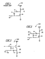
- a prior art control circuit 10 for switching an inductive load includes an active clamp circuit 10A.
- a conventional diode 12 and a zener diode 14 are connected in series, cathode-to-cathode, across the collector-base or drain-gate of a power transistor 16.
- the power transistor 16, shown as a single power MOSFET transistor in Fig. 1 is used to control an inductive load 22 by applying an activating potential to first resistance means comprising a base or gate resistor 18 to switch-on the transistor 16 and hence the inductive load 22 and ground potential to switch-off the transistor 16 and hence the inductive load 22.
- first resistance means comprising a base or gate resistor 18
- the diodes 12, 14 can also be connected anode-to-anode and that more than one power MOSFET or other type power transistor can be used, if required, to meet circuit demands.
- the current through the zener diode 14 is often reduced to such low levels that the zener diode 14 is operated in the "knee" region of its reverse IV characteristic curve. Such low current operation can result in the generation of significant microplasmic noise (MPN) by the zener diode 14.
- MPN microplasmic noise
- Such MPN generated by the zener diode 14 results in momentary high current oscillatory circuit operation of the clamp circuit 10A during clamping operation. This oscillatory circuit operation occurs because a positive feedback path is formed for the transistor 16 by the active clamp circuit 10A, i.e. the conventional diode 12 and the zener diode 14.
- the burst of noise due to the oscillatory operation of the switching control circuit 10 can be coupled into sensitive circuitry associated with the switching control circuit 10 and appear as an extraneous analog or digital input to adversely affect operation of the associated circuitry.
- Fig. 2 shows a control circuit 20 for switching an inductive load.
- Control circuit 20 includes a first embodiment of an improved active clamp circuit 20A in accordance with the present invention. The same identifying numerals have been used in Fig. 2 to identify corresponding elements in the control circuit 20 of Fig. 2.
- the active clamp circuit 20A includes current control means for determining the level of inductive flyback current which flows through the zener diode 14 substantially independently of the operating speed of the control circuit 20.
- the zener diode 14 and the conventional diode 12 are connected anode-to-anode with the anodes being connected to ground potential through second resistance means, comprising a resistor 26 which operates as the current control means.
- a resistor 26 which operates as the current control means.
- an activating potential is applied to the gate resistor 18 to switch-on the transistor 16 and hence the inductive load 22 and ground potential is applied to the gate resistor 18 to switch-off the transistor 16 and hence the inductive load 22.
- the load 22 is switched off, a portion of the energy represented by the flyback voltage is conducted as current through the series connected diodes 12, 14 to partially activate the transistor 16.
- the partial activation of the transistor 16 serves to dissipate or discharge the load 22 in a controlled manner thereby preventing the generation of interfering noise upon switch-off of the load 22.
- the zener breakdown current or current flow through the zener diode 14 is determined by the resistor 26, or more accurately, by the effective parallel combination of the resistor 26 and the resistor 18.
- the current flow through the zener diode 14 is maintained at an appropriate level to prevent the generation of significant MPN levels by selection of the resistor 26.
- the current through the zener diode 14 is controlled primarily by the resistor 26 and the speed of the control circuit 20 is controlled primarily by the resistor 18, substantially independently of one another.
- Fig. 3 shows a control circuit 30 for switching an inductive load.
- Control circuit 30 includes a second embodiment of an improved active clamp circuit 30A in accordance with the present invention. The same identifying numerals have been used in Fig. 3 to identify corresponding elements in the control circuit 30 of Fig. 3.
- the active clamp circuit 30A includes current control means for determining the level of inductive current which flows through the zener diode 14 substantially independently of the operating speed of the control circuit 30.
- the control circuit 30 is shown as including a bipolar PNP power transistor 16A which may be preferred for some applications.
- the zener diode 14 and the conventional diode 12 are connected cathode-to-cathode with the cathodes being means comprising a resistor 26 which operates as the current control means.
- the current through the zener diode 14 of Fig. 3 is controlled primarily by the resistor 26 and the operating speed of the control circuit 30 is controlled primarily by the resistor 18, substantially independently of one another as previously described.
Landscapes
- Electronic Switches (AREA)
- Emergency Protection Circuit Devices (AREA)
Applications Claiming Priority (2)
| Application Number | Priority Date | Filing Date | Title |
|---|---|---|---|
| US462193 | 1990-01-09 | ||
| US07/462,193 US5001373A (en) | 1990-01-09 | 1990-01-09 | Active clamp circuit with immunity to zener diode microplasmic noise |
Publications (3)
| Publication Number | Publication Date |
|---|---|
| EP0437108A2 true EP0437108A2 (fr) | 1991-07-17 |
| EP0437108A3 EP0437108A3 (en) | 1992-03-04 |
| EP0437108B1 EP0437108B1 (fr) | 1997-01-29 |
Family
ID=23835520
Family Applications (1)
| Application Number | Title | Priority Date | Filing Date |
|---|---|---|---|
| EP90314372A Expired - Lifetime EP0437108B1 (fr) | 1990-01-09 | 1990-12-28 | Circuit de commande pour commuter du courant dans une charge |
Country Status (5)
| Country | Link |
|---|---|
| US (1) | US5001373A (fr) |
| EP (1) | EP0437108B1 (fr) |
| JP (1) | JPH04211511A (fr) |
| CA (1) | CA2033236C (fr) |
| DE (1) | DE69029845T2 (fr) |
Cited By (2)
| Publication number | Priority date | Publication date | Assignee | Title |
|---|---|---|---|---|
| DE4432520C1 (de) * | 1994-09-13 | 1996-02-22 | Bosch Gmbh Robert | Elektronische Schutzschaltung gegen Überspannungen an Leistungsschaltelementen |
| CN106027017B (zh) * | 2016-06-29 | 2018-08-14 | 浙江桃园科技有限公司 | 感性负载电压脉宽调制磁性释放电路 |
Families Citing this family (24)
| Publication number | Priority date | Publication date | Assignee | Title |
|---|---|---|---|---|
| JPH04364784A (ja) * | 1991-06-12 | 1992-12-17 | Fuji Electric Co Ltd | Mos型半導体素子駆動回路 |
| DE69416595T2 (de) * | 1994-11-30 | 1999-06-17 | Stmicroelectronics S.R.L., Agrate Brianza, Mailand/Milano | Schaltung zur Begrenzung der Ausgangsspannung eines Leistungstransistors |
| US5500616A (en) * | 1995-01-13 | 1996-03-19 | Ixys Corporation | Overvoltage clamp and desaturation detection circuit |
| JP3464340B2 (ja) * | 1996-04-19 | 2003-11-10 | 沖電気工業株式会社 | 半導体集積回路装置 |
| KR0184568B1 (ko) * | 1996-04-25 | 1999-05-15 | 김광호 | 에스엠피에스의 이상 전원 보호장치 |
| US5723916A (en) * | 1996-05-17 | 1998-03-03 | Delco Electronics Corporation | Electrical load driving device including load current limiting circuitry |
| JPH09321586A (ja) * | 1996-05-29 | 1997-12-12 | Toshiba Microelectron Corp | レベル比較器 |
| US5939908A (en) * | 1996-06-27 | 1999-08-17 | Kelsey-Hayes Company | Dual FET driver circuit |
| US5675478A (en) * | 1996-07-15 | 1997-10-07 | Vari-L Company, Inc. | Oscillator voltage regulator |
| US5812006A (en) * | 1996-10-29 | 1998-09-22 | Texas Instruments Incorporated | Optimized power output clamping structure |
| US6169439B1 (en) * | 1997-01-02 | 2001-01-02 | Texas Instruments Incorporated | Current limited power MOSFET device with improved safe operating area |
| JP3814958B2 (ja) * | 1997-07-09 | 2006-08-30 | 日産自動車株式会社 | 半導体集積回路 |
| US5920224A (en) * | 1998-02-17 | 1999-07-06 | Harris Corporation | Network for improving electro-magnetic interference response |
| US6091274A (en) * | 1998-02-17 | 2000-07-18 | Intersil Corporation | Optimum placement of bypass capacitors in a network for improving electro-magnetic interference response |
| US7365584B2 (en) * | 2006-06-02 | 2008-04-29 | Freescale Semiconductor, Inc. | Slew-rate control apparatus and methods for a power transistor to reduce voltage transients during inductive flyback |
| JP4432953B2 (ja) * | 2006-09-27 | 2010-03-17 | 株式会社日立製作所 | 半導体電力変換装置 |
| US8189309B2 (en) | 2009-07-17 | 2012-05-29 | Texas Instruments Incorporated | Clamp for controlling current discharge |
| JP5492518B2 (ja) * | 2009-10-02 | 2014-05-14 | 株式会社日立製作所 | 半導体駆動回路、及びそれを用いた半導体装置 |
| US8970265B2 (en) * | 2013-03-14 | 2015-03-03 | Allegro Microsystems, Llc | Systems and methods for driving a load under various power conditions |
| JP6371739B2 (ja) * | 2015-08-05 | 2018-08-08 | 日立オートモティブシステムズ株式会社 | 誘導性負荷駆動装置 |
| TWI625919B (zh) * | 2016-12-23 | 2018-06-01 | 財團法人工業技術研究院 | 電源保持電路裝置 |
| US10230356B2 (en) | 2017-02-27 | 2019-03-12 | Allegro Microsystems, Llc | High-side output transistor circuit |
| JP7435359B2 (ja) * | 2020-08-24 | 2024-02-21 | 株式会社デンソー | 負荷駆動回路 |
| US12206392B2 (en) | 2023-06-21 | 2025-01-21 | Rockwell Automation Technologies, Inc. | Transient overvoltage active clamping for semiconductor power switches |
Family Cites Families (18)
| Publication number | Priority date | Publication date | Assignee | Title |
|---|---|---|---|---|
| US3010031A (en) * | 1956-10-24 | 1961-11-21 | Research Corp | Symmetrical back-clamped transistor switching sircuit |
| US3249808A (en) * | 1961-09-21 | 1966-05-03 | Gen Motors Corp | Ignition system |
| US3217310A (en) * | 1961-12-14 | 1965-11-09 | Honeywell Inc | Discharge circuitry for voltage doubling and switching circuitry |
| US3277312A (en) * | 1963-07-03 | 1966-10-04 | Singer Co | Differential response circuit |
| US3641407A (en) * | 1970-10-26 | 1972-02-08 | Teletype Corp | Inductor surge protection for transistors |
| FR2352448A1 (fr) * | 1976-05-21 | 1977-12-16 | Ibm France | Amplificateur d'alimentation d'une charge inductive |
| DE2811149A1 (de) * | 1978-03-15 | 1979-09-20 | Bosch Gmbh Robert | Elektrischer stromkreis mit einem schalttransistor und mit einem induktiven widerstand, insbesondere mit der primaerwicklung einer zu einer brennkraftmaschine gehoerenden zuendspule |
| JPS56122132U (fr) * | 1980-02-18 | 1981-09-17 | ||
| DE3026040C2 (de) * | 1980-07-09 | 1982-05-27 | Siemens AG, 1000 Berlin und 8000 München | Schalter mit in Serie geschalteten MOS-FET |
| US4492883A (en) * | 1982-06-21 | 1985-01-08 | Eaton Corporation | Unpowered fast gate turn-off FET |
| US4547686A (en) * | 1983-09-30 | 1985-10-15 | The United States Of America As Represented By The Administrator Of The National Aeronautics And Space Administration | Hybrid power semiconductor switch |
| DE3409423A1 (de) * | 1984-03-15 | 1985-09-26 | Philips Patentverwaltung Gmbh, 2000 Hamburg | Schaltungsanordnung zum schalten des stromes in einer induktiven last |
| US4658203A (en) * | 1984-12-04 | 1987-04-14 | Airborne Electronics, Inc. | Voltage clamp circuit for switched inductive loads |
| US4665459A (en) * | 1985-04-01 | 1987-05-12 | Motorola, Inc. | Method and circuit for dissipating stored inductive energy |
| JPS61288616A (ja) * | 1985-06-17 | 1986-12-18 | Fuji Electric Co Ltd | 半導体装置 |
| US4679112A (en) * | 1986-07-31 | 1987-07-07 | General Motors Corporation | Transistor protection circuit for automotive motor control applications |
| US4750078A (en) * | 1987-06-15 | 1988-06-07 | Motorola, Inc. | Semiconductor protection circuit having both positive and negative high voltage protection |
| US4894567A (en) * | 1988-10-17 | 1990-01-16 | Honeywell Inc. | Active snubber circuit |
-
1990
- 1990-01-09 US US07/462,193 patent/US5001373A/en not_active Expired - Fee Related
- 1990-12-27 CA CA002033236A patent/CA2033236C/fr not_active Expired - Fee Related
- 1990-12-28 DE DE69029845T patent/DE69029845T2/de not_active Expired - Lifetime
- 1990-12-28 EP EP90314372A patent/EP0437108B1/fr not_active Expired - Lifetime
-
1991
- 1991-01-08 JP JP3000671A patent/JPH04211511A/ja active Pending
Cited By (2)
| Publication number | Priority date | Publication date | Assignee | Title |
|---|---|---|---|---|
| DE4432520C1 (de) * | 1994-09-13 | 1996-02-22 | Bosch Gmbh Robert | Elektronische Schutzschaltung gegen Überspannungen an Leistungsschaltelementen |
| CN106027017B (zh) * | 2016-06-29 | 2018-08-14 | 浙江桃园科技有限公司 | 感性负载电压脉宽调制磁性释放电路 |
Also Published As
| Publication number | Publication date |
|---|---|
| CA2033236A1 (fr) | 1991-07-10 |
| US5001373A (en) | 1991-03-19 |
| CA2033236C (fr) | 1997-04-29 |
| EP0437108A3 (en) | 1992-03-04 |
| DE69029845T2 (de) | 1997-09-18 |
| EP0437108B1 (fr) | 1997-01-29 |
| DE69029845D1 (de) | 1997-03-13 |
| JPH04211511A (ja) | 1992-08-03 |
Similar Documents
| Publication | Publication Date | Title |
|---|---|---|
| US5001373A (en) | Active clamp circuit with immunity to zener diode microplasmic noise | |
| US5091664A (en) | Insulated gate bipolar transistor circuit with overcurrent protection | |
| US6275093B1 (en) | IGBT gate drive circuit with short circuit protection | |
| EP0599605A2 (fr) | Dispositif semi-conducteur ayant une fonction de détection de courant | |
| US6236122B1 (en) | Load drive device | |
| US4841166A (en) | Limiting shoot-through current in a power MOSFET half-bridge during intrinsic diode recovery | |
| US7701279B2 (en) | Driving circuit for an emitter-switching configuration | |
| EP1037387B1 (fr) | Circuit d'attaque de grille stabilisé | |
| US4388499A (en) | Line interruption circuit for use in a telephone set | |
| US4556838A (en) | Electronic switch | |
| US5457419A (en) | MOSFET with temperature protection | |
| EP0352828A2 (fr) | Circuit de commande de la tension de limitation d'une charge inductive attaquée par un dispositif de puissance en configuration d'attaque du côté de la tension | |
| EP0388616B1 (fr) | Circuit de protection à maximum d'intensité pour un dispositif électrostatique à débrayage automatique | |
| US20010040480A1 (en) | Switching device with separated driving signal input and driving circuit of the same | |
| US5889390A (en) | Circuit arrangement for converting a DC voltage into another DC voltage with simultaneous regulation of the emittable voltage at a predetermined value | |
| GB2053606A (en) | Improvements in and relating to semiconductor switching circuits | |
| US5945868A (en) | Power semiconductor device and method for increasing turn-on time of the power semiconductor device | |
| US6388530B1 (en) | Microwave amplifier implemented by heterojunction field effect transistors | |
| US5453900A (en) | Protective circuit for a power MOSFET that drives an inductive load | |
| US7012469B2 (en) | Integrated circuit device having high efficiency at the time of low power output | |
| US6169431B1 (en) | Drive circuit for a controllable semiconductor component | |
| US5027020A (en) | Zero voltage switching AC relay circuit | |
| US4642483A (en) | Reverse bias current supply system for a switching device | |
| US4047054A (en) | Thyristor switching circuit | |
| KR100354726B1 (ko) | 집적형 전력 증폭단을 제어하기 위한 방법 및 장치 |
Legal Events
| Date | Code | Title | Description |
|---|---|---|---|
| PUAI | Public reference made under article 153(3) epc to a published international application that has entered the european phase |
Free format text: ORIGINAL CODE: 0009012 |
|
| AK | Designated contracting states |
Kind code of ref document: A2 Designated state(s): DE FR GB |
|
| PUAL | Search report despatched |
Free format text: ORIGINAL CODE: 0009013 |
|
| AK | Designated contracting states |
Kind code of ref document: A3 Designated state(s): DE FR GB |
|
| 17P | Request for examination filed |
Effective date: 19920827 |
|
| 17Q | First examination report despatched |
Effective date: 19950418 |
|
| GRAG | Despatch of communication of intention to grant |
Free format text: ORIGINAL CODE: EPIDOS AGRA |
|
| GRAH | Despatch of communication of intention to grant a patent |
Free format text: ORIGINAL CODE: EPIDOS IGRA |
|
| GRAH | Despatch of communication of intention to grant a patent |
Free format text: ORIGINAL CODE: EPIDOS IGRA |
|
| GRAA | (expected) grant |
Free format text: ORIGINAL CODE: 0009210 |
|
| AK | Designated contracting states |
Kind code of ref document: B1 Designated state(s): DE FR GB |
|
| ET | Fr: translation filed | ||
| REF | Corresponds to: |
Ref document number: 69029845 Country of ref document: DE Date of ref document: 19970313 |
|
| PGFP | Annual fee paid to national office [announced via postgrant information from national office to epo] |
Ref country code: DE Payment date: 19971021 Year of fee payment: 8 |
|
| PGFP | Annual fee paid to national office [announced via postgrant information from national office to epo] |
Ref country code: GB Payment date: 19971126 Year of fee payment: 8 |
|
| PLBE | No opposition filed within time limit |
Free format text: ORIGINAL CODE: 0009261 |
|
| STAA | Information on the status of an ep patent application or granted ep patent |
Free format text: STATUS: NO OPPOSITION FILED WITHIN TIME LIMIT |
|
| PGFP | Annual fee paid to national office [announced via postgrant information from national office to epo] |
Ref country code: FR Payment date: 19971215 Year of fee payment: 8 |
|
| 26N | No opposition filed | ||
| PG25 | Lapsed in a contracting state [announced via postgrant information from national office to epo] |
Ref country code: DE Free format text: LAPSE BECAUSE OF THE APPLICANT RENOUNCES Effective date: 19981126 |
|
| PG25 | Lapsed in a contracting state [announced via postgrant information from national office to epo] |
Ref country code: GB Free format text: LAPSE BECAUSE OF NON-PAYMENT OF DUE FEES Effective date: 19981228 |
|
| GBPC | Gb: european patent ceased through non-payment of renewal fee |
Effective date: 19981228 |
|
| PG25 | Lapsed in a contracting state [announced via postgrant information from national office to epo] |
Ref country code: FR Free format text: LAPSE BECAUSE OF NON-PAYMENT OF DUE FEES Effective date: 19990831 |
|
| REG | Reference to a national code |
Ref country code: FR Ref legal event code: ST |