EP0437218A2 - Prüfvorrichtung für einen Halbleiterspeicher - Google Patents
Prüfvorrichtung für einen Halbleiterspeicher Download PDFInfo
- Publication number
- EP0437218A2 EP0437218A2 EP91100112A EP91100112A EP0437218A2 EP 0437218 A2 EP0437218 A2 EP 0437218A2 EP 91100112 A EP91100112 A EP 91100112A EP 91100112 A EP91100112 A EP 91100112A EP 0437218 A2 EP0437218 A2 EP 0437218A2
- Authority
- EP
- European Patent Office
- Prior art keywords
- logical
- multiplexers
- results
- memory devices
- output
- Prior art date
- Legal status (The legal status is an assumption and is not a legal conclusion. Google has not performed a legal analysis and makes no representation as to the accuracy of the status listed.)
- Withdrawn
Links
Images




Classifications
-
- G—PHYSICS
- G11—INFORMATION STORAGE
- G11C—STATIC STORES
- G11C29/00—Checking stores for correct operation ; Subsequent repair; Testing stores during standby or offline operation
- G11C29/56—External testing equipment for static stores, e.g. automatic test equipment [ATE]; Interfaces therefor
-
- G—PHYSICS
- G01—MEASURING; TESTING
- G01R—MEASURING ELECTRIC VARIABLES; MEASURING MAGNETIC VARIABLES
- G01R31/00—Arrangements for testing electric properties; Arrangements for locating electric faults; Arrangements for electrical testing characterised by what is being tested not provided for elsewhere
- G01R31/28—Testing of electronic circuits, e.g. by signal tracer
- G01R31/317—Testing of digital circuits
- G01R31/3181—Functional testing
- G01R31/319—Tester hardware, i.e. output processing circuits
- G01R31/3193—Tester hardware, i.e. output processing circuits with comparison between actual response and known fault free response
- G01R31/31935—Storing data, e.g. failure memory
Definitions
- the present invention relates to a semiconductor memory tester which has an arrangement in which a test pattern is applied to each of a plurality of memory devices under test mounted on a test head, the output from each memory device is subjected to a logical comparison with an expected value for each pin and the result of logical comparison is stored in a fail memory.
- Fig. 1 shows a portion of a semiconductor memory tester of this kind.
- Memory devices under test A1 and A2 are mounted on a first test head 11A and memory devices B1 and B2 are mounted on a second test head 11B.
- a test pattern, i.e. data and an address, from a pattern generator 15 is applied to the memory devices A1, A2, B1 and B2, in which the data is written at the address and from which the thus written data is read out into logical comparators 161, 162, 171 and 172 for comparison with expected values for each pin.
- the compared results are output from the comparators 161, 162, 171 and 172.
- Fig. 2 in which the results of logical comparison for only first pins of the memory devices A1, A2, B1 and B2 are shown, compared outputs A11 and A21 for the first pins of the memory devices A1 and A2 on the first test head 11A are both applied to multiplexers 181 and 182.
- the multiplexer 181 responds to a select signal S1 to select and output one of the two inputs thereto, and the multiplexer 182 similarly responds to a select signal S2 to select and output one of the two inputs thereto.
- the results of comparison B11 and B21 for the first pins of the memory devices B1 and B2 on the second test head 11B are both provided to multiplexers 211 and 212.
- the multiplexer 211 responds to a select signal S3 to select and output one of the two inputs thereto, and the multiplexer 212 responds to a select signal S4 to select and output one of the two inputs thereto.
- the outputs of the multiplexers 181 and 211 are input into a multiplexer 231, which responds to a select signal S5 to select and output one of the inputs.
- the outputs of the multiplexers 182 and 212 are input into a multiplexer 232, which responds to a select signal S6 to select and output one of the inputs.
- the outputs of the multiplexers 231 and 232 are stored in fail memories 251 and 252, respectively.
- the comparison result A11 is stored in the fail memory 251
- the comparison result B21 is stored in the fail memory 252.
- multiplexers similar to those 181, 182, 211, 212, 231 and 232 though not shown, and the fail memories 251 and 252 are adapted to store at respective addresses the results of logical comparisons corresponding to respective pins.
- test heads 11A and 11B In the case where only one of the test heads 11A and 11B, for example, 11A, the results of logical comparisons for the two memory devices A1 and A2 loaded on the test head 11A can concurrently be stored in the fail memories 251 and 252.
- the both test heads 11A and 11B are used, the following problems exist:
- the results of logical comparisons for a predetermined plurality of pins of each of N are ORed by a first OR circuit
- the results of logical comparisons for a predetermined plurality of pins of each of N memory devices under test on a second test head are ORed by a second OR circuit.
- a desired one of N+1 outputs including the results of logical comparisons for the corresponding pins of the N memory devices on the first test head and the output of the first OR circuit, corresponding to one of the N memory devices, is selected by a first multiplexer.
- a desired one of N+1 outputs including the results of logical comparisons for the corresponding pins of the N memory devices on the second test head and the output of the second OR circuit, corresponding to one of the N memory devices, is selected by a second multiplexer.
- One of the outputs of the first and second multiplexers for each of the corresponding pins is selected by one of third multiplexers, and the outputs of these third multiplexers are stored in a plurality of fail memories.
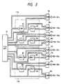
- the first test head 11A carries four memory devices under test A1 to A4 and the second test head 11B carries four memory devices under test B1 to B4.
- a test pattern composed of data and an address is applied from the pattern generator 15 to the memory devices A1 to A4 and B1 to B4, wherein the data is written at the address.
- the data thus written in the memory devices under test is read out therefrom and provided to logical comparators 161 to 164 and 171 to 174 for logical comparison with expected values for each pin.
- the results of such logical comparisons are stored in fail memories.
- the memory devices A1 to A4 and B1 to B4 each have four output pins and the results of logical comparisons A11 to A14, A21 to A24, A31 to A34, A41 to A44 and B11 to B14, B21 to B24, B31 to B34, B41 to B44 are selectively stored in the fail memories as described below.
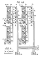
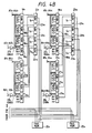
- Fig. 4 illustrates an example of a multiplexer circuit constructed so that the results of logical comparisons output from the logical comparators 161, to 164 and 171 to 174 in Fig. 3 can selectively be stored in fail memories 251 to 254 as in the prior art and that, if necessary, the logical sums (i.e. logical OR's) of the results of logical comparisons corresponding to the plurality of pins of the memory devices can selectively stored in the fail memories 251 to 254 according to the present invention.
- the logical sums i.e. logical OR's
- first multiplexers 181 to 184 are supplied with the results of logical comparisons A11, A21, A31 and A41 corresponding to first pins of the memory devices A1 to A4 loaded on the first test head 11A depicted in Fig. 3, respectively.
- the results of logical comparisons A11, A12, A13 and A14 corresponding to the four output pins of the memory device A1 are ORed by a first OR circuit 271 and the resulting logical sum ORA1 is also provided to the multiplexers 181 to 184.
- the first multiplexer 181 Based on select signals a1, b1 and c1 applied thereto, selects and outputs any one of the four results of logical comparisons A11 to A41 and the logical sum ORA1.
- the first multiplexers 182, 183 and 184 each select and output any one of the four results of logical comparisons A11 to A41 and the logical sum ORA1, based on the select signals (a2, b2, c2), (a3, b3, c3) and (a4, b4, c4), respectively.
- first multiplexers 185 to 188 are each supplied with the results of logical comparisons A12, A22, A32 and A42 corresponding to second output pins of the memory devices A1 to A4 and a logical sum ORA2 of the results of logical comparisons corresponding to the four output pins of the memory device A2 and provided from a first OR circuit 272, and one of the five inputs to each of the first multiplexers 185 to 188 is selected and output therefrom in accordance with the select signals (a1, b1, c1), (a2, b2, c2), (a3, b3, c3) and (a4, b4, c4), respectively.
- First multiplexers 189 to 1812 are each supplied with the results of logical comparisons A13, A23, A33 and A43 corresponding to third output pins of the memory devices A1 to A4 and a logical sum ORA3 of the results of logical comparisons corresponding to the four output pins of the memory device A3 and provided from a first OR circuit 273, and one of the five inputs to each of the first multiplexers 189 to 1812 is selected and output.
- First multiplexers 1813 to 1816 are each supplied with the results of logical comparisons A14, A24, A34 and A44 corresponding to fourth output pins of the memory devices A1 to A4 and a logical sum ORA4 of the results of logical comparisons corresponding to the four output pins of the memory device A4 provided from a first OR circuit 274, and the first multiplexers 1813 to 1816 each selectively output one of such five inputs thereto in the same manner as referred to above.
- second multiplexers 211 to 214, 215 to 218, 219 to 2112 and 2113 to 2116 are supplied with the results of logical comparisons B11 to B41, B12 to B42, B13 to B43 and B14 to B44 for the corresponding output pins of the memory devices B1 to B4 loaded on the test head 11B and logical sums ORB1 to ORB4 of the results of logical comparisons corresponding to the four output pins of each of the memory devices B1 to B4 provided from second OR circuits 281 to 284, respectively.
- the second multiplexers each selectively output one of such five inputs thereto.
- a third multiplexer 231 is supplied with the selected outputs from the first multiplexer 181 associated with the first test head 11A and the second multiplexer 211 associated with the second test head 11B and selectively outputs one of the two inputs in accordance with the select signal S1.
- a third multiplexer 232 is supplied with the selected outputs from the first and second multiplexers 182 and 212 and selectively outputs either one of the two inputs in accordance with the select signal S2.
- a third multiplexer 233 is supplied with the selected outputs from the first and second multiplexers 183 and 213 and selectively outputs either one of the two inputs in accordance with a select signal S3.
- a third multiplexer 234 is supplied with the selected outputs from the first and second multiplexers 184 and 214 and selectively outputs either one of the two inputs in accordance with a select signal S4.
- each of third multiplexers 235 to 238, 239 to 2312 and 2313 to 2316 is also supplied with the selected outputs from the first and second multiplexers associated with the first and second test heads 11A and 11B, respectively, and selectively outputs either one of the two inputs in accordance with corresponding one of select signals S1 to S4.
- the selected outputs from the third multiplexers 231 to 234 are provided as first bit inputs to fail memories 251 to 254; the selected outputs from the third multiplexers 235 to 238 are provided as second bit inputs to the fail memories 251 to 254; the selected outputs from the third multiplexers 239 to 2312 are provided as third bit inputs to the fail memories 251 to 254; and the selected outputs from the third multiplexers 2312 to 2316 are provided as fourth bit inputs to the fail memories 251 to 254.
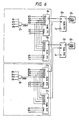
- Figs. 5 and 6 show concrete circuits interconnecting the OR circuits 271 and 281, the first multiplexers 181 to 184, the second multiplexers 211 to 214, the third multiplexers 231 to 234 and the fail memories 251 to 254 in Fig. 4.
- Fig. 6 shows concrete circuits interconnecting the OR circuits 271 and 281, the first multiplexers 181 to 184, the second multiplexers 211 to 214, the third multiplexers 231 to 234 and the fail memories 251 to 254 in Fig. 4.
- FIG. 6 shows concrete circuits interconnecting the OR circuits 271 and 281, the first multiplexers 181 to 184, the second multiplexers 211 to 214, the third multiplexers 231 to 234 and the fail memories 251 to 254 in Fig. 4.
- FIG. 6 shows concrete circuits interconnecting the OR circuits 271 and 281, the first multiplexers 181 to 184, the second multiplexers 211 to 214, the third multiplexers 231
- the results of logical comparisons A11 to A41 corresponding to the first output pins of the memory devices 121 to 124 carried by the first test head 11A are input into the first multiplexers 181, 182, 183 and 184, respectively.
- the results of logical comparisons A11 to A14 corresponding to the first to fourth output pins of the first memory device 121 mounted on the first test head 11A are ORed by the first OR circuit 271 and its output ORA1 is applied to each of the first multiplexers 181 to 184.
- the first multiplexer 181 responds to the select signals a1 and b1 to select and output any one of the inputs A11 to A41 and, when the select signal c1 is high, outputs the output ORA1 from the first OR circuit 271.
- the first multiplexer 182 responds to the select signals a2 and b2 to select and output any one of the inputs A11 to A41 and, when the select signal c2 is high, outputs the output ORA1 from the first OR circuit 271.
- the first multiplexer 183 responds to the select signals a3 and b3 to select and output any one of the inputs A11 to A41 and, when the select signal c3 is high, outputs the output ORA1 from the first OR circuit 271.
- the first multiplexer 184 responds to the select signals a4 and b4 to select and output any one of the inputs A11 to A41 and, when the select signal c4 is high, outputs the output ORA1 from the first OR circuit 271.
- the results of logical comparisons B11 to B41 corresponding to the first output pins of the memory devices 141 to 144 carried by the second test head 11B are input into the second multiplexers 211, 212, 213 and 214, respectively.
- the results of logical comparisons corresponding to the first to fourth output pins of the first memory device 141 mounted on the second test head 11B are ORed by the second OR circuit 281 and its output ORB1 is applied to each of the second multiplexers 211 to 214.
- the second multiplexers 211 to 214 each selectively output any one of the five inputs in accordance with the select signals (a1, b1, c1), ... (a4, b4, c4).
- the outputs of the first and second multiplexers 181 and 211 are input into the third multiplexer 231 and either one of the two inputs is selectively output therefrom in accordance with the select signal S1; the outputs of the first and second multiplexers 182 and 212 are input into the third multiplexer 232 and either one of the two inputs is selectively output therefrom in accordance with the select signal S2; the outputs of the first and second multiplexers 183 and 213 are input into the third multiplexer 233 and either one of the two inputs is selectively output therefrom in accordance with the select signal S3; and the outputs of the first and second multiplexers 184 and 214 are input into the third multiplexer 234 and either one of the two inputs is selectively output therefrom in accordance with the select signal S4.
- the outputs of the third multiplexers 231 to 234 are stored in the fail memories 251 and 254, respectively.
- the connections of the first multiplexers 185 to 188, the second multiplexers 215 to 218 and the third multiplexers 235 to 238 in Fig. 4 are similar to those shown in Figs. 5 and 6. Further, the first multiplexers 189 to 1812, the second multiplexers 219 to 2112, the third multiplexers 239 to 2312 and the first multiplexers 1813 to 1816, the second multiplexers 2113 to 2116, the third multiplexers 2313 to 2316 are also connected in a manner similar to those shown in Figs. 5 and 6. Hence, these circuit connections are not shown, for the sake of brevity.
- Table I in Fig. 7 shows, by way of example, the selected outputs of the first and second multiplexers 181 to 184 and 211 to 214 and the selection of the third multiplexers 231 to 234 in response to the application thereto of the select signals identified by a, b, c and S.
- a horizontal column labeled "1st MPX" shows the five inputs A11 to A41 and ORA1 to the first multiplexers 181 to 184 associated with the first test head 11A and selected outputs corresponding to combinations of the select signals (a, b, c).
- Another horizontal column labeled "2nd MPX” shows the five inputs B11 to B41 and ORB1 to the second multiplexers 211 to 214 associated with the second test head 11B and selected outputs corresponding to combinations of the select signals (a, b, c).
- a vertical column labeled “3rd MPX” shows the multiplexer outputs which the third multiplexers 231 to 234 select in accordance with the select signal S.
- the selected outputs based on the select signals a, b, c and S can easily be determined in the same manner as described above in respect of Table I. Hence, such selected outputs are not shown.
- the outputs A11, A21, A31 and A41 are selected, respectively; in the first multiplexers 185, 186, 187 and 188 the outputs A12, A22, A32 and A42 are selected, respectively; in the first multiplexers 189, 1810, 1811 and 1812 the outputs A13, A23, A33 and A43 are selected, respectively; and in the first multiplexers 1813, 1814, 1815 and 1816 the outputs A14, A24, A34 and A44 are selected, respectively.
- the third multiplexers 231 to 2316 all select the first test head 11 side (the first multiplexer outputs), the results of logical comparisons A11 to A14 of the memory device 121 are stored in the fail memory 251; the results of logical comparisons A21 to A24 of the memory device 122 are stored in the fail memory 252; the results of logical comparisons A31 to A34 of the memory device 123 are stored in the fail memory 253; and the results of logical comparisons A41 to A44 of the memory device 124 are stored in the fail memory 254.
- the results of logical comparisons of the memory devices 121 to 124 are stored individually in the fail memories 251 to 254.
- the select signals (a1, b1, c1), ... (a4, b4, c4) for the second multiplexers 211 to 2116 have the same values as in the above case and the select signals S1, S2, S3 and S4 are all set to 1, the third multiplexers 231 to 2316 select the second test head 11B side (the second multiplexer outputs), and consequently, the results of logical comparisons B11 to B14 of the memory device 141, the results of logical comparisons B21 to B24 of the memory device 142, the results of logical comparisons B31 to B34 of the memory device 143 and the results of logical comparisons B41 to B44 of the memory device 144 are stored in the fail memories 251, 252, 253 and 254, respectively. That is, the results of logical comparisons of the memory devices 141 to 144 are stored individually in the fail memories 251 to 254.
- the third multiplexer 231 provides the output ORA1 of the first OR circuit 271 and, similarly, the third multiplexers 235, 239 and 2313 provide the outputs ORA2, ORA3 and ORA4 of the first OR circuits 272, 273 and 274, respectively.
- the outputs of the third multiplexers 231, 235, 239 and 2313 are stored in the fail memory 251. Furthermore, the third multiplexer 232 provides the output ORB1 of the second OR circuit 281, the third multiplexers 236, 2310 and 2314 provide the outputs ORB2, ORB3 and ORB4 of the second OR circuits 282, 283 and 284, respectively, and the outputs of the third multiplexers 232, 236, 2310 and 2314 are stored in the fail memory 252.
- the logical sums ORA1, ORA2, ORA3 and ORA4 of the results of logical comparisons A11 to A14, A21 to A24, A31 to A34 and A41 to A44 of the memory devices 121, 122, 123 and 124 loaded on the first test head 11A are stored in the fail memory 251.
- the logical sums ORB1, ORB2, ORB3 and ORB4 of the results of logical comparisons B11 to B14, B21 to B24, B31 to B34 and B41 to B44 of the memory devices 141, 142, 143 and 144 loaded on the second test head 11B are stored in the fail memory 252.
- the results of logical comparisons of the memory devices on the first and second test heads 11A and 11B can be stored in the fail memories 251 and 252 concurrently.
- the OR of the results of logical comparisons corresponding to the first to fourth output pins of each memory device can be known, that is, the results of logical comparisons for each pin are not stored in the fail memory.
- the above embodiment has been described to include two test heads, but the number of test heads is not limited specifically thereto but may be one or more than two. While the above embodiment has been described in connection with the case where four memory devices under test are loaded on each test head and each have four output pins, it can also be considered that the memory devices A1 and A2 in Fig. 3, for example, are those into which one memory device having eight output pins has been provisionally divided for test. The same is true of the memory devices A3, A4, B1, B2, B3 and B4.
- the number of fail memories need not always be four but needs only to be equal to at least the number of test heads used.
- the results of logical comparisons corresponding to a plurality of pins of each memory device are ORed and the OR is selectable.
- the results of logical comparisons corresponding to each pin of a plurality of memory device on each test head can be stored in separate fail memories as in the prior art, besides, by selecting the above-mentioned OR, the results of tests of the memory devices on first and second test heads can be stored in separate fail memories concurrently.
Landscapes
- Tests Of Electronic Circuits (AREA)
- Test And Diagnosis Of Digital Computers (AREA)
- For Increasing The Reliability Of Semiconductor Memories (AREA)
Applications Claiming Priority (2)
| Application Number | Priority Date | Filing Date | Title |
|---|---|---|---|
| JP4095/90 | 1990-01-10 | ||
| JP2004095A JP2831767B2 (ja) | 1990-01-10 | 1990-01-10 | 半導体メモリ試験装置 |
Publications (2)
| Publication Number | Publication Date |
|---|---|
| EP0437218A2 true EP0437218A2 (de) | 1991-07-17 |
| EP0437218A3 EP0437218A3 (en) | 1992-04-29 |
Family
ID=11575235
Family Applications (1)
| Application Number | Title | Priority Date | Filing Date |
|---|---|---|---|
| EP19910100112 Withdrawn EP0437218A3 (en) | 1990-01-10 | 1991-01-02 | Semiconductor memory tester |
Country Status (4)
| Country | Link |
|---|---|
| US (1) | US5216673A (de) |
| EP (1) | EP0437218A3 (de) |
| JP (1) | JP2831767B2 (de) |
| KR (1) | KR950001292B1 (de) |
Cited By (2)
| Publication number | Priority date | Publication date | Assignee | Title |
|---|---|---|---|---|
| EP0819275A4 (de) * | 1995-03-17 | 1998-10-14 | Aehr Test Systems Inc | Verfahren und einrichtung zum prüfen von speicherprogrammiereinrichtungen |
| US7337381B2 (en) * | 2003-04-16 | 2008-02-26 | Advantest Corporation | Memory tester having defect analysis memory with two storage sections |
Families Citing this family (11)
| Publication number | Priority date | Publication date | Assignee | Title |
|---|---|---|---|---|
| WO1995030227A1 (en) * | 1994-04-29 | 1995-11-09 | Texas Instruments Incorporated | A method and apparatus for testing a memory circuit with parallel block write operation |
| US5610925A (en) * | 1995-03-27 | 1997-03-11 | Advantest Corporation | Failure analyzer for semiconductor tester |
| JP2991138B2 (ja) * | 1996-12-09 | 1999-12-20 | 日本電気株式会社 | メモリlsiの不良解析方法 |
| DE19921756A1 (de) * | 1998-05-13 | 1999-11-25 | Advantest Corp | Speichertestvorrichtung und Datenselektionsschaltkreis |
| JP4156726B2 (ja) * | 1998-10-16 | 2008-09-24 | 株式会社アドバンテスト | 高速パターン生成方法及び装置並びにメモリ試験装置 |
| US6405333B1 (en) * | 1999-03-31 | 2002-06-11 | Teradyne, Inc. | Fail array memory control circuit with selective input disable |
| US6694461B1 (en) * | 1999-07-26 | 2004-02-17 | Ati International Srl | System and method for testing integrated memories |
| US6868513B1 (en) * | 2000-10-26 | 2005-03-15 | International Business Machines Corporation | Automated multi-device test process and system |
| US6757209B2 (en) * | 2001-03-30 | 2004-06-29 | Intel Corporation | Memory cell structural test |
| US7239971B2 (en) * | 2004-04-16 | 2007-07-03 | Formfactor, Inc. | Method and apparatus for calibrating communications channels |
| JP2022117853A (ja) * | 2021-02-01 | 2022-08-12 | パナソニックIpマネジメント株式会社 | 診断回路、電子デバイス及び診断方法 |
Family Cites Families (5)
| Publication number | Priority date | Publication date | Assignee | Title |
|---|---|---|---|---|
| JPS59180898A (ja) * | 1983-03-31 | 1984-10-15 | Hitachi Ltd | 不良ビット救済方法 |
| EP0218830B1 (de) * | 1985-09-09 | 1992-04-29 | Hitachi, Ltd. | Speicherprüfgerät |
| JPS62170094A (ja) * | 1986-01-21 | 1987-07-27 | Mitsubishi Electric Corp | 半導体記憶回路 |
| US4730318A (en) * | 1986-11-24 | 1988-03-08 | International Business Machines Corporation | Modular organized storage tester |
| US5025205A (en) * | 1989-06-22 | 1991-06-18 | Texas Instruments Incorporated | Reconfigurable architecture for logic test system |
-
1990
- 1990-01-10 JP JP2004095A patent/JP2831767B2/ja not_active Expired - Fee Related
-
1991
- 1991-01-02 EP EP19910100112 patent/EP0437218A3/en not_active Withdrawn
- 1991-01-03 US US07/637,323 patent/US5216673A/en not_active Expired - Lifetime
- 1991-01-07 KR KR1019910000104A patent/KR950001292B1/ko not_active Expired - Fee Related
Cited By (2)
| Publication number | Priority date | Publication date | Assignee | Title |
|---|---|---|---|---|
| EP0819275A4 (de) * | 1995-03-17 | 1998-10-14 | Aehr Test Systems Inc | Verfahren und einrichtung zum prüfen von speicherprogrammiereinrichtungen |
| US7337381B2 (en) * | 2003-04-16 | 2008-02-26 | Advantest Corporation | Memory tester having defect analysis memory with two storage sections |
Also Published As
| Publication number | Publication date |
|---|---|
| KR950001292B1 (ko) | 1995-02-15 |
| JP2831767B2 (ja) | 1998-12-02 |
| JPH03209183A (ja) | 1991-09-12 |
| US5216673A (en) | 1993-06-01 |
| EP0437218A3 (en) | 1992-04-29 |
Similar Documents
| Publication | Publication Date | Title |
|---|---|---|
| US4680733A (en) | Device for serializing/deserializing bit configurations of variable length | |
| US5432797A (en) | IC tester having a pattern selector capable of selecting pins of a device under test | |
| US5644578A (en) | Failure memory device | |
| JPS5975346A (ja) | ラッチ列制御システム | |
| US5216673A (en) | Semiconductor memory tester | |
| US4370746A (en) | Memory address selector | |
| KR930011107B1 (ko) | 불량 메모리셀 존재를 표시하는 정보를 갖는 반도체 메모리 장치 | |
| EP0366553A2 (de) | Prüfgerät und -verfahren zur Prüfung eines elektronischen Geräts und Halbleitergerät mit diesem Prüfgerät | |
| KR920003322A (ko) | 개선된 테스트 모드를 가지는 반도체 메모리 | |
| US4969126A (en) | Semiconductor memory device having serial addressing and operating method thereof | |
| US5561429A (en) | Content limit addressable memory | |
| EP0136178A2 (de) | Automatische Speicherkarten-Rekonfiguration | |
| EP0437217B1 (de) | Speicherprüfgerät | |
| US6061813A (en) | Memory test set | |
| EP0071315A2 (de) | Digitales Datengerät mit peripherer Einheiten auswahl | |
| US6198669B1 (en) | Semiconductor integrated circuit | |
| EP0398816A2 (de) | Testmethode, Testschaltung und integrierter Halbleiterschaltkreis mit Testschaltung | |
| US5555214A (en) | Apparatus for serial reading and writing of random access memory arrays | |
| EP0043415A1 (de) | Speicherprüfer | |
| US4322812A (en) | Digital data processor providing for monitoring, changing and loading of RAM instruction data | |
| US6907385B2 (en) | Memory defect redress analysis treating method, and memory testing apparatus performing the method | |
| US6092227A (en) | Test circuit | |
| US5825787A (en) | System and method for accessing a test vector memory | |
| US4599721A (en) | Programmable cross bar multiplexer | |
| US11532376B2 (en) | Repair analysis circuit and memory including the same |
Legal Events
| Date | Code | Title | Description |
|---|---|---|---|
| PUAI | Public reference made under article 153(3) epc to a published international application that has entered the european phase |
Free format text: ORIGINAL CODE: 0009012 |
|
| 17P | Request for examination filed |
Effective date: 19910102 |
|
| AK | Designated contracting states |
Kind code of ref document: A2 Designated state(s): AT BE CH DE DK ES FR GB GR IT LI LU NL SE |
|
| PUAL | Search report despatched |
Free format text: ORIGINAL CODE: 0009013 |
|
| AK | Designated contracting states |
Kind code of ref document: A3 Designated state(s): AT BE CH DE DK ES FR GB GR IT LI LU NL SE |
|
| STAA | Information on the status of an ep patent application or granted ep patent |
Free format text: STATUS: THE APPLICATION HAS BEEN WITHDRAWN |
|
| 18W | Application withdrawn |
Withdrawal date: 19940601 |