EP0437702A2 - Integrierte Halbleiterschaltung mit Isolationszonen zwischen Komponenten aus Verbindungshalbleitern und Methode zu deren Herstellung - Google Patents
Integrierte Halbleiterschaltung mit Isolationszonen zwischen Komponenten aus Verbindungshalbleitern und Methode zu deren Herstellung Download PDFInfo
- Publication number
- EP0437702A2 EP0437702A2 EP90122207A EP90122207A EP0437702A2 EP 0437702 A2 EP0437702 A2 EP 0437702A2 EP 90122207 A EP90122207 A EP 90122207A EP 90122207 A EP90122207 A EP 90122207A EP 0437702 A2 EP0437702 A2 EP 0437702A2
- Authority
- EP
- European Patent Office
- Prior art keywords
- buffer layer
- major surface
- layer
- compound semiconductor
- temperature
- Prior art date
- Legal status (The legal status is an assumption and is not a legal conclusion. Google has not performed a legal analysis and makes no representation as to the accuracy of the status listed.)
- Granted
Links
Images


Classifications
-
- H—ELECTRICITY
- H10—SEMICONDUCTOR DEVICES; ELECTRIC SOLID-STATE DEVICES NOT OTHERWISE PROVIDED FOR
- H10W—GENERIC PACKAGES, INTERCONNECTIONS, CONNECTORS OR OTHER CONSTRUCTIONAL DETAILS OF DEVICES COVERED BY CLASS H10
- H10W10/00—Isolation regions in semiconductor bodies between components of integrated devices
-
- H—ELECTRICITY
- H10—SEMICONDUCTOR DEVICES; ELECTRIC SOLID-STATE DEVICES NOT OTHERWISE PROVIDED FOR
- H10D—INORGANIC ELECTRIC SEMICONDUCTOR DEVICES
- H10D62/00—Semiconductor bodies, or regions thereof, of devices having potential barriers
- H10D62/10—Shapes, relative sizes or dispositions of the regions of the semiconductor bodies; Shapes of the semiconductor bodies
- H10D62/17—Semiconductor regions connected to electrodes not carrying current to be rectified, amplified or switched, e.g. channel regions
- H10D62/351—Substrate regions of field-effect devices
- H10D62/357—Substrate regions of field-effect devices of FETs
-
- H—ELECTRICITY
- H10—SEMICONDUCTOR DEVICES; ELECTRIC SOLID-STATE DEVICES NOT OTHERWISE PROVIDED FOR
- H10D—INORGANIC ELECTRIC SEMICONDUCTOR DEVICES
- H10D62/00—Semiconductor bodies, or regions thereof, of devices having potential barriers
- H10D62/50—Physical imperfections
- H10D62/53—Physical imperfections the imperfections being within the semiconductor body
-
- H—ELECTRICITY
- H10—SEMICONDUCTOR DEVICES; ELECTRIC SOLID-STATE DEVICES NOT OTHERWISE PROVIDED FOR
- H10D—INORGANIC ELECTRIC SEMICONDUCTOR DEVICES
- H10D84/00—Integrated devices formed in or on semiconductor substrates that comprise only semiconducting layers, e.g. on Si wafers or on GaAs-on-Si wafers
- H10D84/80—Integrated devices formed in or on semiconductor substrates that comprise only semiconducting layers, e.g. on Si wafers or on GaAs-on-Si wafers characterised by the integration of at least one component covered by groups H10D12/00 or H10D30/00, e.g. integration of IGFETs
- H10D84/86—Integrated devices formed in or on semiconductor substrates that comprise only semiconducting layers, e.g. on Si wafers or on GaAs-on-Si wafers characterised by the integration of at least one component covered by groups H10D12/00 or H10D30/00, e.g. integration of IGFETs of Schottky-barrier gate FETs
-
- H—ELECTRICITY
- H10—SEMICONDUCTOR DEVICES; ELECTRIC SOLID-STATE DEVICES NOT OTHERWISE PROVIDED FOR
- H10P—GENERIC PROCESSES OR APPARATUS FOR THE MANUFACTURE OR TREATMENT OF DEVICES COVERED BY CLASS H10
- H10P14/00—Formation of materials, e.g. in the shape of layers or pillars
- H10P14/20—Formation of materials, e.g. in the shape of layers or pillars of semiconductor materials
- H10P14/22—Formation of materials, e.g. in the shape of layers or pillars of semiconductor materials using physical deposition, e.g. vacuum deposition or sputtering
-
- H—ELECTRICITY
- H10—SEMICONDUCTOR DEVICES; ELECTRIC SOLID-STATE DEVICES NOT OTHERWISE PROVIDED FOR
- H10P—GENERIC PROCESSES OR APPARATUS FOR THE MANUFACTURE OR TREATMENT OF DEVICES COVERED BY CLASS H10
- H10P14/00—Formation of materials, e.g. in the shape of layers or pillars
- H10P14/20—Formation of materials, e.g. in the shape of layers or pillars of semiconductor materials
- H10P14/29—Formation of materials, e.g. in the shape of layers or pillars of semiconductor materials characterised by the substrates
- H10P14/2901—Materials
- H10P14/2907—Materials being Group IIIA-VA materials
- H10P14/2911—Arsenides
-
- H—ELECTRICITY
- H10—SEMICONDUCTOR DEVICES; ELECTRIC SOLID-STATE DEVICES NOT OTHERWISE PROVIDED FOR
- H10P—GENERIC PROCESSES OR APPARATUS FOR THE MANUFACTURE OR TREATMENT OF DEVICES COVERED BY CLASS H10
- H10P14/00—Formation of materials, e.g. in the shape of layers or pillars
- H10P14/20—Formation of materials, e.g. in the shape of layers or pillars of semiconductor materials
- H10P14/32—Formation of materials, e.g. in the shape of layers or pillars of semiconductor materials characterised by intermediate layers between substrates and deposited layers
- H10P14/3202—Materials thereof
- H10P14/3214—Materials thereof being Group IIIA-VA semiconductors
- H10P14/3221—Arsenides
-
- H—ELECTRICITY
- H10—SEMICONDUCTOR DEVICES; ELECTRIC SOLID-STATE DEVICES NOT OTHERWISE PROVIDED FOR
- H10P—GENERIC PROCESSES OR APPARATUS FOR THE MANUFACTURE OR TREATMENT OF DEVICES COVERED BY CLASS H10
- H10P14/00—Formation of materials, e.g. in the shape of layers or pillars
- H10P14/20—Formation of materials, e.g. in the shape of layers or pillars of semiconductor materials
- H10P14/32—Formation of materials, e.g. in the shape of layers or pillars of semiconductor materials characterised by intermediate layers between substrates and deposited layers
- H10P14/3242—Structure
- H10P14/3244—Layer structure
- H10P14/3251—Layer structure consisting of three or more layers
-
- H—ELECTRICITY
- H10—SEMICONDUCTOR DEVICES; ELECTRIC SOLID-STATE DEVICES NOT OTHERWISE PROVIDED FOR
- H10P—GENERIC PROCESSES OR APPARATUS FOR THE MANUFACTURE OR TREATMENT OF DEVICES COVERED BY CLASS H10
- H10P14/00—Formation of materials, e.g. in the shape of layers or pillars
- H10P14/20—Formation of materials, e.g. in the shape of layers or pillars of semiconductor materials
- H10P14/34—Deposited materials, e.g. layers
- H10P14/3402—Deposited materials, e.g. layers characterised by the chemical composition
- H10P14/3414—Deposited materials, e.g. layers characterised by the chemical composition being group IIIA-VIA materials
- H10P14/3421—Arsenides
-
- H—ELECTRICITY
- H10—SEMICONDUCTOR DEVICES; ELECTRIC SOLID-STATE DEVICES NOT OTHERWISE PROVIDED FOR
- H10W—GENERIC PACKAGES, INTERCONNECTIONS, CONNECTORS OR OTHER CONSTRUCTIONAL DETAILS OF DEVICES COVERED BY CLASS H10
- H10W10/00—Isolation regions in semiconductor bodies between components of integrated devices
- H10W10/01—Manufacture or treatment
-
- H—ELECTRICITY
- H10—SEMICONDUCTOR DEVICES; ELECTRIC SOLID-STATE DEVICES NOT OTHERWISE PROVIDED FOR
- H10D—INORGANIC ELECTRIC SEMICONDUCTOR DEVICES
- H10D62/00—Semiconductor bodies, or regions thereof, of devices having potential barriers
- H10D62/80—Semiconductor bodies, or regions thereof, of devices having potential barriers characterised by the materials
- H10D62/85—Semiconductor bodies, or regions thereof, of devices having potential barriers characterised by the materials being Group III-V materials, e.g. GaAs
Definitions
- the present invention generally relates to semiconductor integrated circuits and more particularly to a semiconductor integrated circuit of compound semiconductor devices formed on a semi-insulating compound semiconductor substrate.
- Compound semiconductor materials such as gallium arsenide, aluminum arsenide, indium phosphide, indium arsenide and the like, are characterized by the high electron mobility and used for super-fast semiconductor devices such as MESFET (metal semiconductor field effect transistor), HEMT (high electron mobility transistor), HBT (heterojunction bipolar transistor) and the like.
- MESFET metal semiconductor field effect transistor
- HEMT high electron mobility transistor
- HBT heterojunction bipolar transistor
- the integrated circuit of compound semiconductor devices uses a semi-insulating compound semiconductor substrate and semiconductor devices are formed thereon with a device isolation region formed therebetween for isolating the individual devices.
- This device isolation region may be a region of increased resistivity formed by doping impurities that form a deep impurity level in the compound semiconductor material or may be an isolation trench.
- FIG.1 shows the structure of a conventional integrated circuit that has succeeded in eliminating the side gate effect.
- the device of FIG.1 is constructed on a semi-insulating GaAs substrate 1 and includes an undoped, insulating buffer layer of GaAs grown on the GaAs substrate 1 at a temperature of 200 °C. It should be noted that GaAs layer thus grown at a low temperature lower than about 350 °C has a deviation in composition from the ideal GaAs stoichiometry such that the content of As is slightly larger than Ga. Thereby, a large number of defects that cause the trapping of electrons are formed in the buffer layer 2 and the buffer layer 2 shows a large resistivity.
- a second undoped GaAs buffer layer 3 is grown at a temperature of 680 °C, and on this second buffer layer 3, the active semiconductor devices are formed.
- the active devices form the HEMT and each device includes an undoped GaAs active layer 4 grown on the buffer layer 3 at 680 °C, an electron supplying layer 5 of n-type AlGaAs grown epitaxially on the active layer 4 with the composition of Al 0.3 Ga 0.7 As, and a cap layer 6 of n-type GaAs grown epitaxially further on the electron supplying layer 5.
- the electron supplying layer 5 and the active layer 4 forms a heterojunction at an interface therebetween and there is formed a two-dimensional electron gas in the active layer 4 along the heterojunction.
- the layers 4 through 6 are provided commonly to the devices in the integrated circuit and the individual devices are isolated from each other by a device isolation region 11 that is formed by an ion implantation of oxygen such that the region 11 reaches the buffer layer 3.
- source electrodes 12A, 12B, . . . and drain electrodes 13A, 13B, . . . are formed on the cap layer 6. Further, a part of the cap layer 6 corresponding to where the gate electrode is to be formed is removed selectively by etching, and gate electrodes 14A, 14B, . . . are provided in correspondence to the recessed parts thus formed.
- FIGS.2A - 2C show the temperature of growth used to form the structure of FIG.1, the compositional deviation from the ideal GaAs stoichiometry in various parts of the structure of FIG.1, and the number of defects in the structure of FIG.1, respectively.
- the deviation of the composition is represented in terms of the difference between the atomic percent of As and that of Ga in the GaAs layer and is supposed to be zero when the material of the layer has the ideal stoichiometry.
- the GaAs buffer layer 2 grown at 200 °C has a deviation in the stoichiometry that reaches as much as about 1 % in terms of the difference in the composition of Ga and As.
- FIG.2C Associated with this significant deviation in the stoichiometry, there appears a large number of defects in the layer 2 as shown in FIG.2C. As already noted, such defects in the buffer layer 2 captures the electrons entering into the layer 2 and the layer 2 shows a high resistivity. With the high resistivity layer 2 thus incorporated, the device of FIG.1 interrupts the leak current path formed between the GaAs substrate 1 and the buffer layer 3, and it is believed that this is the reason the integrated circuit of FIG.1 is successful in eliminating the side gate effect.
- FIG.3 shows the characteristic of the integrated circuit of FIG.1 measured at 300 °K.
- the drain current I D was measured for the HEMT 20A of FIG.1.
- the buffer layer 2 has a thickness of about 500 ⁇
- the buffer layer 3 has a thickness of about 5000 ⁇
- the device isolation region 11 has a width of about 2 ⁇ m.
- the drain current I D was measured as a function of time while applying a constant drain voltage VD of 1 volt to the drain electrode 13A and simultaneously applying a side gate voltage VG of -5 volts across the source electrode 12B and the drain electrode 13B of adjacent HEMT 20B.
- the drain current I D of the device 20A is stable as long as the device is operated at 300 °K and the side gate effect is satisfactorily eliminated.
- FIG.4 shows the result of experiment undertaken at 85°K for the same sample used for the experiment of FIG.3, under the same experimental condition.
- the result of FIG.4 clearly shows that the HEMT of FIG.1 cannot eliminate the side gate effect when operated at such a low temperature.
- the electron mobility of the two-dimensional electron gas formed at the heterojunction interface between the layer 4 and the layer 5 and determines the operational speed of HEMT increases significantly at low temperatures such as 85 °K.
- the HEMT of FIG.1 is potentially capable of exhibiting a performance that is far superior to the performance obtained at the room temperature when operated at low temperatures.
- the side gate effect of the device of FIG.1 occurring at these low temperatures significantly diminishes the performance of the HEMT.
- the side gate effect of the foregoing type appearing only at low temperatures is believed to be caused by the defects that are intentionally introduced into the GaAs buffer layer 2. More specifically, when the electrons in the buffer layer 3 are accelerated and entered into the buffer layer 2 as the hot electrons as shown in FIG.5, these electrons are trapped by the defects in the layer 2. At the room temperature, these trapped electrons are released again in due course due to the thermal energy of the electrons and the accumulation of electrons in the buffer layer 2 does not occur. At the low temperatures such as 85 °K, on the other hand, the trapped electrons are no longer released. Thereby, the buffer layer 2 is charged electrically with time and modifies the potential level in the device.
- the conventional HEMT of FIG.1 could operate satisfactorily only at the room temperature and one cannot exploit the potentially superb performance of the device that is obtained at the low temperature.
- FIGS.6 and 7 show the relationship found by the inventors. As can be seen in FIG.6, the transconductance remains at about 200 mS/mm as long as the thickness of the GaAs buffer layer 2 is smaller than about 1000 ⁇ while decreases rapidly when the thickness exceeds 1000 ⁇ .
- the transconductance is smaller than 200 mS/mm when the overall thickness of the layers 2 and 3 is smaller than about 4000 ⁇ , while a value exceeding 200 mS/mm is obtained when the overall thickness is set about 4000 ⁇ or larger.
- the relationship in FIGS.6 and 7 imposes a certain limitation in the design of the HEMT when one attempts to eliminate the foregoing problem of the side gate effect.
- Another and more specific object of the present invention is to provide a semiconductor integrated circuit including therein a plurality of compound semiconductor devices as active devices, wherein the side gate effect between adjacent active devices is eliminated both at the room temperature and at low temperatures.
- Another object of the present invention is to provide a process of fabricating a semiconductor integrated circuits including therein a plurality of compound semiconductor devices isolated with each other as active devices, wherein the throughput at the time of fabrication is increased.
- Another object of the present invention is to provide a semiconductor integrated circuit including therein a plurality of active devices, comprising: a semiconductor substrate; a first buffer layer of a compound semiconductor material provided on the substrate, said first buffer layer having a first concentration level of defects and a first resistivity corresponding to the first concentration level of the defects; a second buffer layer of a compound semiconductor material provided on the first buffer layer, said second buffer layer incorporating therein defects with a second concentration level exceeding the first concentration level and having a second resistivity substantially larger than the first resistivity in correspondence to the second concentration level of the defects; a device layer provided on the second buffer layer and being provided with the active devices, said device layer forming a part of the active devices; and a plurality of unconductive, device isolation regions formed between the active devices, each of said device isolation regions being formed such that the device isolation region extends from an upper surface of the device layer toward the substrate at least beyond a lower surface of the device layer.
- the leak current path across the adjacent active devices is eliminated or at least restricted by providing the second buffer layer of high resistivity close to the active layer and by extending the device isolation region at least to the vicinity of the second buffer layer.
- the device isolation region reaches the second buffer layer.
- the present invention can guarantee a high transconductance of the active devices by reducing the thickness of the second buffer layer while maintaining the overall thickness of the first and second buffer layers. It was found that the structure of the present invention is effective in suppressing the side gate effect both at the room temperature and the low temperatures.
- Another object of the present invention is to provide a process for producing a semiconductor integrated circuit including therein a plurality of compound semiconductor devices as active devices, comprising the steps of: growing a first buffer layer of a first compound semiconductor material on a semiconductor substrate at a first temperature; growing a second buffer layer of a second compound semiconductor material on the first buffer layer at a second temperature lower than the first temperature, said second temperature being chosen to be lower than a predetermined critical temperature pertinent to the second compound semiconductor material above which the second compound semiconductor material involves little defects and below which the second compound semiconductor material involves a large amount of defects; growing an active layer forming a part of the active devices on the second buffer layer at a third temperature that is higher than any of the first and second temperatures; and forming the active devices on the active layer.
- the transition from the step of growing the first compound semiconductor material to the step of growing the second compound is achieved with a reduced time because of the small temperature difference between the first temperature and the second temperature.
- the throughput at the time of fabrication of the integrated circuit is significantly improved. It should be noted that a cooling process generally takes a much longer time than a heating process in the apparatus that is used for growing the crystal layers.
- FIG.8 shows a first embodiment of the present invention.
- the integrated circuit of the present invention is constructed on an undoped semi-insulating GaAs substrate 22 and comprises a first buffer layer 24 of undoped GaAs grown on the substrate 22 with a thickness of 4500 ⁇ , a second buffer layer 26 of undoped GaAs grown on the first buffer layer 24 with a thickness of 500 ⁇ , and a third buffer layer 28 of undoped GaAs grown on the second buffer layer 26 with a thickness of 800 ⁇ .
- an undoped GaAs layer 30 is grown with a thickness of 200 ⁇ as an active layer of the semiconductor devices formed on the integrated circuit.
- an n-type cap layer of GaAs 34 is grown on the electron supplying layer 32.
- a two-dimensional electron gas 30a is formed in the active layer 30 along the interface to the electron supplying layer 32 as is well known in the art.
- the layers 30, 32 and 34 form a device layer 36 that supports and takes a part in the operation of the active devices on the integrated circuit.
- the growth of the semiconductor layers may be achieved by the molecular beam epitaxy (MBE) process wherein the growth of the first buffer layer 24 is made at 680 °C, the growth of the second buffer layer 26 is made at 200 °C, and the growth of the layers 28 through 34 is made at 680 °C.
- MBE molecular beam epitaxy
- an ion plantation of ions such as 0+ that causes a trapping of electrons when entered into the compound semiconductor material is undertaken such that there is formed an inactivated region 38 in the structure.
- the region 38 is formed to extend from the surface of the cap layer 34 until it reaches the third buffer layer 28 and the two dimensional electron gas 30a is segmented by the region 38.
- a number of device regions 44a, 44b, etc. are defined in the structure isolated with each other by the region 38.
- the region 38 acts as the device isolation region.
- GaAs cap layer 34 On the GaAs cap layer 34, there is provided a conductor layer not illustrated by depositing alternately a gold-germanium alloy and gold, and after patterning the conductor layer in each device region, electrodes 40a1 and 40a2 establishing an ohmic contact with the underlying GaAs cap layer 34 are formed in correspondence to the device region 44a as the source and the drain electrodes respectively. Similarly, in the device region 44b, electrodes 40b1 and 40b2 are formed as the source and the drain electrodes respectively by the patterning of the conductor layer. Further, the cap layer 34 is patterned in correspondence to where a gate electrode is to be formed for each of the device regions 44a, 44b, . . .
- gate electrodes 42a and 42b of a metal such as Al such that the gate electrodes make a Schottky contact with the underlying electron supplying layer 34 in correspondence to the device region 44a and the device region 44b, respectively.
- an interlayer insulation and interconnection conductor patterns not illustrated are provided.
- the active devices 44a and 44b thus formed in the device layer 36 are known as HEMT and characterized by the super-fast operational speed. As is well known, such a remarkable characteristic is obtained as a result of use of the two-dimensional electron gas 30a that supports a substantially scatter-free transport of electrons.
- FIG.9A shows the temperature control employed for the growth of each semiconductor layers in the structure of FIG.8.
- GaAs shows a deviation from the ideal stoichiometry when grown at a temperature lower than a critical temperature of about 350 °C.
- the composition of the GaAs buffer layer 26 is represented as Ga 49.5 5As 50.5 and thus shows a significant deviation from the ideal stoichiometry.
- the difference between the content of Al and that of Ga, representing the degree of deviation, reaches as much as one percent.
- FIG.9B shows the difference in the content of Ga and As in the GaAs layers in the structure of FIG.8 obtained.
- FIG.9C shows the concentration profile of defects in the structure of FIG.8 in an arbitrary scale.
- the buffer layer 26 shows a high resistivity and behaves like an insulating layer.
- FIGS.10A and 10B show the result of experiments undertaken for the integrated circuit of FIG.8 in comparison with the result of FIGS.3 and 4 cited previously, wherein FIG.10A shows the result obtained at 300 °K and FIG.10B shows the result obtained at 85 °K.
- the drain current I D was measured for the HEMT 24a with time while applying a drain voltage of 1 volt to the drain electrode 40a2.
- a side gate voltage of -5 volts was applied across the source and drain electrodes 40b1 and 40b2 similarly to the case of the experiment of FIGS.3 and 4.
- the device isolation region 38 had a width W of 2 ⁇ m similarly to the case of FIGS.3 and 4.
- the integrated circuit of the present embodiment is entirely free from the side gate effect similarly to the case of FIG.3.
- the drain current is substantially constant, except for a small dip immediately after the start of experiment even when operated at a low temperature such as 85 °K.
- the semiconductor integrated circuit of the present invention can substantially eliminate the side gate effect even when operated at low temperatures.
- the overall thickness of the buffer layers 24, 26 and 28 are set to be larger than 5000 ⁇ by choosing the thickness of the buffer layer 24 as large as 4500 ⁇ and by providing another buffer layer 28 having the thickness of 800 ⁇ , respectively.
- the thickness of the insulating buffer layer 26 is set to be as thin as 500 ⁇ .
- FIG.11 and FIGS.12A - 12C these parts that are described previously are given identical reference numerals and the description thereof will be omitted.
- a device isolation region 48 such that the region 48 extends from the top surface of the cap layer 34 and reaches the second buffer layer 26.
- the isolation region 48 extends beyond the lower boundary of the buffer layer 26 and enters into the first buffer layer.
- FIGS.12A - 12C corresponds to FIGS.9A - 9C and shows that the layer 46 is grown at 200 °C (FIG.12A) and contains therein a large amount of defects (FIG.12C) due to the deviation from the ideal stoichiometry of GaAs (FIG.12B).
- the layer 46 may have a thickness of 500 ⁇ .
- the layer 46 at the boundary between the semi-insulating GaAs substrate 22 and the GaAs buffer layer 24 With the provision of the layer 46 at the boundary between the semi-insulating GaAs substrate 22 and the GaAs buffer layer 24, the existence of p-type region that is formed on the top surface of the GaAs substrate 22 as a result of incorporation of carbon atoms into the surface region of the substrate 22 is effectively shielded and the leak current that flows across the device regions 44a and 44b along such p-type region of the substrate is eliminated.
- FIGS.14A - 14C corresponds to FIGS.9A - 9C or FIGS.12A - 12C described previously.
- the first buffer layer 24 is replaced by an undoped GaAs buffer layer 25 also having the thickness of 4500 ⁇ .
- the difference between the buffer layer 25 and the buffer layer 24 is that the former is grown at a temperature of 380 °C in contrast to the latter that is grown at 680°C. See the process temperature chart of FIG.14A.
- the amount of defects introduced therein is very small, as the temperature of growth still exceeds the critical temperature of 350 °C below which the amount of defects in the grown GaAs layer increases significantly.
- the transition process of the device fabrication from the step of growing the first buffer layer to the step of growing the second buffer layer, that accompanies the temperature decrease from 680 °C to 200 °C in the case of the first embodiment, is significantly shortened, as the necessary decrease of temperature is only 180 °C in the case of the third embodiment.
- the transition process generally characterized by the natural cooling process, is slow because of the large heat content of the apparatus, particularly the wafer holder used for the crystal growth, the reduction in the magnitude of the temperature decrease in the foregoing transition process significantly facilitates the throughput of the device fabrication.
- the integrated circuit of the present embodiment is suited for efficient production of the integrated circuit.
- the device isolation region 38 of the first embodiment is now replaced by an isolation trench 50 that extends from the top surface of the cap layer 34 to the upper part of the buffer layer 25.
- the isolation trench 50 is formed by a chemical etching process. Thereby, the isolation trench 50 completely blocks the carriers that are injected from an adjacent HEMT upon the application of the side gate voltage, and the side gate effect caused by these carriers is nearly completely eliminated. Further, as the insulating second buffer layer 26 is isolated from each other by the isolation trench 50, the lateral component of the electric field that is applied to the buffer layer 26 is eliminated and the layer 26 is applied.only with the electric field acting in the vertical direction. Thereby, a further improved device isolation is obtained.
- the device isolation is achieved as long as the trench 50 extends beyond the two-dimensional electron gas 30a and reach the buffer layer 26. In order to achieve a more complete isolation of the devices, however, it is preferred to provide the trench 50 such that the trench extends beyond the buffer layer 26.
- FIG.15 and FIGS.16A - 16C a fourth embodiment of the present invention will be described with reference to FIG.15 and FIGS.16A - 16C.
- these parts that are identical with the parts described already with reference to the preceding drawings are given identical reference numerals and the description thereof will be omitted.
- the structure of FIG.15 is a modification of the structure of FIG.13, and the fourth GaAs buffer layer 46 described previously with reference to FIG.11 is provided between the substrate 22 and the GaAs buffer layer 25.
- the temperature of growth of the semiconductor layers in the structure of FIG.15 is changed as shown in FIG.16A.
- the buffer layer 46 is grown on the substrate 22 at 200 °C.
- the temperature is raised to a temperature above 350 °C such as 380 °C and the buffer layer 25 is grown on the buffer layer 46.
- the temperature is decreased to a temperature of 200 °C and the growth of the layer 26 is made.
- the temperature is increased to 680 °C and the growth of the third buffer layer 28 and the growth of the device layer 36 including the active layer 30, the electron supplying layer 32 and the cap layer 34 are made successively.
- the process of decreasing the temperature of the apparatus used for the crystal growth is repeated twice.
- the range of the temperature decrease is only 180 °C in the present embodiment, the time needed to adjust the temperature of the crystal growth is substantially shortened and a high throughput is obtained at the time of fabrication of the device.
- the device isolation is achieved by the isolation trench 50 similarly to the case of the embodiment of FIG.13 and that there is further provided an insulation region 52 of undoped GaAs in correspondence to the bottom part of the isolation trench 50.
- this insulation region 52 is formed by implanting 0+ into the layer 25 under an acceleration voltage of about 100 keV and a dose of 1012cm ⁇ 2. Thereby, the electrons in the region 52 are trapped by the oxygen thus implanted and the region 52 shows a high resistivity.
- the leak current that flows along the bottom surface of the isolation trench 50 is effectively eliminated by the insulating region 52 and thereby the leak current flowing across the isolation trench 50 is decreased to 1/10 of the case of the first embodiment shown in FIG.8.
- FIGS.17A and 17B a fifth embodiment of the present invention will be described with reference to FIGS.17A and 17B.
- the parts that are identical with those already described are given identical reference numerals and the description will be omitted.
- each HEMT 44a, 44b, 44c and 44d there are a number of HEMTs 44a, 44b, 44c and 44d formed on the common substrate 22, wherein the HEMT 44b that is applied with a large negative power voltage is isolated by the isolation trench 50 and the insulating region 52 at the bottom of the trench 50 similarly to the embodiment of FIG.15.
- other HEMTs 44a, 44c and 44d to which the large negative voltage is not applied are isolated by the isolation region 38 that is formed by the ion implantation of 0+, except of course for the side facing the HEMT 44b where the foregoing isolation trench 50 is formed.
- Each HEMT includes the device layer 36 comprised of the active layer 30, the electron supplying layer 33 and the cap layer 34, and is constructed on the third buffer layer 28 that is provided on the second buffer layer 26 that in turn is provided on the first buffer layer 28.
- the isolation trench 52 is formed to surround the device region 44b, and the entire devices 44a - 44d including the isolation trench 52 are surrounded by the isolation region 38.
- the structure of the present embodiment is particularly effective for eliminating the side gate effect because of the reduced number of fabrication step by providing the isolation trench 50 and the insulation region 52 only around the device that is applied with a large negative voltage and becomes the source of the side gate effect. Further, the present invention facilitates the planarization of the insulation layer provided on the illustrated structure by reducing location where the isolation trenches are provided.
- the buffer layer 46 is not provided between the substrate 22 and the buffer layer 24.
- the layer 46 may be provided between the substrate 22 and the layer 24 similarly to the case of the embodiment of FIG.15.
- an effective elimination of the side gate effect is achieved by providing the isolation trench also around the HEMTs other than the HEMT 44b.
- the suppression of the side gate effect is achieved even when the isolation trench 52 formed about the HEMT 44b does not surround the device 44b completely.
- FIG.18 and FIGS.19A - 19C those parts that corresponds to the parts already described with reference to the preceding drawings are given identical reference numerals and the description thereof will be omitted.
- the growth of the semiconductor layers is made continuously without interruption.
- the growth of the semiconductor layer is interrupted during the transition process for decreasing or increasing the temperature of growth.
- the growth of the buffer layer 26 is not started after the growth of the buffer layer 24 is completed, until the temperature of the apparatus used for growing the crystal layers reach 200 °C.
- the growth of the buffer layer 28 is not commenced even after the growth of the buffer layer 26 is completed, until the temperature of the apparatus reaches 680 °C. It is believed that such interruption of the growth of the semiconductor layers may increase the chance that the exposed top surface of the grown semiconductor layer is modified somehow and causes problem in the subsequent growth of the semiconductor layers thereon.
- the temperature of growth is gradually and continuously decreased from 680 °C once the growth of the buffer layer 24 is completed as shown in FIG.19A, while continuing the deposition of undoped GaAs.
- a transition zone 54 is formed on the buffer layer 24.
- the temperature is held constant and the growth of the buffer layer 26 is made in succession.
- the temperature is gradually and continuously increased up to 680 °C.
- another transition zone 56 is formed.
- the temperature is held constant and the growth of the buffer layer 28 and the device layer 36, including the layers 30, 32 and 34, are made without interruption. Thus, there is no interruption of growth in the formation of the structure of FIG.18.
- the temperature of growth decreases below 350 °C during the transitional process of decreasing the temperature from 680 °C to 200 °C.
- the transition zone 54 below the buffer layer 26 shows the deviation in the stoichiometry particularly at the upper portion thereof that was grown at a temperature below 350 °C. See the plot of FIG.19B.
- the upper transition zone 56 shows the deviation from the ideal stoichiometry in correspondence to the part that was grown at a temperature below 350 °C.
- the buffer layer 26 of course shows the deviation as shown in FIG.19B.
- the defects are introduced as shown in FIG.19C and thereby there is formed an insulating buffer region including the buffer layer 26 and the part of the transition zones 54 and 56 adjacent to the buffer layer 26.
- This insulating buffer region acts similarly to the buffer layer 26 of the previous embodiments.
- FIG.20 and FIGS.21A - 21C show a seventh embodiment corresponding to a modification of the embodiment of FIG.11, wherein the transition from the step of growing the buffer layer 46 to the step of growing the buffer layer 24 is made continuously and gradually as shown in FIG.21A.
- a transition zone 58 (FIG.20) above the buffer layer 46 and below the buffer layer 24, wherein the part of the transition zone 58 that was grown below 350 °C includes a large number of defects as shown in FIG.21C in correspondence to the deviation from the ideal GaAs stoichiometry as shown in FIG.21B.
- an effective suppression of the side gate effect similar to that of the embodiment of FIG.11 is achieved.
- FIG.22 and FIGS.23A - 23C show an eighth embodiment of the present invention.
- the parts that correspond to the parts described previously with reference to the preceding drawings are given identical reference numerals and the description thereof will be omitted.
- the growth of the semiconductor layers is made successively without interruption similar to the foregoing embodiment of FIG.20.
- the buffer layers 25, 26 and 28 are grown continuously while changing the temperature of the growth.
- the buffer layer 25 is grown at 380 °C similarly to the case of the preceding embodiments.
- there is formed a transition zone 60 between the buffer layer 25 and the buffer layer 26 in response to the transition of the temperature from 380 °C to 200 °C, there is formed another transition zone 56 between the buffer layer 26 and the buffer layer 28 as illustrated in FIG.22.
- the buffer layer 26 and the part of the transition zones 56 and 60 that was grown below 350 °C show the deviation in the composition from the ideal stoichiometry of GaAs. In correspondence to this deviation in the stoichiometry, there are formed defects as illustrated in FIG.23.
- this embodiment combines the advantageous feature of the high throughput and the reliable quality of the semiconductor layers that are grown without interruption.
- FIG.24 and FIGS.25A - 25C show a ninth embodiment of the present invention, wherein there is added the GaAs buffer layer 46 to the structure of FIG.22. Similarly to the foregoing embodiments, the GaAs buffer layer 46 is grown at 200 °C on the GaAs substrate 22.
- the transition of the temperature of growing the semiconductor layers is made continuously in this embodiment and thus, there is formed a transition zone 62 in correspondence to the step of raising the temperature from 200 °C to 380 °C, in addition to the transition zones 56 and 60 described already.
- a transition zone 62 in correspondence to the step of raising the temperature from 200 °C to 380 °C, in addition to the transition zones 56 and 60 described already.
- FIG.27A shows the temperature used for growing the semiconductor layers in the structure of FIG.26 while FIG.27B shows the amount of defects introduced into the semiconductor layers and FIG.27C shows the composition of the semiconductor layers represented in terms of the mole ratio of aluminum arsenide contained in the semiconductor layers.
- This embodiment is intended to eliminate the small dip of the drain current I D that still remains in the result of FIG.10B even when the foregoing structure is employed.
- the injection of the hot electrons into the insulating GaAs buffer layer 26 is eliminated further by the provision of barrier layers 26a and 26b that have a band gap substantially larger than the band gap of GaAs at the both sides of the GaAs buffer layer 26.
- the present embodiment employs the undoped AlGaAs represented by the formula Al x Ga 1-x As with the compositional parameter x of 0.2 - 0.5, typically of 0.3, for the layers 26a and 26b.
- the layers 26a and 26b are grown by the MBE process similarly to the other layers with a thickness of 500 ⁇ at the temperature of identical with the temperature of growth of the semiconductor layers other than the buffer layer 26.
- the temperature of growth of the semiconductor layers such as the GaAs buffer layer 24, AlGaAs layers 26a and 26b, the buffer layer 28, and the device layer 36 are grown at 650 °C in the present embodiment while the GaAs buffer layer 26 is grown at 200 °C.
- the foregoing temperature of growth of the layers 24, 26a, 26b, 28 and 36 may be set to 680 .C similarly to the case of the previous embodiments.
- the layer 26 incorporates therein a large amount of defects as shown in FIG.27B.
- the present embodiment provides AlGaAs at both sides of the GaAs buffer layer 26 as the layers 26a and 26b for excluding the injection of the hot carriers into the buffer layer 26.
- the compositional profile of FIG.27C exhibits the existence of Al in the structure in correspondence to the buffer layers 26a and 26b.
- the present invention can provide a further suppression of the side gate effect.
- the existence of Al in FIG.27C indicated by a numeral 32 corresponds to the AlGaAs electron supplying layer 32 of FIG.26.
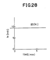
- FIG.28 shows the result of experiment conducted on the integrated circuit of FIG.26 under a same condition as in the case of FIG.10B.
- the small dip of the drain current occurring in the case of FIG.10B as a result of the side gate effect it entirely eliminated in the structure of FIG.26 and thus, the integrated circuit of the present embodiment is entirely free from the side gate effect.
- FIG.29 shows an eleventh embodiment of the present invention.
- these parts that are already described with reference to the preceding drawings are given identical reference numerals and the description thereof will be omitted.
- the AlGaAs layer 26a of the structure of FIG.26 is omitted and thus, there is only one AlGaAs layer 26b adjacent to the insulating GaAs buffer layer 26 at the upper side thereof.
- the hot electrons that are entering from the buffer layer 28 into the buffer layer 26 are effectively blocked by the layer 26b and the side gate effect is successfully eliminated.
Landscapes
- Junction Field-Effect Transistors (AREA)
Applications Claiming Priority (4)
| Application Number | Priority Date | Filing Date | Title |
|---|---|---|---|
| JP1302667A JP2963120B2 (ja) | 1989-11-21 | 1989-11-21 | 半導体装置及びその製造方法 |
| JP302667/89 | 1989-11-21 | ||
| JP19909390A JP2949518B2 (ja) | 1990-07-30 | 1990-07-30 | 半導体装置及びその製造方法 |
| JP199093/90 | 1990-07-30 |
Publications (3)
| Publication Number | Publication Date |
|---|---|
| EP0437702A2 true EP0437702A2 (de) | 1991-07-24 |
| EP0437702A3 EP0437702A3 (en) | 1993-01-07 |
| EP0437702B1 EP0437702B1 (de) | 1998-08-12 |
Family
ID=26511336
Family Applications (1)
| Application Number | Title | Priority Date | Filing Date |
|---|---|---|---|
| EP90122207A Expired - Lifetime EP0437702B1 (de) | 1989-11-21 | 1990-11-20 | Integrierte Halbleiterschaltung mit Isolationszonen zwischen Komponenten aus Verbindungshalbleitern und Methode zu deren Herstellung |
Country Status (1)
| Country | Link |
|---|---|
| EP (1) | EP0437702B1 (de) |
Cited By (3)
| Publication number | Priority date | Publication date | Assignee | Title |
|---|---|---|---|---|
| EP0591607A3 (en) * | 1992-08-11 | 1997-01-08 | Mitsubishi Electric Corp | Isolated semiconductor device and production method thereof |
| EP0744773A3 (de) * | 1995-05-25 | 1997-12-29 | Murata Manufacturing Co., Ltd. | Halbleiterbauelement mit plasmabehandelter Schicht und Herstellungsverfahren |
| CN112464154A (zh) * | 2020-11-27 | 2021-03-09 | 中国船舶重工集团公司第七0四研究所 | 一种基于无监督学习的自动筛选有效特征的方法 |
Family Cites Families (2)
| Publication number | Priority date | Publication date | Assignee | Title |
|---|---|---|---|---|
| JPS61107758A (ja) * | 1984-10-31 | 1986-05-26 | Fujitsu Ltd | GaAs集積回路及びその製造方法 |
| JPS61256675A (ja) * | 1985-05-09 | 1986-11-14 | Sumitomo Electric Ind Ltd | シヨツトキゲ−ト電界効果トランジスタの製造方法 |
-
1990
- 1990-11-20 EP EP90122207A patent/EP0437702B1/de not_active Expired - Lifetime
Cited By (5)
| Publication number | Priority date | Publication date | Assignee | Title |
|---|---|---|---|---|
| EP0591607A3 (en) * | 1992-08-11 | 1997-01-08 | Mitsubishi Electric Corp | Isolated semiconductor device and production method thereof |
| EP0744773A3 (de) * | 1995-05-25 | 1997-12-29 | Murata Manufacturing Co., Ltd. | Halbleiterbauelement mit plasmabehandelter Schicht und Herstellungsverfahren |
| KR100238533B1 (ko) * | 1995-05-25 | 2000-01-15 | 무라타 야스타카 | 플라즈마-처리층을 가진 반도체 장치 및 이의 제조 방법 |
| US6458675B1 (en) | 1995-05-25 | 2002-10-01 | Murata Manufacturing Co., Ltd. | Semiconductor device having a plasma-processed layer and method of manufacturing the same |
| CN112464154A (zh) * | 2020-11-27 | 2021-03-09 | 中国船舶重工集团公司第七0四研究所 | 一种基于无监督学习的自动筛选有效特征的方法 |
Also Published As
| Publication number | Publication date |
|---|---|
| EP0437702B1 (de) | 1998-08-12 |
| EP0437702A3 (en) | 1993-01-07 |
Similar Documents
| Publication | Publication Date | Title |
|---|---|---|
| US4452646A (en) | Method of making planar III-V compound device by ion implantation | |
| US5001536A (en) | Semiconductor device | |
| US20110042719A1 (en) | Semiconductor device and method of manufacturing a semiconductor device | |
| US5866925A (en) | Gallium nitride junction field-effect transistor | |
| US5420059A (en) | Method of making a high performance MESFET with multiple quantum wells | |
| EP0555886A2 (de) | Heteroübergang-Feld-Effekt-Transistor | |
| US5276340A (en) | Semiconductor integrated circuit having a reduced side gate effect | |
| JPS62189762A (ja) | 3−5族化合物基体上に半導体装置を製造する方法 | |
| EP0151309B1 (de) | Feldeffecttransistor mit hoher Elektronenbeweglichkeit | |
| KR920003799B1 (ko) | 반도체 장치 | |
| KR910002818B1 (ko) | Mes fet의 제조방법 | |
| US4717685A (en) | Method for producing a metal semiconductor field effect transistor | |
| EP0080714B1 (de) | Halbleiteranordnung mit Heteroübergängen | |
| US4710787A (en) | Semiconductor device | |
| KR100329251B1 (ko) | 반도체소자및그제조방법 | |
| US5493136A (en) | Field effect transistor and method of manufacturing the same | |
| US5101245A (en) | Field effect transistor and method for making same | |
| US5296390A (en) | Method for fabricating a semiconductor device having a vertical channel of carriers | |
| EP0437702B1 (de) | Integrierte Halbleiterschaltung mit Isolationszonen zwischen Komponenten aus Verbindungshalbleitern und Methode zu deren Herstellung | |
| EP0130774B1 (de) | Verfahren zum Herstellen bipolarer Transistoren | |
| US5053846A (en) | Semiconductor bipolar device with phosphorus doping | |
| EP0469768A1 (de) | Ein im wesentlichen linearer Feldeffekttransistor und dessen Herstellungsverfahren | |
| KR910006698B1 (ko) | 반도체 장치 | |
| GB2239557A (en) | High electron mobility transistors | |
| US5413947A (en) | Method for manufacturing a semiconductor device with an epitaxial void |
Legal Events
| Date | Code | Title | Description |
|---|---|---|---|
| PUAI | Public reference made under article 153(3) epc to a published international application that has entered the european phase |
Free format text: ORIGINAL CODE: 0009012 |
|
| AK | Designated contracting states |
Kind code of ref document: A2 Designated state(s): DE FR GB |
|
| PUAL | Search report despatched |
Free format text: ORIGINAL CODE: 0009013 |
|
| AK | Designated contracting states |
Kind code of ref document: A3 Designated state(s): DE FR GB |
|
| 17P | Request for examination filed |
Effective date: 19930208 |
|
| 17Q | First examination report despatched |
Effective date: 19940620 |
|
| GRAG | Despatch of communication of intention to grant |
Free format text: ORIGINAL CODE: EPIDOS AGRA |
|
| GRAG | Despatch of communication of intention to grant |
Free format text: ORIGINAL CODE: EPIDOS AGRA |
|
| GRAH | Despatch of communication of intention to grant a patent |
Free format text: ORIGINAL CODE: EPIDOS IGRA |
|
| RBV | Designated contracting states (corrected) |
Designated state(s): FR |
|
| REG | Reference to a national code |
Ref country code: DE Ref legal event code: 8566 |
|
| GRAH | Despatch of communication of intention to grant a patent |
Free format text: ORIGINAL CODE: EPIDOS IGRA |
|
| GRAA | (expected) grant |
Free format text: ORIGINAL CODE: 0009210 |
|
| AK | Designated contracting states |
Kind code of ref document: B1 Designated state(s): FR |
|
| ET | Fr: translation filed | ||
| PLBE | No opposition filed within time limit |
Free format text: ORIGINAL CODE: 0009261 |
|
| STAA | Information on the status of an ep patent application or granted ep patent |
Free format text: STATUS: NO OPPOSITION FILED WITHIN TIME LIMIT |
|
| 26N | No opposition filed | ||
| PGFP | Annual fee paid to national office [announced via postgrant information from national office to epo] |
Ref country code: FR Payment date: 20071108 Year of fee payment: 18 |
|
| REG | Reference to a national code |
Ref country code: FR Ref legal event code: ST Effective date: 20090731 |
|
| PG25 | Lapsed in a contracting state [announced via postgrant information from national office to epo] |
Ref country code: FR Free format text: LAPSE BECAUSE OF NON-PAYMENT OF DUE FEES Effective date: 20081130 |