EP0437740B1 - Integriertes, optoelektronisches, bistabiles Kippglied - Google Patents
Integriertes, optoelektronisches, bistabiles Kippglied Download PDFInfo
- Publication number
- EP0437740B1 EP0437740B1 EP90124047A EP90124047A EP0437740B1 EP 0437740 B1 EP0437740 B1 EP 0437740B1 EP 90124047 A EP90124047 A EP 90124047A EP 90124047 A EP90124047 A EP 90124047A EP 0437740 B1 EP0437740 B1 EP 0437740B1
- Authority
- EP
- European Patent Office
- Prior art keywords
- optical
- transistor
- clock generator
- high speed
- coupled
- Prior art date
- Legal status (The legal status is an assumption and is not a legal conclusion. Google has not performed a legal analysis and makes no representation as to the accuracy of the status listed.)
- Expired - Lifetime
Links
- 230000005693 optoelectronics Effects 0.000 title description 5
- 230000003287 optical effect Effects 0.000 claims description 97
- 239000000463 material Substances 0.000 claims description 15
- 230000008878 coupling Effects 0.000 claims description 14
- 238000010168 coupling process Methods 0.000 claims description 14
- 238000005859 coupling reaction Methods 0.000 claims description 14
- 239000004065 semiconductor Substances 0.000 claims description 14
- 239000000835 fiber Substances 0.000 claims description 13
- 239000000758 substrate Substances 0.000 claims description 12
- 230000005540 biological transmission Effects 0.000 claims description 10
- 230000005855 radiation Effects 0.000 claims description 9
- 239000002800 charge carrier Substances 0.000 claims description 8
- 239000010703 silicon Substances 0.000 claims description 6
- 229910052710 silicon Inorganic materials 0.000 claims description 6
- 230000006870 function Effects 0.000 claims description 5
- 239000011248 coating agent Substances 0.000 claims description 4
- 238000000576 coating method Methods 0.000 claims description 4
- 229910052732 germanium Inorganic materials 0.000 claims description 2
- GNPVGFCGXDBREM-UHFFFAOYSA-N germanium atom Chemical compound [Ge] GNPVGFCGXDBREM-UHFFFAOYSA-N 0.000 claims description 2
- 230000005669 field effect Effects 0.000 claims 6
- 230000003111 delayed effect Effects 0.000 claims 1
- 229910001218 Gallium arsenide Inorganic materials 0.000 description 11
- 239000013307 optical fiber Substances 0.000 description 8
- 238000010586 diagram Methods 0.000 description 7
- 230000002123 temporal effect Effects 0.000 description 5
- XUIMIQQOPSSXEZ-UHFFFAOYSA-N Silicon Chemical compound [Si] XUIMIQQOPSSXEZ-UHFFFAOYSA-N 0.000 description 4
- 238000005516 engineering process Methods 0.000 description 4
- 230000004044 response Effects 0.000 description 4
- 229910000980 Aluminium gallium arsenide Inorganic materials 0.000 description 3
- 230000008901 benefit Effects 0.000 description 3
- 230000015556 catabolic process Effects 0.000 description 3
- 238000004891 communication Methods 0.000 description 3
- 238000006731 degradation reaction Methods 0.000 description 3
- 230000000694 effects Effects 0.000 description 3
- 238000000034 method Methods 0.000 description 3
- 238000005286 illumination Methods 0.000 description 2
- 230000001939 inductive effect Effects 0.000 description 2
- 238000012545 processing Methods 0.000 description 2
- 230000009467 reduction Effects 0.000 description 2
- 230000006978 adaptation Effects 0.000 description 1
- 230000003321 amplification Effects 0.000 description 1
- 238000013459 approach Methods 0.000 description 1
- 230000001427 coherent effect Effects 0.000 description 1
- 230000000295 complement effect Effects 0.000 description 1
- 230000006835 compression Effects 0.000 description 1
- 238000007906 compression Methods 0.000 description 1
- 230000003750 conditioning effect Effects 0.000 description 1
- 239000004020 conductor Substances 0.000 description 1
- 238000010276 construction Methods 0.000 description 1
- 230000002939 deleterious effect Effects 0.000 description 1
- 230000001419 dependent effect Effects 0.000 description 1
- 230000001627 detrimental effect Effects 0.000 description 1
- 238000011982 device technology Methods 0.000 description 1
- 230000001747 exhibiting effect Effects 0.000 description 1
- 238000003384 imaging method Methods 0.000 description 1
- 230000010354 integration Effects 0.000 description 1
- 239000002184 metal Substances 0.000 description 1
- 238000003199 nucleic acid amplification method Methods 0.000 description 1
- 230000035945 sensitivity Effects 0.000 description 1
- 230000008054 signal transmission Effects 0.000 description 1
- 239000007787 solid Substances 0.000 description 1
- 230000000638 stimulation Effects 0.000 description 1
- 230000001131 transforming effect Effects 0.000 description 1
- 230000001052 transient effect Effects 0.000 description 1
Images



Classifications
-
- H—ELECTRICITY
- H03—ELECTRONIC CIRCUITRY
- H03K—PULSE TECHNIQUE
- H03K3/00—Circuits for generating electric pulses; Monostable, bistable or multistable circuits
- H03K3/02—Generators characterised by the type of circuit or by the means used for producing pulses
- H03K3/027—Generators characterised by the type of circuit or by the means used for producing pulses by the use of logic circuits, with internal or external positive feedback
- H03K3/037—Bistable circuits
-
- H—ELECTRICITY
- H03—ELECTRONIC CIRCUITRY
- H03K—PULSE TECHNIQUE
- H03K3/00—Circuits for generating electric pulses; Monostable, bistable or multistable circuits
- H03K3/02—Generators characterised by the type of circuit or by the means used for producing pulses
- H03K3/353—Generators characterised by the type of circuit or by the means used for producing pulses by the use, as active elements, of field-effect transistors with internal or external positive feedback
- H03K3/356—Bistable circuits
-
- H—ELECTRICITY
- H03—ELECTRONIC CIRCUITRY
- H03K—PULSE TECHNIQUE
- H03K3/00—Circuits for generating electric pulses; Monostable, bistable or multistable circuits
- H03K3/02—Generators characterised by the type of circuit or by the means used for producing pulses
- H03K3/42—Generators characterised by the type of circuit or by the means used for producing pulses by the use, as active elements, of opto-electronic devices, i.e. light-emitting and photoelectric devices electrically- or optically-coupled
Definitions
- This invention relates generally to optoelectronic devices and, in particular, to a high-speed, low-jitter toggle Flip-Flop (F/F) device coupled to an optical pulse source for converting an optical pulse into electrical signals.
- F/F Flip-Flop
- the electrical transmission of fast timing signals introduces timing skew problems resulting from the limited bandwidth associated with the transmission and reception of the electrical signals through conventional electrical cables and transmission lines.
- One especially deleterious effect of the limited bandwidth is a degradation of fast risetime pulses.
- a variation in pulse receiver sensitivity or threshold causes an uncertainty or jitter as to an actual time of the arrival of electrical pulse. If the electrical pulse is being employed as a timing signal in, for example, a high-speed data processing system the presence of pulse jitter is especially detrimental.
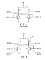
- Fig. 1 illustrates a simplified diagram of a conventional toggle circuit constructed as a set-reset flip-flop (SR F/F).
- the SR F/F includes two transistors Q A and Q B interconnected in a cross-coupled manner as shown. Each transistor is further coupled to a source of operating power (V dd ) through an associated load resistance R A and R B .
- V dd source of operating power
- INPUT A sets OUTPUT logically HIGH
- an electrical pulse to INPUT B resets the OUTPUT logically LOW.
- the complementary signal OUTPUT ⁇ is LOW when OUTPUT is HIGH and vice versa.
- SR F/F circuit One advantage of such a SR F/F circuit is that the output is always in a known logical state, as is important in the clocking of a computer system. That is, the OUTPUT signal may be employed as a clocking signal for logic circuitry of a computer system.
- One proposed solution to this problem involves transmitting the input pulses as an optical signal instead of an electrical signal. For example, due to the inherently much wider bandwidth of an optical fiber the transmission of a fast rise time optical pulse through the fiber occurs without significant signal degradation.
- optoelectronic circuits generally include electrical switching circuitry coupled to an optical receiver.
- the receiver typically includes a photosensor followed by several gain stages with output of the gain stages being applied to the associated switching circuitry.
- a problem with this conventional arrangement relates to the propagation delay between a time light is incident upon the photosensor and a time at which the switching circuit responds by changing state.
- Another problem relates to temporal jitter resulting from uncertainty in the propagation delay produced by the gain stages proceeding the logic circuitry.
- Brojdo teaches a semiconductor memory array using a pair of bipolar transistors arranged as a F/F wherein a base of each transistor is connected to a high impedance when a power supply voltage is removed. As the high impedance forces slow decay of charge stored in the transistors, the state of the F/F can be maintained by a pulsed power supply, thereby reducing the average power dissipation of the F/F.
- the memory can be written optically by photogenerating charge in the base of one of the transistors, thereby unbalancing the transistors.
- a laser is employed to address a hologram for providing a desired light pattern for illuminating the memory array.
- This device specifically uses the low speed nature of the high impedance circuits to integrate the optical signals being applied.
- a F/F circuit configuration is used the application and nature of operation do not address the problem converting optical pulses into fast rise-time, low jitter electrical logic signals.
- a fiber-optic flip-flop receiver of the present type is known from IBM Technical Disclosure Bulletin Vol 25 No 7B Dec 82. pp 3887-3888.
- U.S. Paten No ts are noted of being of general interest.
- U.S. Patent 4,223,330 entitled “Solid-State Imaging Device” describes a solid-state image pickup device for use in a TV camera and the like.
- U.S. Patent 4,295,058, entitled “Radiant Energy Activated Semiconductor Switch” describes various power switching circuits using a light sensor such as photodiode coupled to a gate of a depletion-mode FET.
- U.S. Patent 4,390,790 entitled “Solid State Optically Coupled Electrical Power Switch” relates to optically isolated switching devices such as solid-state relays for power switching or analog switches for signal switching.
- U.S. Patent 4,223,330 entitled “Solid-State Imaging Device” describes a solid-state image pickup device for use in a TV camera and the like.
- U.S. Patent 4,295,058, entitled “Radiant Energy Activated Semiconductor Switch” describes various power switching circuits using a light sensor such
- Patent 4,521,888 entitled “Semiconductor Device Integrating a Laser and a Transistor”
- U.S. Patent 4,739,306 entitled “Calibrated-Weight Balance and an Analog-to-Digital Converter in which the Balance is Employed”
- ADC Analog-to-Digital Converter
- the circuit includes a multivibrator comprising cross- coupled FETs 15 and 16.
- this patent does not disclose the provision of optical inputs for driving the multivibrator.
- Optical switched flip flops are also known from EP- A- 0 345 494 and US- A- 3 624 419.
- the EP- A- 345 494 discloses a memory cell comprising a pair of cross-coupled switching means fabricated on a substrate and means for receiving pulses of optical radiation integrally formed on the substrate with each of the switching means comprising a first optical receiver and a second optical receiver, each being coupled to an input of an associated one of the switching means for causing the switching means to alternately toggle between an on state and an off state.
- each of the switching means comprising a first optical receiver and a second optical receiver, each being coupled to an input of an associated one of the switching means for causing the switching means to alternately toggle between an on state and an off state.
- one of these memory cells can be advantageously used to create a low jitter toggle device for transforming optical pulses to electrical pulses.
- Those memory cells are usually optical written and read out.
- the problem of the invention is, to provide an optoelectronic pulse converter for converting an optical pulse into an electrical pulse having a fast risetime and a minimum of timing uncertainty.
- the invention also meets the following objects:
- Timing generation circuit that provides for the transmission of optical pulses of ultrafast risetime through extremely high- bandwidth optical fibers and which further converts these optical pulses into an electrical timing signal having leading and trailing edges exhibiting minimal timing uncertainty.
- a further object of the invention is met in providing clock generation circuitry for a high-speed, short cycle time data processor that employs the transmission of optical clock synchronization pulses of ultrafast risetime through extremely high- bandwidth optical fibers and which further converts these optical pulses into an electrical clock signal having a minimum pulse skew.
- the device according to the invention operates as a pulse converter and converts optical pulses to electrical pulses.
- the pulse converter includes a set-reset flip/flop, or OPTOGLE, having a pair of cross-coupled switching devices such as transistors or logic gates.
- the converter operates by coupling pulses of optical radiation to each of the switching devices for causing the switching devices to alternately toggle between an on-state and an off-state.
- Optical inputting devices such as photodiodes or photoconductors, or the gates of FET transistors themselves, are integrally formed upon a common substrate with the switching devices for minimizing stray inductive and capacitive reactances to substantially eliminate temporal jitter in an electrical output signal.
- a pulsed laser source and a fiber optic or optical waveguide provide non-overlapping optical pulses to each of the switching devices.
- each of the switching devices is a GaAs MESFET device having a gate terminal comprised of a substantially transparent layer of electrical conductor having an interdigitated geometry and an overlying anti-reflection (AR) coating.
- a gate terminal comprised of a substantially transparent layer of electrical conductor having an interdigitated geometry and an overlying anti-reflection (AR) coating.
- AR anti-reflection
- the transistors are each constructed of a semiconductor material having a characteristic energy bandgap for absorbing the optical pulse and generating sufficient charge carriers therefrom to induce a current flow though the transistor.
- the semiconductor material may be comprised of Group III-V material, of silicon, of other Group IV materials such as germanium or of combinations of these materials.
- OPTOGLE 10 is constructed in some respects in a similar manner to the circuit of Fig. 1.
- OPTOGLE 10 includes two transistors Q 1 and Q 2 having their respective gate terminals interconnected in a cross-coupled manner as shown. Each transistor further has a drain terminal coupled to a source of operating power (V dd ) through an associated load, such as a resistance R 1 and R 2 , and a source terminal coupled to a common potential.
- V dd source of operating power
- R 1 and R 2 a resistance
- the transistors are MESFET devices comprised of semiconductor material having a high electron mobility, such as GaAs.
- a region between the source and drain of each MESFET is illuminated with a light pulse of narrow pulse width to achieve a high frequency of operation.
- the source of the light is a laser source such as a mode-locked gas laser, a mode-locked solid-state laser, or a gain-switched semiconductor diode laser as disclosed in the aforementioned European Patent Application EP 90 107 579.6.
- the MESFETs Due to the nature of the optical input, the MESFETs have an equivalent fourth port that is highly isolated from the gate, drain and source terminals. This equivalent fourth port is shown schematically in Fig. 2 and is referred to as OPTICAL INPUT A and OPTICAL INPUT B.
- the incident photon energy is greater than the semiconductor bandgap, a large density of charge carriers is generated.
- These charge carriers produce fast electrical pulses between the drain and source terminals of the FET by means of photoconductivity.
- the optical pulsewidth is preferably much shorter than the charge carrier lifetime, this effect is transient.
- a risetime of the photoconductive signal is approximately the same as a risetime of the optical pulse while the fall time of the photoconductive signal is a function of the charge carrier lifetime.
- the photoconductive gain defined as the number of charge carriers crossing a sample per second divided by the number of photons absorbed per second, is approximately the ratio of optical pulse duration to the transit time of the charge. As a result a large gain may be realized.
- the light-induced electrical pulse controls the output state of the OPTOGLE 10 in substantially the same manner as the electrical inputs INPUT A and INPUT B, and may be used interchangeably if desired. It should be noted that both electrical and optical inhibit capability is implicit in the circuit in that toggle activity can be inhibited by the application of a long duration pulse, or level, through either the electrical or the optical inputs. In general the transistor gates serve several purposes including providing positive feedback during changes of state and also providing external electrical terminals.
- an optical pulse applied to OPTICAL INPUT A sets OUTPUT logically HIGH, while an optical pulse applied to OPTICAL INPUT B resets the OUTPUT logically LOW.
- electrical pulses could be substituted for some of the optical pulses or could be used to inhibit the operation of the optical pulses.
- the optical pulses may be derived from separate sources or from a common source. If the latter approach is employed one of the pulses is passed through an optical delay device, such as longer path length optical fiber, so that the second pulse is temporally offset from the first pulse by a desired amount. The amount of temporal offset affects the output electrical signal duty cycle as shown.
- One significant advantage of directly coupling the light pulse to the gates of the transistors of the OPTOGLE 10 is the resulting simplicity of the circuit. That is, the MESFET itself functions as a photosensor and, with no signal amplifying or conditioning stage(s) required as with conventional types of optoelectronic devices, the propagation delay and the temporal jitter is minimized. Thus, the OPTOGLE 10 significantly reduces pulse skew characteristics which are especially critical in data processing clock signal distribution.
- Fig. 3 illustrates an enlarged view of a portion of an interdigitated MESFET.
- the gate electrode 12a is disposed between the source electrode 12b and the drain electrode 12c.
- An illuminating laser beam spot 14 has a diameter of approximately 30 microns.
- the interdigitated geometry of the gate electrode 12a beneficially reduces shadow effects of the electrodes, thus improving light coupling, while also providing for a low interelectrode capacitance.
- the provision of an anti-reflection (AR)-coating 18 over the gate electrode 12a further improves light coupling efficiency, the AR coating being optimized for the wavelength of the incident optical radiation.
- AR anti-reflection
- Coupling efficiency may be further improved with transistor gates constructed of semitransparent electrodes such as electrodes comprised of a relatively thin layer of metal having a thickness of approximately 10 nanometers.
- transistor gates constructed of semitransparent electrodes such as electrodes comprised of a relatively thin layer of metal having a thickness of approximately 10 nanometers.
- the MESFETs Q1 and Q2, associated electrodes 12a, 12b, 12c and other components are formed on a common substrate 16.
- the characteristics of the GaAs OPTOGLE 10 were determined with the experimental apparatus 20 schematically shown in Fig. 4.
- the apparatus 20 includes a pair of optical fibers 22a and 22b each of which conveys light from an associated source 24a and 24b.
- Sources 24a and 24b are preferably each a coherent source.
- An output end of each the fibers 22 is coupled to a collimating lens 26 from which the light energy is relayed to a dichroic mirror 28.
- a focusing lens 30 Optically coupled to one side of the dichroic mirror 28 is a focusing lens 30 for focusing the outputs of the sources 24 onto respective gate electrodes of an integrated circuit device 32 containing the OPTOGLE 10.
- Optically coupled to the opposite side of the dichroic mirror 28 is a beamsplitter 34.
- An illuminator 36 for camera 40 provides illumination through a collimating lens 38. Camera 40 views the scene through a focusing lens 42. This arrangement permits the optical stimulation of the OPTOGLE 10 and the
- Fig. 5 illustrates the OUTPUT signal of the OPTOGLE 10. Each time division along the x-axis represents 500 picoseconds.
- the input pulse is the input electrical pulse applied to a laser diode source in order to generate the optical pulse that was applied to the OPTOGLE 10.
- Suitable sources of radiation include mode-locked Nd:Yag lasers, Nd:YLF lasers, AlGaAs any source capable of generating ultrashort, fast risetime, high-peak-power optical pulses at a high repetition rate.
- the wavelength of the pulse is preferably within a range of wavelengths strongly absorbed by the semiconductor material.
- both GaAs and silicon strongly absorb visible and near-infrared radiation.
- With known types of optical pulse compression techniques using optical fibers and gratings a duration of the optical pulses can be reduced to the subpicosecond range.
- the GaAs MESFET-based OPTOGLE 10 although not entirely optimized for such operation, has been found to require a pulse energy of 4 pJoules.
- a mode-locked laser with average output power of 1 Watt has sufficient power to simultaneously address approximately 500 of the OPTOGLE pulse converters.
- the gate electrodes of two MESFET devices were illuminated with laser beam pulses having an approximately 30 micron spot size.
- the light pulses were produced by injecting a train of 250 picosecond electrical pulses into an AlGaAs diode laser having a nominal wavelength of 780 nanometers.
- the optical pulses were provided through fiber optics as depicted in Fig. 4.
- Fig. 8a shows a FET flip-flop with photodiode inputs.
- a circuit of this type is known from US-A-3 624 419.
- the photodiodes D1 and D2 are integrated into the same substrate as the FETs Q1 and Q2 and the other components of the SR F/F.
- One important advantage of this technique is the reduction of required circuit dimensions with a corresponding reduction of stray circuit reactances, both capacitive and inductive, at the photosensor leads. As a result optical input pulses are efficiently received and circuit speeds are very fast.
- any of the SR F/F embodiments may implemented with bipolar transistor technology, instead of the FET technology shown.
- the SR F/F may be implemented by more general logic devices, such as the NOR gates (G1 and G2) shown in Fig. 9.
- This embodiment also includes integrally formed photodiodes D1 and D2 and is implemented as an integrated photosensor/logic circuit combination to achieve fast switching times.
- photovoltaic optical sensors such as the photodiodes D1 and D2 may be replaced, as in Fig. 8b, by integrated photoconductive sensors (S1 and S2).
- integrated photoconductive sensors S1 and S2
- Such devices such as those constructed of Group III-V, silicon and other materials exhibit very fast (picosecond) response times and are well suited for this use.
- an important aspect is the integration of the photosensor devices with the cross-coupled switching circuitry, with no additional amplifier circuits being required or deployed, thereby significantly reducing temporal jitter in the output pulse stream.
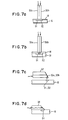
- the optical pulses may be applied, as depicted in Figs. 7a-7d, through optical fibers 50a and 50b having flat, polished ends (Fig. 7a) or integral focusing optics (Fig. 7b).
- the fiber 50a and 50b ends are bonded or otherwise fixedly coupled to the appropriate electrode region of each of the transistors Q1 and Q2 or to the associated one of the photodiodes D1 or D2 or photoconductors S1 or S2.
- Fig. 7c illustrates the fibers 50a and 50b having a beveled end and coupled to a v-block.
- Fig. 7d illustrates an optical waveguide 54 fabricated upon the substrate 16 and having an end in optical communication with the SR F/F for coupling optical pulses thereto. It is also within the scope of the invention to convey the optical radiation to the transistors by integrating, for example, a plurality of AlGaAs laser devices onto an integrated circuit device with the OPTOGLE 10.
- OPTOGLEs may be constructed with silicon FET technology although such devices exhibit a slower response due to relatively lower carrier mobility than similar devices constructed with GaAs and/or other Group III-V materials such as InP.
- electron mobility is approximately 8600cm 2 /Vs and electron transit time is approximately 15 picoseconds for an electrode 12 spacing of five microns and an applied voltage of two volts.
- the gain is approximately 10 for laser pulses of 150 picoseconds in duration. Modulation of the gate 12a voltage during operation also results in a current amplification.
Landscapes
- Electronic Switches (AREA)
- Light Receiving Elements (AREA)
- Solid State Image Pick-Up Elements (AREA)
Claims (14)
- Ein schneller Taktgenerator zu Übertragungszwecken, um optische Signale an logische Schaltkreise anzupassen: mit:einem Schaltkreis (10), wie er von Speicherzellen bekannt ist, um optische Impulse in elektrische Impulse umzuwandeln,wobei der Schaltkreis (10) ein Paar kreuzgekoppelter Schaltmittel enthält, die auf einem Substrat (16) hergestellt wurden, und Empfangsmittel, um Impulse von optischer Strahlung zu empfangen, die vollständig auf dem Substrat (16) aufgebaut wird, wobei jedes der Schaltmittel einen ersten optischen Empfänger (D1, Q1) und einen zweiten optischen Empfänger (D2, Q2) enthält, von denen jeder über einen Eingang mit einem der angeschlossenen Schaltmittel verbunden ist, um die Schaltmittel zu veranlassen, abwechselnd zwischen einem Ein- und einem Ausstatus hinund herzuschalten,wobei der Taktgenerator außerdem faseroptische (50a, 50b) und/oder optische Wellenleitermittel (54) enthält, um die optischen Impulse mit den Empfangsmitteln zu koppeln, wobei diese Empfangsmittel ein MESFET enthalten, um das Licht zu empfangen und der MESFET einen Gate-Anschluß (12a) mit einer fingerartig ineinandergreifenden Geometrie hat, um die Lichtkopplung zu verbessern,und einen Ausgangsanschluß (Ausgang) bei einem der Schaltmittel, um die umgewandelten elektrischen Impulse bereitzustellen.
- Ein schneller Taktgenerator gemäß Anspruch 1, der dadurch gekennzeichnet ist, daß
der optische Impuls mit dem ersten optischen Empfänger (D1, Q1) gekoppelt ist und von einer optischen Verzögerungseinrichtung verzögert wird, bevor dieser auch mit dem zweiten optischen Empfänger (D2, Q2) verbunden wird. - Ein schneller Taktgenerator gemäß Anspruch 1 oder 2, dadurch gekennzeichnet, daß
die Lichtwellenleiter (50a, 50b) dazu dienen, um den optischen Impuls mit den Empfangsmitteln zu koppeln, wobei die Lichtwellenleiter (50a, 50b) ein abgeschrägtes Ende haben und über einen V-förmigen Block mit dem Substrat verbunden sind. - Ein schneller Taktgenerator gemäß Anspruch 1 oder 2, dadurch gekennzeichnet, daß
die Lichtwellenleiter (50a, 50b) dazu dienen, um den optischen Impuls mit den Empfangsmitteln zu verbinden, wobei die Lichtwellenleiter (50a, 50b) flache polierte Enden oder eine eingebaute Fokussierungsoptik haben. - Ein schneller Taktgenerator gemäß Anspruch 4, dadurch gekennzeichnet, daß
die Lichtwellenleiter (50a, 50b) mit den ersten und zweiten optischen Empfängern (D1, D2, Q1, Q2) in den Empfangsmitteln verbunden sind. - Ein schneller Taktgenerator gemäß Anspruch 1 oder 2, dadurch gekennzeichnet, daß
die Empfangsmittel mit einer impulsgesteuerten Laserquelle über ein eingreifendes Wellenleitermittel (54) gekoppelt sind, das vollständig auf dem Substrat (16) aufgebaut ist. - Ein schneller Taktgenerator gemäß irgendeinem der Ansprüche 1 bis 6, dadurch gekennzeichnet, daß
die Schaltmittel einen Transistor (Q1, Q2) enthalten, der aus einem Halbleitermaterial hergestellt wird und einen typischen Bandabstand hat, um den optischen Impuls zu absorbieren und daraus ausreichende Ladungsträger zu generieren, um einen Stromfluß durch den Transistor einzuleiten. - Ein schneller Taktgenerator gemäß irgendeinem der Ansprüche 1 bis 7 dadurch gekennzeichnet, daß
das Substrat (16) ein Halbleitermaterial ist, das aus der Gruppe mit III-V Material und Silikon ausgewählt wurde. - Ein schneller Taktgenerator gemäß irgendeinem der Ansprüche 1 bis 8, dadurch gekennzeichnet, daß
das Schaltmittel ein Feldeffekttransistor ist (Q1, Q2), der aus einem Halbleitermaterial hergestellt wird, mit einem typischen Energiebandabstand, um den optischen Impuls zu absorbieren und ausreichende Ladungsträger zu generieren, um den Stromfluß durch den Feldeffekttransistor (Q1, Q2) einzuleiten, und wobei die Empfangsmittel einen Gate-Anschlußbereich des Feldeffekttransistors (Q1, Q2) bereitstellen. - Ein schneller Taktgenerator gemäß Anspruch 9, dadurch gekennzeichnet, daß
der Gate-Anschluß (12a) neben einer Antireflexschicht angeordnet ist (18). - Ein schneller Taktgenerator gemäß irgendeinem der Ansprüche 1 bis 8, dadurch gekennzeichnet, daß
das Schaltmittel eine Feldeffekttransistoreinheit (Q1, Q2) enthält, wobei das Empfangsmittel ein fotovoltaisches und ein fotoleitendes Gerät (D1, D2, S1, S2) enthält, das mit einem Gate-Anschluß der Feldeffekttransistoreinheit (Q1, Q2) gekoppelt ist. - Ein schneller Taktgenerator gemäß irgendeinem der Ansprüche 1 bis 8, dadurch gekennzeichnet, daß
das Schaltmittel ein logisches Element (G1, G2) enthält, vorzugsweise mit mindestens zwei Eingängen und das entsprechend einer NOR-Funktion arbeitet. - Ein schneller Taktgenerator gemäß den Ansprüchen 1 bis 12, gekennzeichnet durch,erste und zweite Transistormittel (Q1, Q2), von denen jedes einen Ausgangsanschluß hat, der mit einer angeschlossenen Last (R1, R2) und einem Steueranschluß gekoppelt ist, wobei die ersten und zweiten Transistormittel kreuzgekoppelt sind, so daß der Steueranschluß von einem der Transistormittel mit dem Ausgangsanschluß des anderen Transistormittels verbunden ist, wobei das erste und zweite Transistormittel auf einem gemeinsamen Substrat hergestellt wurden undMittel, um die Impulse der optischen Strahlung in den Steueranschluß des ersten Transistormittels einzugeben, und um die Impulse der optischen Strahlung in den Steueranschluß des zweiten Transistormittels (Q2) einzugeben, wobei das Eingangsmittel eine erste Fotodiode (D1) oder einen Fotoleiter (S1) enthält, die bzw. der mit dem Steueranschluß des ersten Transistormittels (Q1) gekoppelt ist, und eine zweite Fotodiode (D2) oder einen Fotoleiter (S2), die bzw. der mit dem Steueranschluß des zweiten Transistormittels (Q2) gekoppelt ist, und wobei die Eingangsmittel außerdem aus mindestens einem Teil des Steueranschlusses von sowohl dem ersten als auch dem zweiten Transistormittel bestehen.
- Ein schneller Taktgenerator gemäß irgendeinem der Ansprüche 1 bis 13, dadurch gekennzeichnet, daß
die Schaltmittel jeweils einen bipolaren Transistor enthalten oder einen Feldeffekttransistor, der aus Silikon, Germanium, Material der Gruppe III-V oder aus Kombinationen daraus besteht.
Applications Claiming Priority (2)
| Application Number | Priority Date | Filing Date | Title |
|---|---|---|---|
| US466902 | 1990-01-18 | ||
| US07/466,902 US5045680A (en) | 1990-01-18 | 1990-01-18 | Integrated circuit optoelectronic toggle F/F |
Publications (2)
| Publication Number | Publication Date |
|---|---|
| EP0437740A1 EP0437740A1 (de) | 1991-07-24 |
| EP0437740B1 true EP0437740B1 (de) | 1997-10-29 |
Family
ID=23853525
Family Applications (1)
| Application Number | Title | Priority Date | Filing Date |
|---|---|---|---|
| EP90124047A Expired - Lifetime EP0437740B1 (de) | 1990-01-18 | 1990-12-13 | Integriertes, optoelektronisches, bistabiles Kippglied |
Country Status (4)
| Country | Link |
|---|---|
| US (1) | US5045680A (de) |
| EP (1) | EP0437740B1 (de) |
| JP (1) | JPH0697736B2 (de) |
| DE (1) | DE69031653D1 (de) |
Families Citing this family (10)
| Publication number | Priority date | Publication date | Assignee | Title |
|---|---|---|---|---|
| US5434524A (en) * | 1992-09-16 | 1995-07-18 | International Business Machines Corporation | Method of clocking integrated circuit chips |
| US5281805A (en) * | 1992-11-18 | 1994-01-25 | Nippon Sheet Glass Co., Ltd. | Optical-input latch-circuit cell array |
| US5557114A (en) * | 1995-01-12 | 1996-09-17 | International Business Machines Corporation | Optical fet |
| US5647040A (en) * | 1995-12-14 | 1997-07-08 | Corning Incorporated | Tunable optical coupler using photosensitive glass |
| US5969581A (en) * | 1998-05-28 | 1999-10-19 | The United States Of America As Represented By The Secretary Of The Navy | Opto-electronically controlled RF waveguide |
| US6202165B1 (en) * | 1998-07-23 | 2001-03-13 | Conexant Systems, Inc. | Photonic clock distribution method and apparatus for electronic systems |
| WO2005017852A2 (en) * | 2003-08-01 | 2005-02-24 | Bae Systems | Isolated control apparatus incorporating light controlled power semiconductors |
| JP4535320B2 (ja) * | 2004-07-23 | 2010-09-01 | 独立行政法人科学技術振興機構 | 光信号保持回路及び光信号保持回路アレイ |
| US7528357B2 (en) * | 2005-04-21 | 2009-05-05 | Applied Materials, Inc. | Pulse detector which employs a self-resetting pulse amplifier |
| DE102010025782A1 (de) | 2010-07-01 | 2012-01-05 | Rohde & Schwarz Gmbh & Co. Kg | Elektronische Schaltung zur optischen Ansteuerung eines Flip Flop |
Family Cites Families (12)
| Publication number | Priority date | Publication date | Assignee | Title |
|---|---|---|---|---|
| US3686645A (en) * | 1968-10-01 | 1972-08-22 | Bell Telephone Labor Inc | Charge storage flip-flop |
| US3624419A (en) * | 1970-10-19 | 1971-11-30 | Rca Corp | Balanced optically settable memory cell |
| US4023887A (en) * | 1972-10-30 | 1977-05-17 | General Optimation, Inc. | Optical communication, switching and control apparatus and systems and modular electro-optical logic circuits, and applications thereof |
| JPS5485977U (de) * | 1977-11-30 | 1979-06-18 | ||
| JPS6017196B2 (ja) * | 1978-01-23 | 1985-05-01 | 株式会社日立製作所 | 固体撮像素子 |
| US4295058A (en) * | 1979-06-07 | 1981-10-13 | Eaton Corporation | Radiant energy activated semiconductor switch |
| US4390790A (en) * | 1979-08-09 | 1983-06-28 | Theta-J Corporation | Solid state optically coupled electrical power switch |
| JPS5710992A (en) * | 1980-06-24 | 1982-01-20 | Sumitomo Electric Ind Ltd | Semiconductor device and manufacture therefor |
| US4588896A (en) * | 1983-11-18 | 1986-05-13 | Eastman Kodak Company | Bistable circuits having a monolithic device formed with light emitting diodes and detectors |
| US4689793A (en) * | 1984-12-19 | 1987-08-25 | Gte Laboratories Incorporated | Optical logic and memory apparatus |
| FR2590427B1 (fr) * | 1985-11-15 | 1987-12-18 | Thomson Csf | Balance a poids etalonne, et convertisseur analogique-numerique utilisant une telle balance |
| EP0345494A3 (de) * | 1988-06-07 | 1991-10-30 | The Boeing Company | Opto-elektronische Speicheranordnung |
-
1990
- 1990-01-18 US US07/466,902 patent/US5045680A/en not_active Expired - Fee Related
- 1990-11-30 JP JP2337018A patent/JPH0697736B2/ja not_active Expired - Lifetime
- 1990-12-13 DE DE69031653T patent/DE69031653D1/de not_active Expired - Lifetime
- 1990-12-13 EP EP90124047A patent/EP0437740B1/de not_active Expired - Lifetime
Also Published As
| Publication number | Publication date |
|---|---|
| US5045680A (en) | 1991-09-03 |
| DE69031653D1 (de) | 1997-12-04 |
| JPH0697736B2 (ja) | 1994-11-30 |
| JPH03234112A (ja) | 1991-10-18 |
| EP0437740A1 (de) | 1991-07-24 |
Similar Documents
| Publication | Publication Date | Title |
|---|---|---|
| US4959540A (en) | Optical clock system with optical time delay means | |
| Keeler et al. | The benefits of ultrashort optical pulses in optically interconnected systems | |
| US5045680A (en) | Integrated circuit optoelectronic toggle F/F | |
| JP3145941B2 (ja) | 光機能増幅素子及びその動作方法 | |
| EP0517441B1 (de) | Dynamische optische Logik | |
| Nakahara et al. | Optical single-clock-pulse generator using a photoconductive sample-and-hold circuit for processing ultrafast asynchronous optical packets | |
| US4922091A (en) | Direct generation of ultrafast electrical pulses | |
| CA2134256C (en) | Apparatus and method for referencing an optical receiver | |
| US4972069A (en) | Direct generation of ultrafast electrical pulses | |
| EP0446908A2 (de) | Optoelektronischer Kreuzschienenschalter hoher Geschwindigkeit | |
| US7307266B1 (en) | Method and apparatus for an optically clocked optoelectronic track and hold device | |
| US6653706B1 (en) | Low temperature grown optical detector | |
| Takano et al. | Monolithic integration of 5-Gb/s optical receiver block for short distance communication | |
| Nakamura et al. | Ultrafast all-optical switching using a frequency shift accompanied by cross-phase modulation in a semiconductor optical amplifier | |
| Rosen et al. | Optically achieved pin diode switch utilizing a two-dimensional laser array at 808 nm as an optical source | |
| Kawanishi et al. | 2 Gb/s operation of an optical-clock-driven monolithically integrated GaAs D-flip-flop with metal-semiconductor-metal photodetectors for high-speed synchronous circuits | |
| US4481485A (en) | Optically triggered transferred-electron device microwave burst and single pulse generators | |
| JP2749744B2 (ja) | 半導体光微分器 | |
| Knupfer et al. | Monolithic waveguide-based smart pixel operating at 120 Mb/s | |
| US5343032A (en) | Diode-clamped optical receiver | |
| US3584928A (en) | Solid state display device | |
| Chin et al. | Linear electro-optic conversion of sampled voltage signals using a low-temperature-grown GaAs MSM and a multiple quantum well modulator | |
| Chin et al. | Linear differential electro-optic conversion of sampled voltage signals using a MSM and multiple quantum well modulators | |
| Mason et al. | An optically triggered monolithic sample and hold circuit using GaAs MESFET technology | |
| Darling et al. | Use of active loads with MSM photodetectors in digital GaAs MESFET photoreceivers |
Legal Events
| Date | Code | Title | Description |
|---|---|---|---|
| PUAI | Public reference made under article 153(3) epc to a published international application that has entered the european phase |
Free format text: ORIGINAL CODE: 0009012 |
|
| AK | Designated contracting states |
Kind code of ref document: A1 Designated state(s): DE FR GB |
|
| 17P | Request for examination filed |
Effective date: 19911112 |
|
| 17Q | First examination report despatched |
Effective date: 19940923 |
|
| GRAG | Despatch of communication of intention to grant |
Free format text: ORIGINAL CODE: EPIDOS AGRA |
|
| GRAH | Despatch of communication of intention to grant a patent |
Free format text: ORIGINAL CODE: EPIDOS IGRA |
|
| GRAH | Despatch of communication of intention to grant a patent |
Free format text: ORIGINAL CODE: EPIDOS IGRA |
|
| GRAA | (expected) grant |
Free format text: ORIGINAL CODE: 0009210 |
|
| AK | Designated contracting states |
Kind code of ref document: B1 Designated state(s): DE FR GB |
|
| PG25 | Lapsed in a contracting state [announced via postgrant information from national office to epo] |
Ref country code: FR Free format text: LAPSE BECAUSE OF FAILURE TO SUBMIT A TRANSLATION OF THE DESCRIPTION OR TO PAY THE FEE WITHIN THE PRESCRIBED TIME-LIMIT Effective date: 19971029 |
|
| PGFP | Annual fee paid to national office [announced via postgrant information from national office to epo] |
Ref country code: GB Payment date: 19971119 Year of fee payment: 8 |
|
| REF | Corresponds to: |
Ref document number: 69031653 Country of ref document: DE Date of ref document: 19971204 |
|
| PG25 | Lapsed in a contracting state [announced via postgrant information from national office to epo] |
Ref country code: DE Free format text: LAPSE BECAUSE OF FAILURE TO SUBMIT A TRANSLATION OF THE DESCRIPTION OR TO PAY THE FEE WITHIN THE PRESCRIBED TIME-LIMIT Effective date: 19980130 |
|
| EN | Fr: translation not filed | ||
| PLBE | No opposition filed within time limit |
Free format text: ORIGINAL CODE: 0009261 |
|
| STAA | Information on the status of an ep patent application or granted ep patent |
Free format text: STATUS: NO OPPOSITION FILED WITHIN TIME LIMIT |
|
| 26N | No opposition filed | ||
| PG25 | Lapsed in a contracting state [announced via postgrant information from national office to epo] |
Ref country code: GB Free format text: LAPSE BECAUSE OF NON-PAYMENT OF DUE FEES Effective date: 19981213 |
|
| GBPC | Gb: european patent ceased through non-payment of renewal fee |
Effective date: 19981213 |