EP0437861A2 - Verfahren und System zur digitalen Signalverarbeitung. - Google Patents
Verfahren und System zur digitalen Signalverarbeitung. Download PDFInfo
- Publication number
- EP0437861A2 EP0437861A2 EP90125863A EP90125863A EP0437861A2 EP 0437861 A2 EP0437861 A2 EP 0437861A2 EP 90125863 A EP90125863 A EP 90125863A EP 90125863 A EP90125863 A EP 90125863A EP 0437861 A2 EP0437861 A2 EP 0437861A2
- Authority
- EP
- European Patent Office
- Prior art keywords
- signal
- digital
- frequency
- filter
- digital filter
- Prior art date
- Legal status (The legal status is an assumption and is not a legal conclusion. Google has not performed a legal analysis and makes no representation as to the accuracy of the status listed.)
- Granted
Links
Images


Classifications
-
- H—ELECTRICITY
- H02—GENERATION; CONVERSION OR DISTRIBUTION OF ELECTRIC POWER
- H02J—ELECTRIC POWER NETWORKS; CIRCUIT ARRANGEMENTS OR SYSTEMS FOR SUPPLYING OR DISTRIBUTING ELECTRIC POWER; SYSTEMS FOR STORING ELECTRIC ENERGY
- H02J3/00—Circuit arrangements for AC mains or AC distribution networks
-
- H—ELECTRICITY
- H04—ELECTRIC COMMUNICATION TECHNIQUE
- H04B—TRANSMISSION
- H04B14/00—Transmission systems not characterised by the medium used for transmission
- H04B14/02—Transmission systems not characterised by the medium used for transmission characterised by the use of pulse modulation
- H04B14/04—Transmission systems not characterised by the medium used for transmission characterised by the use of pulse modulation using pulse code modulation
- H04B14/046—Systems or methods for reducing noise or bandwidth
-
- G—PHYSICS
- G01—MEASURING; TESTING
- G01R—MEASURING ELECTRIC VARIABLES; MEASURING MAGNETIC VARIABLES
- G01R19/00—Arrangements for measuring currents or voltages or for indicating presence or sign thereof
- G01R19/25—Arrangements for measuring currents or voltages or for indicating presence or sign thereof using digital measurement techniques
-
- H—ELECTRICITY
- H02—GENERATION; CONVERSION OR DISTRIBUTION OF ELECTRIC POWER
- H02J—ELECTRIC POWER NETWORKS; CIRCUIT ARRANGEMENTS OR SYSTEMS FOR SUPPLYING OR DISTRIBUTING ELECTRIC POWER; SYSTEMS FOR STORING ELECTRIC ENERGY
- H02J13/00—Circuit arrangements for providing remote monitoring or remote control of equipment in a power distribution network
- H02J13/13—Circuit arrangements for providing remote monitoring or remote control of equipment in a power distribution network characterised by the transmission of data to equipment in the power network
- H02J13/1311—Circuit arrangements for providing remote monitoring or remote control of equipment in a power distribution network characterised by the transmission of data to equipment in the power network using the power network as support for the transmission
- H02J13/1313—Circuit arrangements for providing remote monitoring or remote control of equipment in a power distribution network characterised by the transmission of data to equipment in the power network using the power network as support for the transmission using pulsed signals
-
- H—ELECTRICITY
- H02—GENERATION; CONVERSION OR DISTRIBUTION OF ELECTRIC POWER
- H02J—ELECTRIC POWER NETWORKS; CIRCUIT ARRANGEMENTS OR SYSTEMS FOR SUPPLYING OR DISTRIBUTING ELECTRIC POWER; SYSTEMS FOR STORING ELECTRIC ENERGY
- H02J13/00—Circuit arrangements for providing remote monitoring or remote control of equipment in a power distribution network
- H02J13/13—Circuit arrangements for providing remote monitoring or remote control of equipment in a power distribution network characterised by the transmission of data to equipment in the power network
- H02J13/1311—Circuit arrangements for providing remote monitoring or remote control of equipment in a power distribution network characterised by the transmission of data to equipment in the power network using the power network as support for the transmission
- H02J13/1315—Circuit arrangements for providing remote monitoring or remote control of equipment in a power distribution network characterised by the transmission of data to equipment in the power network using the power network as support for the transmission using modification of a parameter of the network power signal
-
- Y—GENERAL TAGGING OF NEW TECHNOLOGICAL DEVELOPMENTS; GENERAL TAGGING OF CROSS-SECTIONAL TECHNOLOGIES SPANNING OVER SEVERAL SECTIONS OF THE IPC; TECHNICAL SUBJECTS COVERED BY FORMER USPC CROSS-REFERENCE ART COLLECTIONS [XRACs] AND DIGESTS
- Y02—TECHNOLOGIES OR APPLICATIONS FOR MITIGATION OR ADAPTATION AGAINST CLIMATE CHANGE
- Y02B—CLIMATE CHANGE MITIGATION TECHNOLOGIES RELATED TO BUILDINGS, e.g. HOUSING, HOUSE APPLIANCES OR RELATED END-USER APPLICATIONS
- Y02B90/00—Enabling technologies or technologies with a potential or indirect contribution to GHG emissions mitigation
- Y02B90/20—Smart grids as enabling technology in buildings sector
-
- Y—GENERAL TAGGING OF NEW TECHNOLOGICAL DEVELOPMENTS; GENERAL TAGGING OF CROSS-SECTIONAL TECHNOLOGIES SPANNING OVER SEVERAL SECTIONS OF THE IPC; TECHNICAL SUBJECTS COVERED BY FORMER USPC CROSS-REFERENCE ART COLLECTIONS [XRACs] AND DIGESTS
- Y02—TECHNOLOGIES OR APPLICATIONS FOR MITIGATION OR ADAPTATION AGAINST CLIMATE CHANGE
- Y02E—REDUCTION OF GREENHOUSE GAS [GHG] EMISSIONS, RELATED TO ENERGY GENERATION, TRANSMISSION OR DISTRIBUTION
- Y02E60/00—Enabling technologies; Technologies with a potential or indirect contribution to GHG emissions mitigation
-
- Y—GENERAL TAGGING OF NEW TECHNOLOGICAL DEVELOPMENTS; GENERAL TAGGING OF CROSS-SECTIONAL TECHNOLOGIES SPANNING OVER SEVERAL SECTIONS OF THE IPC; TECHNICAL SUBJECTS COVERED BY FORMER USPC CROSS-REFERENCE ART COLLECTIONS [XRACs] AND DIGESTS
- Y04—INFORMATION OR COMMUNICATION TECHNOLOGIES HAVING AN IMPACT ON OTHER TECHNOLOGY AREAS
- Y04S—SYSTEMS INTEGRATING TECHNOLOGIES RELATED TO POWER NETWORK OPERATION, COMMUNICATION OR INFORMATION TECHNOLOGIES FOR IMPROVING THE ELECTRICAL POWER GENERATION, TRANSMISSION, DISTRIBUTION, MANAGEMENT OR USAGE, i.e. SMART GRIDS
- Y04S10/00—Systems supporting electrical power generation, transmission or distribution
- Y04S10/50—Systems or methods supporting the power network operation or management, involving a certain degree of interaction with the load-side end user applications
- Y04S10/52—Outage or fault management, e.g. fault detection or location
-
- Y—GENERAL TAGGING OF NEW TECHNOLOGICAL DEVELOPMENTS; GENERAL TAGGING OF CROSS-SECTIONAL TECHNOLOGIES SPANNING OVER SEVERAL SECTIONS OF THE IPC; TECHNICAL SUBJECTS COVERED BY FORMER USPC CROSS-REFERENCE ART COLLECTIONS [XRACs] AND DIGESTS
- Y04—INFORMATION OR COMMUNICATION TECHNOLOGIES HAVING AN IMPACT ON OTHER TECHNOLOGY AREAS
- Y04S—SYSTEMS INTEGRATING TECHNOLOGIES RELATED TO POWER NETWORK OPERATION, COMMUNICATION OR INFORMATION TECHNOLOGIES FOR IMPROVING THE ELECTRICAL POWER GENERATION, TRANSMISSION, DISTRIBUTION, MANAGEMENT OR USAGE, i.e. SMART GRIDS
- Y04S40/00—Systems for electrical power generation, transmission, distribution or end-user application management characterised by the use of communication or information technologies, or communication or information technology specific aspects supporting them
- Y04S40/12—Systems for electrical power generation, transmission, distribution or end-user application management characterised by the use of communication or information technologies, or communication or information technology specific aspects supporting them characterised by data transport means between the monitoring, controlling or managing units and monitored, controlled or operated electrical equipment
- Y04S40/121—Systems for electrical power generation, transmission, distribution or end-user application management characterised by the use of communication or information technologies, or communication or information technology specific aspects supporting them characterised by data transport means between the monitoring, controlling or managing units and monitored, controlled or operated electrical equipment using the power network as support for the transmission
Definitions
- the present invention is directed generally to a digital signal processing method and system, and more particularly, to a digital signal processing method and system suited to convert AC signals of an electric power system into digital signals and detect an electric quantity of the AC signals from the converted digital signals.
- This invention also relates generally to a signal processing system for obtaining a physical quantity of effective values of input signals of voltages and currents which are inputted from an electric power system, an electric power system digital control system and a digital relay system which utilize this signal processing system, and more particularly, to those suitable for digital signal processing to digitally converting the input signals.
- a known convectional system of this type is employed for an electric power system digital protective relay.
- This type of system comprises an input unit, processing unit, a settling unit and an output unit.
- a digital signal processor including an analog filter for eliminating high frequencies, a sample hold circuit, a multiplexer, and A/D converter and a buffer.
- This system adopts the following construction. Higher harmonic components overlapped with fundamental harmonics are eliminated from analog input signals by means of the analog filter. Output signals of the analog filter are sampled with a period of 600 Hz, thereby converting the analog signals into digital signals. Impedances or magnitudes of a voltage or current of the electric power system are obtained from the digital signals. The relay is thus operated.
- the analog filter is capable of eliminating the higher harmonic components overlapped with the analog input signals and disturbance noises as well.
- noises caused in the portions subsequent to the analog filter such noises including, e.g., the disturbance noises and those incidental to errors in quantization of the A/D converter.
- This in turn causes a disadvantage of generating an error in arithmetic value of digital data due to those noises.
- a sampling frequency is set at 600 Hz. In a frequency region, the noises are produced concomitantly with the quantization errors and the disturbance noises when effecting sampling. This frequency region is overlapped with a passage zone (frequency region of analog input signal) of the analog filter.
- the analog input signals can not be separated from the noises concomitant with the disturbance noises and the quantization errors. It follows that these noises cause arithmetic errors. For this reason, it is impossible to sufficiently enhance a performance of resolving power of the A/D converter.
- a method of processing a digital signal comprising the steps of: converting an analog signal into a digital signal after sampling the analog signal; effecting a filtering process on the digital data by use of a digital filter; setting a blocking zone of the digital filter to a high frequency zone than a passage zone of the analog signal when arithmetically processing the filtering-processed digital data; and setting a sampling frequency so that a region in which noises are caused due to disturbance noises and a quantization error becomes larger than the blocking zone of the digital filter.
- a 1/N frequency (N: the integer greater than 2) of the sampling frequency is set to a zero point frequency of the digital filter.
- the attenuation characteristics and the zero point frequency of the digital filter are settable in accordance with actually measured values of the noises incidental to the quantization error and the disturbance noises.
- the noise generating region associated with the disturbance noises and the quantization error and its magnitude are arithmetically obtained, and the zero point frequency and the attenuation characteristics of the digital filter are settable based on these arithmetic results.
- a system for processing a digital signal comprising: a sample hold means for sample-holding an analog signal; an analog-to-digital converting means for converting the data held by the sample hold means into digital data; a digital filter means for effecting a filtering process on the digital data outputted from the analog-to-digital converting means; and a digital processing means for executing arithmetic processing on the basis of the digital data outputted from then digital filter means, characterized by the digital filter means in which a blocking zone of the digital filter is set to a high frequency zone than a passage zone of the analog signal, and a sampling frequency of the sample hold means is set so that a noise generating region associated with disturbance noises and a quantization error becomes larger than the blocking zone of the digital filter means.
- a zero point frequency of the digital filter means is set to a 1/N frequency (N; the integer greater than 2) of the sampling frequency.
- Adopted is the digital signal processing system in which the zero point frequency of the digital filter means is set to a 1/N frequency (N: the integer greater than 2) of the sampling frequency.
- a method of processing a digital signal comprising the steps of: converting an AC signal into a digital signal by sampling the AC signal; effecting a filtering process on the digital signal by use of a gain variable type digital filter; detecting a frequency of the AC signal from an output signal of the digital filter when obtaining an electric quantity of the AC signal from the output signal of the digital filter; and adjusting a gain characteristic of the digital filter in accordance with the detected frequency.
- a frequency of the AC signal is detected from an output signal of the digital filter.
- a filter coefficient for making the detected frequency coincident with a set frequency of the digital filter is calculated.
- a gain characteristic of the digital filter is adjusted in accordance with the calculated filter coefficient.
- a frequency of the AC signal is detected from an output signal of the digital filter.
- a filter coefficient for making the detected frequency coincident with a set frequency of the digital filter is selected on the basis of a detection frequency from a group of filter coefficients preset corresponding to specified frequencies.
- a gain characteristic of the digital filter is adjusted in accordance with the selected filter coefficient.
- a filtering process is effected on the digital filter signal after inputting the digital filter signal to a gain fixed type digital filter.
- a frequency of the AC signal is detected from an output signal of the digital filter.
- Calculated is a filter coefficient for making the detected frequency coincident with a set frequency of the gain variable type digital filter.
- a gain characteristic of the gain variable type digital filter is adjusted in accordance with the calculated filter coefficient.
- a system for processing a digital signal comprising: a sample hold means for sample-holding an Ac signal; an analog-to-digital converting means for converting the signal held by the sample hold means into a digital signal; a gain variable type digital filter means for extracting the digital signal of a specific frequency component by effecting a filtering process of the digital signal; a frequency detecting means for detecting a frequency of the AC signal from the output signal of the digital filter means; a gain adjusting means for adjusting a gain characteristic of the digital filter means on the basis of a detection output of the frequency detecting means; and an electric quantity calculating means for calculating the electric quantity of the AC signal from the output signal of the digital filter means.
- a system for processing a digital signal comprising: a sample hold means for sample-holding an AC signal; an analog-to-digital converting means for converting the signal held by the sample hold means into a digital signal; a gain variable type digital filter means for detecting the digital signal of a specific frequency component by effecting a filtering process on the digital signal; a frequency detecting means for detecting a frequency of the AC signal from the output signal of the gain variable type digital filter means; a filter coefficient calculating means for detecting a filter coefficient for making the detected frequency coincident with a set frequency of the digital filter means on the basis of the detection output of the frequency detecting means; a gain adjusting means for adjusting a gain characteristic of the digital filter means in accordance with the filter coefficient calculated by the filter coefficient calculating means; and an electric quantity calculating means for calculating an electric quantity of the AC signal from the output signal of the digital filter means.
- a system for processing a signal of an electric power system comprising: a filter for eliminating a higher harmonic of an inputted AC signal of the electric power system; a physical quantity detecting means for detecting a physical quantity of the effective value and the like of the AC signal processed by the filter; a frequency detecting means for detecting a frequency of the AC signal; and a gain correcting means for correcting any one of the AC signal inputted to the physical detecting means and the detected physical quantity.
- both an analog filter and a digital filter are applicable.
- the AC signals of the electric power system are inputted with a constant sampling period.
- the sampling period is preferably less than 1/24 of the fundamental frequency of the AC signal of the electric power system in terms of the detection accuracy.
- the physical quantity is an effective value of the AC signal.
- the physical quantity detecting means includes a peak value detecting means for obtaining a peak value of the gain-corrected AC signal and an effective value arithmetic means for obtaining the effective value of the AC signal from the obtained peak value.
- the physical quantity detecting means includes an averaging processing means for detecting peak values and effective values for a plurality of periods of the AC signals inputted thereto, averaging the effective values for the plurality of periods and outputting the averaged value thereof.
- the effective value can be procured by integrating the gain-corrected AC signal.
- the physical quantity detecting means includes a peak value detecting means for obtaining the peak value of the AC signal outputted from the filter and an effective value arithmetic means for obtaining the effective value of the AC signal.
- the gain correcting means corrects the obtained effective value.
- the effective value is obtained by integrating the AC signal outputted from the filter. The effective value is gain-corrected by the gain correcting means.
- the gain correction data are approximate functions set by rectilinear approximation in a plurality of sections formed by dividing a constant frequency range the reference of which is the fundamental frequency of the AC signal.
- a system for processing a signal of an electric power system comprising: a digital filter for eliminating a higher harmonic of an AC signal of the electric power system which is inputted with a constant sampling period; and a physical quantity detecting means for detecting a physical quantity such an effective value of the AC signal outputted from the digital input filter.
- a filter coefficient is set so that a frequency-gain characteristic of the digital input filter becomes a constant value within a constant range the reference of which is the fundamental frequency of the AC signal.
- the analog signal undergoes sampling and the A/D conversion, whereby the analog signal becomes a discrete signal having the 1/N frequency (N: integer greater than 2) of the sampling signal.
- N integer greater than 2
- the sampling frequency is set so that the synthesis noise generating region is larger than the blocking zone of the digital filter.
- the synthesis noises can be produced in the blocking zone of the digital filter.
- the blocking zone of the digital filter is set in the higher frequency zone than the passage zone of the analog signal. The synthesis noises can thereby be removed. This in turn makes it possible to increase the S/N ratio of the digital data.
- the highly accurate data can be also obtained.
- the zero point frequency of the digital filter is set to the 1/N frequency of the sampling frequency.
- the synthesis noises can remarkably be reduced.
- the noise components and the frequency components of the noises concomitant with the quantization error are caused at random.
- the attenuation characteristics of the digital filter are set from the results of analyzing the frequencies. It is therefore feasible to decrease the errors, corresponding to the state where the noises are generated.
- the analog signal is sampled with the period smaller than the arithmetic period of digital arithmetic processing.
- the errors can considerably be reduced.
- the resolving power greater than that of the A/D converting means can be obtained.
- the frequency of the AC signal is detected from the output signal of the digital filter.
- the gain characteristic of the digital filter is adjusted in accordance with the detected frequency. Consequently, even when the frequency of the AC signal fluctuates, the higher harmonics of the AC signals can invariably be eliminated.
- the precise electric quantity of the AC signals can be also acquired from the output signals of the digital filter.
- the physical quantity gain of the effective value obtained from the AC signal or the filtering-processed AC signal is corrected by the gain correcting means on the basis of the frequency-gain characteristics.
- the physical quantity obtained increases in accuracy.
- the effective value is procured from the gain-corrected peak value, and hence the detection accuracy is further improved.
- fast sampling is effected with the period which is 1/24 or under of the fundamental frequency of the AC signal.
- the sampling process is carried out at the high speed.
- the peak value is acquired simply by making a comparison with the absolute value of the input AC signal.
- the digital signal processor is employed for calculating the peak value
- the intricate numerical calculations can be executed at the high velocity.
- the peak value is arithmetically obtained from the data of several samples.
- the digital input filter is constructed by use of the digital signal processor, the problems inherent in the above-mentioned analog filter can be obviated. Besides, highly accurate and stable filter characteristics are easily attainable for the plurality of channels. The characteristics, which could not be obtained by the analog filter, are procured.
- the frequency-gain characteristics of the digital input filter are so set that the gain is constant within the range of constant frequencies. As explained earlier, the necessity for the gain correction is eliminated. The peak value and the effective value can be acquired with the high accuracy.
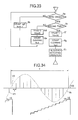
- a digital signal processing system is composed of a sample holder 101, an A/D converter 102, a digital filter 103 and a digital processing unit 104.
- An analog signal is inputted to the sample holder 101 from an analog sensor 100.
- the analog sensor 100 is constructed to convert data of a variety of analog quantities of, e.g., an electric current, a voltage, a speed, a pressure and a temperature into voltages.
- the analog signals of the analog sensor 100 are inputted to the sample holder 101.
- the sample holder 101 sample-holds these signals.
- the held data are then outputted to the A/D converter 102.
- the A/D converter 102 converts the input data into digital data.
- the thus converted data are outputted to the digital filter 103.
- the digital filter 103 effects filtering on the input data, thereby extracting data of a specified frequency component from a group of input data.
- the extracted data is outputted to the digital processing unit 104.
- the digital processing unit 104 Based on the input data, the digital processing unit 104 effects a variety of arithmetic operations.
- the processing unit 104 then outputs the arithmetic results.
- the signal components of the analog signals turned out to contain higher-order harmonic components.
- the analog signals contain noises, so-called disturbance noises induced to a power supply as noise components.
- Such disturbance noises are also caused in an input of the A/D converter 102 as well as in an output of the sample holder 101.
- a waveform at this time is illustrated in FIG. 3B.
- the noise is produced within a passage zone of the analog signal. It could be confirmed that this noise component is generated depending on a frequency that is 1/N (N is the integer larger than 2) as small as the sampling frequency fs.
- a blocking zone T2 of the digital filter 103 is set to have a frequency higher than in a passage zone Ta of the analog signal.
- the sampling frequency fs of the sample holder 101 is so set that a noise generating region associated with a quantization error and the disturbance noises as well is larger than the blocking zone T2 of the digital filter 103. More specifically, where frequencies f1 - f2 are set in the passage zone, a frequency region f2 - 1/2 fs is set to serve as the blocking zone T2.
- the frequency-gain characteristics are set to attenuate, e.g., a portion of the frequencies f2 - 1/2 fs.
- synthesis noises 107 containing the disturbance noises and the noises incidental to the quantization error deviate from the passage zone T1. It was confirmed that the noises 107 are produced within the blocking zone T2 of the digital filter 103. Namely, the synthesis noises can be separated from the analog signal. This in turn makes it possible to process the digital signal with a high accuracy.
- FIG. 4 An embodiment developed from the one shown in FIG. 1 will next be explained referring to FIG. 4.
- a different component is a digital filter 200, and other components are the same as those in the previous embodiment.
- the same components are therefore marked with the like symbols, and the description thereof is omitted.
- the synthesis noises containing both the disturbance noises and the noises concomitant with the quantization error are generated depending on the 1/N frequency (N is the integer) of the sampling frequency fs.
- N is the integer
- zero point frequencies F1 - F6 of the digital filter 200 are set to match with the frequencies of noises 202. Owing to this setting, the noises can be more attenuated.
- all the frequencies, which are contained in the blocking zone T2 and are 1/integer the sampling frequency fs are selected as the zero point frequencies of the digital filter 200.
- only the zero point frequencies assuming higher levels are selectable from actually measured values of the noise levels.
- the synthesis noises are produced at random.
- the zero point frequencies can be set by predicting the frequencies at which a good deal of synthesis noises are caused. Besides, as will be mentioned later, the noise generating frequencies are detected. A configuration and characteristics of the digital filter 200 can be adaptively modified so that the detected frequencies become the zero point frequencies of the digital filter 200.
- the A/D converter 102 is constructed to have a 12-bit resolving power.
- the digital filter 200 exhibiting the characteristics shown in FIGS. 5A and 5B, it is feasible to obtain a resolving power greater than that of the A/D converter 102.
- FIGS. 6 and 7 each show a typical block conceptual configuration of the digital filter 200.
- FIG. 6 illustrates an IIR (Infinite-extent Impulse Response) type filter.
- FIG. 7 illustrates an FIR (Finite-extent Impulse Response) type filter.
- the filter when the degree is secondary, the filter consists of adder blocks 301 through 304, filter coefficient blocks 305 through 309, a delay block 310 for delaying a signal Wn by 1/T (T: period) and a delay block 311 for delaying a signal Wn-1 by 1/T.
- Input signals Xn are subjected to filtering to generate filter output data Yn.
- the filter depicted in FIG. 7 comprises adder blocks 320 and 321, filter coefficient blocks 322 to 324, a delay block for delaying an input signal X'n by 1/T and a delay block 326 for delaying a signal X'n-1 by 1/T.
- the input signals X'n are filtering-processed, and output data Y7n are thereby outputted.
- this embodiment adopts the following arrangement.
- a digital filter means using a DSP digital signal processor
- the arithmetic operation is repeatedly performed per sampling period on the basis of the predetermined filter coefficient.
- the time-division filtering process is effected softwarewise according to the number of input points. It is therefore possible to correspond to an increase or decrease in the number of input points, changes in characteristic and standardization of a printed board. Namely, if a signal system for 12 channels is needed, the analog filters for 12 channels are also required.
- the filter may be constructed softwarewise corresponding to the number of channels.
- Filtering is attainable by employing no analog filter.
- an element such as a resistor or capacitor
- a higher performance can be attained, and any adjustment can be eliminated.
- an externally attached inspection circuit becomes unnecessary. It is feasible to correspond to the changes in characteristic by use of the internal software. In consequence, the manufacturing steps can remarkably be reduced, and the maintenance is also unnecessary.
- the digital filter 200 depicted in FIG. 8 is of an IIR type.
- the Filter 200 can be constructed depending entirely on the coefficients of the filter coefficient blocks 305, 307 and 309.
- the filter is configured as a low-pass filter.
- a coefficient A1 2.0.
- a coefficient A2 1.0
- the filter characteristics e.g., a central frequency f0 and a selectivity Q-are attainable by modifying coefficients B1 and B2 of the filter coefficient block 306 to fulfill desired characteristics.
- FIGS. 9A to 9C show examples of frequency-gain characteristics of a low-pass filter 402, a band-pass filter 403 and a notch filter 403.
- FIG. 10 shows an example where in an initial process indicated by a block 511, a frequency analysis of error is carried out; a filter coefficient to reduce the error is derived; and a normal process indicated by a block 512 is executed based on this filter coefficient.
- a frequency analysis of error is carried out; a filter coefficient to reduce the error is derived; and a normal process indicated by a block 512 is executed based on this filter coefficient.
- the digital data are at first stored in a data memory. At this moment, initialization of clearing of the data memory and the like is effected. There is made a judgment as to whether or not the digital data are inputted from the A/D converter 102 (step 501).
- step 502 When inputting the digital data (step 502), whether n-pieces, e.g., 512 pieces of digital data are inputted or not is judged (step 503). Processes up to the steps 501 - 503 continue till the n-pieces of digital data are inputted.
- a spectrum analysis about the data is carried out (step 504). This spectrum analysis is performed by use of FFT arithmetic (fast Fourier transform).
- the filter coefficients are derived to make the detected frequencies match with the zero point frequencies of the digital filter 200 (step 505).
- the initial process is carried out to make zero the error generating frequency by use of the above-mentioned arithmetic formulae.
- the characteristics and configuration of the filter are determined. Namely, a specific number of stages at which the filter is connected to the cascades is determined.
- the error generating frequency does not largely varies. Hence, even when setting the characteristics and configuration of the filter at the initial time, there is caused no problem in terms of practical use.
- step 506 whether there is a data input interrupt or not is judged (step 506). If the interrupt exists, the data are inputted (step 507). Subsequent to this step, the digital filtering process is executed by using the digital filter coefficients obtained at the initial time, thereby reducing the errors (step 508). The digital operation is performed based on the data in which the input data undergo filtering (step 509) The data pursuant to the arithmetic result are outputted (step 510).
- the frequency analysis of the error is effected at the initial time.
- the filter coefficients are set pursuant to the analytic result. A contrasting arrangement of an embodiment shown in FIG. 11 will be given.
- the error frequency analysis is performed per sampling.
- the filter coefficients are adaptively modified to constantly considerably reduce the error frequency components. The following is an explanation of a concrete example.
- initial setting such as clearing of the data memory is executed (step 600).
- a judgment as to whether there is a data input interrupt or not is made (step 601). If the interrupt exists, the data are inputted (step 602).
- An on-line spectrum analysis is effected based on the input data (step 603). This spectrum analysis helps the error frequency analysis.
- the digital filter coefficients are obtained to reduce the frequency components of the detected noises (step 604).
- the input data undergo the filtering process (step 605).
- the digital operation is carried out based on the filtering-processed data (step 606). This arithmetic result is outputted (step 607). A series of these operations are repeated per period T, thus calculating the digital data.
- the configuration and characteristics of the filter are adaptively modified. It is therefore possible to decrease the noises corresponding to a situation where the noises are produced concomitantly with the quantization error and the disturbance noises caused at random. Besides, the highly accurate digital arithmetic process can be actualized.
- FIG. 12 illustrates a block construction where the digital signal processing system of this invention is applied to an electric power digital protective relay system.
- the system depicted in FIG. 12 incorporates protective relay processing functions allocated to nine kinds of units.
- the digital signal processing system of this invention is applied to an analog input unit 700 among these units.
- These units are a system control unit 605 for a multiprocessor system, the analog input unit 700 for performing an A/D conversion of the analog input and also a digital filtering process, a relay arithmetic unit 701, a sequence processing unit 702, a settle/display processing unit 706, a digital I/0 unit 703, an accident detecting unit 709, an auxiliary relay unit 704 and a surface panel unit 710.
- the units 700 to 702 and 704 to 706 are connected to each other via a general-purpose system bus B1.
- the sequence processing unit is connected to the digital I/0 unit 703 via an I/0 bus B2 different from the system bus B1.
- a relay arithmetic part 707 and a sequence processing part 708 within the accident detecting unit 709 are connected to each other through an I/0 bus B3 different from the buses B1 and B2.
- the system incorporates a power supply unit by which the respective units are driven.
- the electric power system information on, e.g., a voltage and current of a transmission line is inputted. Furthermore, an analog quantity is converted into a digital quantity.
- an electric quantity for detecting or controlling an accident is derived.
- the derivation of the electric quantity includes magnitudes of the voltage and current in the event of the accident in the electric power system, an impedance Z, a resistance R and a reactance X up to the point of time when causing the accident, an accident direction and further an accident frequency.
- the electric quantity derived at the step 2002 is compared with a predetermined settled value to given a comparative judgment. As a result of the comparative judgment, if judged as an accident, the action moves to a step 2004.
- step 2004 whether the accident conditions judged at the step 2003 continue or not is judged. If the conditions continue, the action moves to a step 2005.
- the information is stored because of the judgment as the accident.
- step 2006 system sequence processing (including a combination of a timer with external conditions) is carried out based on a variety of relay operations stored at the step 2005. In the case of the judgment as the accident, a cut-off instruction to a circuit breaker is issued.
- the system is inspected and monitored.
- the electric power digital control protective system repeatedly executes the above-mentioned processes during a period that is n-times (n is the integer) as large as the sampling period T of the analog input.
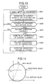
- FIG. 14 shows an example of characteristic a known reactance relay (for one element) and a mho relay (for one element).
- the symbol jx represents an induction reactance of the impedance.
- a the step 2002 approximately 30 to 50 relay elements are processed.
- An expected sequence process corresponding to the system is effected based on the outputs of these relay elements at a step 2006.
- the symbols Z1 and Z2 shown in FIG. 14 designate settled values.
- a protective range is conditional to these values. These settled values are modified on line by handling of a man from outside of the system when modifying the electric power system and the protective range incidental thereto.
- FIG. 15 illustrates an example of a processing flow of the reactance relay depicted in FIG. 14.
- FIG. 16 shows an example of processed waveforms corresponding to the respective processing steps of FIG. 15.
- the symbols S1 through S6 in FIG. 5 correspond to those of FIG. 16.
- step S1 voltage/current data are at first inputted (steps 1 and 2).
- step S3 A variety of arithmetic operations are effected on the voltage-current data (steps S3 - S7).
- the arithmetic results are compared with the settled values (step S8). If the arithmetic results are larger than the settled values, a counter (not illustrated) for examining a duration of an abnormal state is incremented by +1 (step S9).
- step S10 whether a count value of this counter becomes greater than a predetermined count value or not is examined. If greater than the predetermined value, this is judged as a status where the relay should be worked. An output of the element relay is set to 1 (step S11).
- the output of the element relay is set to 0.
- the relay remains non-operated (step S12).
- step S14 If the arithmetic results are smaller than the settled values at the step S8, however, the counter is cleared (step S13). As a matter of course, the output of the element relay is 0 (step S14).
- the symbols 6a-1 through 6a-N represent low-pass filters (employed for preventing a reflected error attributed chiefly to sampling and hereinafter abbreviated to LPFs). These filters serve to input analog signals in1 through inN inputted from outside and also eliminate the higher harmonics overlapped with the input signals.
- the symbols 6b-1 to 6b-N denote sample hold (hereinafter abbreviated to S/H) circuits; 6c a multiplexer (abbreviated to MPX); 6d an analog-to-digital (abbreviated to A/D) converting circuit; and 6e a dual port RAM (DPRAM) based buffer memory for A/D converted data.
- S/H sample hold
- MPX multiplexer
- A/D analog-to-digital
- DPRAM dual port RAM
- the symbol 6f designates a DSP (Digital Signal Processor); 6j a program memory (ROM) for storing an instruction of the DSP 6f; 6h a local bus; 6i a dual port data memory for transferring and receiving the data to and from a system bus; 6k a system bus interface circuit; and 6l a system bus.
- DSP Digital Signal Processor
- ROM program memory
- Designated at 6g is a timing generating circuit for controlling operations of the S/H circuits 6b-1 through 6b-N, the MPX 6c, the A/D circuit 6d and the buffer memory 6e.
- the timing generating circuit 6g also transmits an interrupt signal to the DSP 6f.
- the individual ICs and LSIs can, however, be integrated into one LSI.
- the DPS, ROM, buffer memory and data memory are also integrated into one LSI, thereby remarkably compactly miniaturizing the circuit.
- the digital filter arithmetic operation explained earlier is effected by the DSP 6f of FIG. 17. Namely, the digital filter arithmetic operation, as described before, requires a multiplicity of repetitions of effecting a product-sum operation of decimal point data. For this reason, the DSP capable of performing the product-sum operation at a high speed is preferable.
- the DSP is classified into a fixed point arithmetic type and a floating point arithmetic type.
- the processor for executing the digital filter arithmetic operation is applicable to both types.
- the floating point arithmetic type DSP is more desirable. It is because a wider dynamic range can be secured, and there is no necessity for particular awareness about an overflow or underflow.
- FIG. 18 is a diagram showing in detail a construction of one embodiment of the DSP 6f.
- the DSP in this embodiment comprises: an address register 1200 for specifying an address of an external memory; a data register 1201 used as a parallel port; a data RAM 1203; an (m-bit x m-bit) fast parallel multiplier 1204; a ROM 1205 for instruction; an ALU (Arithmetic Logic Unit) 1207 for performing addition and subtraction; a register 1208 such as an accumulator; a control circuit 1209 for controlling an interrupt of control signals (a, b and c) with respect to the outside; and an internal bus 1210 within the DSP.
- an address register 1200 for specifying an address of an external memory
- a data register 1201 used as a parallel port
- a data RAM 1203 for an (m-bit x m-bit) fast parallel multiplier 1204
- a ROM 1205 for instruction
- an ALU (Arithmetic Logic Unit) 1207 for performing addition and subtraction
- a register 1208 such as an accumulator
- a control circuit 1209 for
- the multiplier 1204 multiplies contents of input signals A and B during one instruction cycle. A result C thereof is outputted to the internal bus 1210.
- the ALU 1207 adds the data from the internal bus 1210 to the data of the register 1208. A result thereof is written to the register 1208.
- the DSP is, as is widely known, capable of carrying out the product-sum operation during one instruction cycle and also effecting pipe line processing.
- the DSP is characteristically able to compute the numeric values of fixed and floating point data at a high speed.
- the general-purpose microprocessor incorporating no floating point arithmetic unit is slow of processing and therefore unapplicable.
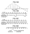
- FIGS. 19A to 19D show examples of a processing timing of the analog input unit depicted in FIG. 17. As illustrated in the Figures, the analog input unit is capable of processing in the following three cases depending on the system applied.
- the digital filter arithmetic operation is performed with a period of 3 kHz. After finishing the digital filter arithmetic operation for 5 samples, the arithmetic results are transferred to the control/protective arithmetic unit. It is feasible to synchronize with the arithmetic unit having a period of 600 Hz.
- the digital filter arithmetic operation is effected with a period of 3 kHz.
- the arithmetic results are transferred to the control/protection arithmetic unit similarly with the period of 3 kHz.
- the control/protective arithmetic operation is carried out with the period of 3 kHz together with the digital filter arithmetic operation. That is, the DSP depicted in FIG. 18 executes the filter and control/protective arithmetic operations. In the second and third cases, the arithmetic processing is thereby speeded up.
- FIG. 20A and 20B show phasic characteristics of a reactance relay applied to a back-up protection of the transmission line.
- FIG. 20A shows the phasic characteristics in the prior art system (the analog filter is applied).
- FIG. 20B shows the phasic characteristics in the system to which this invention is applied. In these two systems, the arithmetic of the reactance relay is based on absolutely the same algorithm.
- the dynamic impedance error (an error of the operated impedance with respect to a settled impedance) at a characteristic angle (phase angle of 90°) exhibits 3 - 4 %.
- This embodiment gives an example where the dynamic impedance error at the characteristic angle exhibits 1 % or less.
- FIG. 21 shows an example of the dynamic impedance characteristics of the reactance relay.
- Solid lines 1501a and 1501b indicate the dynamic impedance characteristics of this invention.
- the imperfect operating zone in the dynamic impedance characteristics of this invention is narrower than in the prior art system. Hence, the accuracy can be extremely increased (high sensitivity). The sensitivity is 3 to 5 times as high as that in the prior art system.
- FIG. 22A and 22B show the physical characteristics when the present invention is applied to an input unit of a distance relay for obtaining a resistor R and a reactance L up to an accident point in conformity with a differential equation.
- FIG. 22A shows an example of characteristics based on the prior art method.
- FIG. 22B shows an example according to the present invention.
- the example to which this invention is applied exhibits such characteristics that a width of the imperfect operating zone between the operating zone and the non-operating zone is quite narrow, and the highly increased accuracy (high sensitivity) is, it can be understood, attainable.
- FIG. 23 shows an example of a process block configuration for detecting voltage effective values of the electric power system, to which this invention is applied.
- the aforementioned DSP 1100 depicted in FIG. 17 arithmetically executes the processes of the respective blocks. This is applied to, e.g., an electric power system voltage/reactive power control system.
- the numeral 1701 denotes a digital filter processing block to which this invention is applied. Attenuated in this block are the higher harmonics overlapped with the input signals Vi, offset components, the disturbance noises and the quantization error.
- the filter coefficients are set so that low-order harmonics which are n-times (multiple of integer) the fundamental harmonics, the disturbance noises and the quantization error frequency becomes zero point frequencies of the digital filters or come to the vicinity thereof. A large amount of attenuation is thus obtained.
- a signal frequency is obtained in a block 1702 by using the filtering-processed data.
- an input data frequency i.e., an electric power system frequency fluctuates ( + 1 through 3 Hz). It is therefore necessary to correct a gain which fluctuates due to the frequency characteristics of the digital filter.
- the gain of the input data is corrected by employing the frequency obtained in the block 1702.
- Obtainment of the peak value involves the use of, for instance, a peak value holding method or the following arithmetic equation.
- the effective value is acquired by use if the peak value in a block 1705.
- An averaging process is effected for increasing the accuracy in a block 1706.
- the effective value of the input data can be obtained with an accuracy of 0.01 % or under.
- the digital filter, shown in the block 1701, to which this invention is applied is indispensable for attaining the increased accuracy.
- the data is inputted at a step 1801.
- Effected thereafter at a step 1802 is the arithmetic process of the digital filter to which this invention is applied.
- the frequencies at which the disturbance noises and the quantization error are generated fall within the blocking zone of the digital filter.
- the voltage effective value detection shown in a step 1803 is subjected to no adverse influence.
- the voltage effective value is obtained by performing the following arithmetic:
- the sampling frequency is varied corresponding to the frequency of the input signal.
- the algorithm is therefore constant irrespective of the frequency of the input signal.
- the detected voltage effective value is outputted at a step 1804.
- FIG. 25 shows an example of frequency-gain characteristics of the digital filter used at the step 1802.
- a characteristic 1805 is modified into a characteristic 1806, corresponding to a change in the frequency of the input signal from the electric power system.
- the frequencies at which the disturbance noises and the quantization error are caused change in proportion to the sampling frequencies. Hence, the error reductive effects remain as they are.
- the voltage effective value can, as a matter of course, be detected with an extremely high accuracy.
- FIG. 26 there is illustrated a signal analyzing system.
- physical quantities (displacement, velocity, pressure, temperature, etc) are transduced into electric potentials by means of a transducer 3001.
- Outputs of this transducer 3001 are typically digitized at regular time intervals. That is, the outputs thereof are converted into digital quantities by an A/D converter 3002.
- a digital filter 3004 eliminates the high frequency components of the A/D converted data or extracts the specific signal frequency components, thereby obtaining the highly accurate data.
- the numeral 3005 represents a correlating unit for seeking correlation functions between the signal taken in and other signals.
- the present invention is applicable to the portion for filtering after effecting the A/D conversion.
- the highly accurate signal analyzing system e.g., the spectrum analyzer
- the spectrum analyzer can be therefore constructed.
- FIG. 27 illustrates an example of configuration of a voice signal processing system, i.e., a CODEC (coderdecoder) system.
- CODEC coderdecoder
- a voice signal is taken in by an analog sensor 4001.
- the voice signal is, after being A/D converted by an A/D converter 4002, subjected to a process such as echo canceling in a digital signal processor 4003.
- the voice signal is D/A converted into an analog signal by a D/A converter 4004.
- Analog control is performed by an analog controller 4005 with the aid of the analog signal.
- this invention is applicable to the portion for echo canceling by use of the digital signal processor as well as to the A/D converting portion.
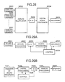
- FIG. 28 shows an example of configuration of a digital data recorder system.
- a plurality of analog input signals are taken in by an analog sensor 5001. These signals are changed over by an analog multiplexer 5002 and sequentially A/D converted by an A/C converter 5003. The thus converted signals undergo digital signal processing by a digital signal processor 5004. The resultant data are stored in a recorder 5005.
- the present invention is applicable to the portions relative to the A/D conversion and the digital signal processor.
- the input signals are storable with a fidelity.
- FIGS. 29A and 29B show examples of a digital audio system.
- a sound source 6001 is processed by an analog processing unit 6002.
- the resultant signals are A/D converted by an A/D converter 6003.
- the data thereof are subjected to digital processing in a processing unit 6004 preparatory to recording by a sound recorder 6005.
- a processing unit 6004 When reproducing the sound, more digitally recorded signals 7001 are processed in a processing unit 7002.
- the data thereof are D/A converted by a D/A converter 7003.
- the analog signals are then processed in a processing unit 7004 and thereby outputted as a sound from a speaker 7005.
- the present invention is applicable to portions associated with digital processing and the A/D conversion in the sound recording system. It is therefore feasible to record the sound source with a fidelity. A signal-to-noise ratio (S/N ratio) is remarkably improved.
- an adaptive digital filter 1a is configured as a gain variable type filter. Inputted to this filter 1a an output signal from an analog-to-digital converter for converting an output signal of a sample holder for sample-holding an AC signal into a digital signal.
- the digital filter 1a effects filtering on the digital signal inputted.
- the filter 1a extracts signals of specific frequency components from the digital signal components.
- the extracted signals are outputted to a peak value detection processing unit 1b and a frequency detecting processing unit 1d.
- a peak value of the AC signal is detected from the output signals of the filter 1a. On this occasion, the peak value is also obtained by detecting the maximum value per half-cycle of the output signals of the filter 1a.
- a peak value V is obtained in conformity with the following formula (17) to eliminate an influence by sampling phase: where Va and Vb are the sample values of arbitrary continuous two points, ⁇ is the input angle frequency and ⁇ t is the sampling interval.
- the output signal of the peak value detecting processing unit 1b is inputted to an effective value arithmetic unit 1c.
- an effective value Vrms is calculated based on the peak value V in accordance with the following formula (18):
- the output signal of the filter 1a is inputted to the frequency detection processing unit 1d, wherein a frequency of the AC signal is detected. Based on this detected result, a filter coefficient calculation processing unit 1e calculates such a filter coefficient that the detected frequency coincides with a central frequency (gain is go) of the digital filter 1a. In accordance with the calculated filter coefficient, the gain characteristics of the digital filter 1a are adjusted.
- the frequency of the input signal taken in from the electric power system is indicated by a characteristic 2a.
- the filter coefficient is calculated so that the fundamental frequency of the AC signal coincides with a zero point frequency fo of the digital filter 1a.
- the filter coefficient is calculated according to the detected frequency fo'.
- the gain characteristics of the digital filter 1a are adjusted based on this filter coefficient. Namely, the filter characteristic becomes one indicated by a characteristic 2b. Even when the AC signal frequency fluctuates, it is possible to sufficiently attenuate higher-harmonic components (the second, third, fourth ... ) of the AC signals.
- a gain (output-to-input ratio) of the AD signal inputted to the digital filter 1a can be kept constant.
- the effective value is obtained from the output signal of the digital filter 1a, and hence it follows that the effective value can be acquired with the high accuracy without depending on the fluctuations in the frequency.
- FIGS. 32A and 32B show typical block conceptual configurations of the digital filter.
- FIG. 32A depicts an IIR (Infinite-extent Impulse Response) type filter.
- FIG. 32B illustrates an FIR (Finite-extent Impulse Response) type filter.
- the symbol Xn represents an input signal; 3a each coefficient block; K a gain coefficient; and A1, A2, B1 and B2 filter coefficients.
- the symbol 3b denotes a delay block.
- the delay block is classified into a block (Wn-1) for delaying the signal Wn by one timing of a period T and a block (Wn-2) for delaying the same signal by 2 timings of the period T.
- the symbol 3C designates an adder block.
- the symbol Yn represents filter output data.
- the symbol X'n represents input data, while Y'n designates output data.
- Designates at 3d is a delay block classified into a block X n-1 for delaying the signal by one timing of the period T and a block X n-2 for delaying the signal by 2 timings of the period T.
- the symbols 3e indicate filter coefficient blocks. Respective filter coefficients are set at A' 0 , A' 1 and A' 2 .
- the symbol 3f represents an adder block.
- this embodiment takes the following arrangement.
- the digital filter means using the DSP digital signal processor
- the arithmetic operation is repeatedly performed per sampling period on the basis of the preset filter coefficient.
- the time-division filtering process is effected softwarewise according to the number of input points. It is therefore possible to correspond to an increase or decrease in the number of input points, changes in characteristic and standardization of a printed board.
- Filtering is attainable by employing no analog filter. Hence, there exists absolutely no factor for an initial value deviation, as seen in the analog filter, of an element such as a resistor or capacitor, fluctuations in the element value due to the ambient temperatures and a deterioration of the element because of reductive changes. A higher performance can be attained, and any adjustment can be eliminated.
- an externally attached inspection circuit becomes unnecessary. It is feasible to correspond thereto with the internal software. This remarkably reduces the number of manufacturing steps. The maintenance is also unnecessary. Considerable merits are created, wherein the protective relay system increases in accuracy, and the costs are decreased.
- Table 1 shows arithmetic equations for obtaining the respective coefficients of the low-pass notch filter, the low-pass filter and the band-pass filter.
- step 5b the output signals of the digital filter 1a are sequentially taken in. Whether the input data are zero-crossed or not is judged (step 5b). This count value indicates the number of sampling operations during one period of the input data.
- step 5c when the input data are zero-crossed, whether or not the zero-cross is the second time is judged (step 5c). More specifically, a process of detecting the zero-cross for one period is executed. If the zero-cross is not the second time-viz., the zero-cross is the first time, data V(t-1) before one timing is set as V1. Data V(t) at the present time is set as V2 (step 5d). Thereafter, the counter value is cleared (step 5e). To be specific, the count values counted up per sampling are set to zero. The count-up resumes from a point of time when effecting the zero-cross.
- step 5f the count values of the counter are set to zero (step 5g).
- the arithmetic detection of the frequency is executed based on the counter value (step 5h).
- the frequency f is given in the following formula (27) by using the positive and negative voltages V1, V2, ,V3 and V4 at the zero-cross, the input signal sampling number k within one period and the sampling period T:
- ⁇
- ⁇
- the sampling frequency is increased by a factor of greater than 24 over the fundamental frequency (50 or 60 Hz) of the AC signal, whereby the detection accuracy can be enhanced.
- the embodiment discussed above has made use of a point at which the zero-crossed input data changes from the negative to the positive. Another available arrangement is that a point at which the input data changes from the positive to the negative is set as a zero-cross. The zero-cross can be also detected in a state where these two arrangement are combined.
- FIGS. 17 and 18 The usable hardware for embodying the present invention is shown in FIGS. 17 and 18.
- the systems depicted in FIGS. 17 and 18 detect the electric quantities of the AC signals, e.g., an effective value of the AC voltage.
- the AC signals are inputted to a low-pass filter 6a.
- Output signals of the low-pass filter 6a are taken in a sample hold circuit 6b.
- These signals are sequentially sampled by use of sampling signals of the sampling period T which are outputted from a timing signal generating circuit 6g.
- the sample-held signals are inputted via a multiplexer 6c to an analog digital converting circuit 6d.
- the analog signals are converted into digital data.
- the thus converted data are stored in a buffer memory 6e.
- the digital data stored in the buffer memory 6e are sequentially transferred to a processor 6f.
- the processor 6f performs a peak value detecting operation, an effective value calculating operation, a filter detecting operation and a filter coefficient calculating operation. More specifically, the peak value of the AC signal is detected based on the input data. Simultaneously, the effective value is detected based on the peak value. If the input data are zero-crossed, the frequencies of the AC signals are detected. A variety of filter coefficients are calculated based on the detected frequencies. The frequency is obtained at every one cycle-passage of the output signal. Hence, the filter coefficient can be obtained during one cycle. After obtaining all the filter coefficients, the new filter coefficients are employed instead of the old ones. The frequency-gain characteristics of the digital filter 1a are then adjusted.
- the gain of the filter is adjusted at the constant level corresponding to the fluctuations in the frequency of the input signal in the present invention. Even when the frequency of the input signal fluctuates, the effective value detection error can be reduced. Whereas in the case of employing the gain-fixed type digital filter, the detection error decreases when the input signal frequency is 50 Hz but increased as the frequency moves away from 50 Hz.
- the respective filter coefficients can also be obtained per sampling. If an extra processing time is prepared, all the coefficients are obtainable at one time.
- the processor 6f incorporates a filter coefficient bank 10a for storing the data of a group of coefficients corresponding to the detection frequencies of, e.g., 45 through 55 Hz.
- a specified filter coefficient corresponding to the detection frequency is selected from the coefficient bank 10a.
- the selected filter coefficient is transferable to the digital filter 1a. In this instance, the arithmetic operation for obtaining the coefficients is unnecessary, thereby quickly modifying the gain characteristics of the digital filter 1a.
- the processor 6f includes a gain-fixed type digital filter 11a.
- the frequency of the input signal is detected from an output signal of the digital filter 11a.
- a filter coefficient is calculated in accordance with this detected frequency. Based on the calculated filter coefficient, the frequency-gain characteristics of the adaptive digital filter 1a are also adjustable. In this case, the frequency of the input signal is detected from the output signal fo the digital filter 11a. For this reason, the digital filter 1a can be more stabilized.
- a gain correction processing unit 12a is interposed between the digital filter 1a and the peak value detection processing unit 1b.
- the gain correction processing unit 12a corrects, to a constant value, a signal gain for the fundamental frequency among the output signals of the digital filter 1a. Owing to this correction, the peak value and the effective value can be detected with a high accuracy even if the gain of the digital filter 1a can not be kept constant in relation to the sampling frequency and the cut-off frequency of the filter 1a.
- a voltage/power control system VQC takes in the AC signals of the electric power system via a current transformer CT and a potential transformer PT.
- the AC signals are sampled and converted into digital signals.
- the effective values of the AC signals are calculated from the thus converted digital data.
- a voltage and reactive power of the electric power system are obtained from this effective values.
- a variety of units are controlled based on the calculated voltage and reactive power.
- the control system VQC as illustrated in FIG.
- a Q-detecting unit 14a comprises: a Q-detecting unit 14a; a V-detecting unit 14b; adders 14c and 14d; a program setting unit 14e; an integration relays 14j, 14g and 14h; an operating unit judgment/logic circuit 14i; an LR control circuit 14j; a capacitor SC for electric power; a shunt reactor ShR; and a control circuit 14k.
- a Q-detecting unit 14a Used therein are the Q-detecting unit 14a and the V-detecting unit 14b incorporating the same functions as those of the processor 6f. With this arrangement, the reactive power and the effective value of the voltage are detectable with the high accuracy.
- a target voltage value and reactive power value are set beforehand in the control system VQC.
- the control system VQC controls a reactive power controller and an LR tap so that the input signal is applicable to the target value. More specifically, a deviation of a detected value from the target value is corrected while following up a voltage/reactive power flow pattern on the basis of a certain prediction.
- a load voltage regulation transformer LRT, the electric power capacitor SC and the shunt reactor ShR are adjustably controlled. Note that the priority is generally given to keeping of the target voltage. Simultaneously, a loss in power transmission is reduced.
- a digital signal processing system 15 in this embodiment is constructed of analog sensors 16a through 16n, A/D converters 17a through 17n and a digital signal processor 18a. An output of the processor 18a is connected via D/A converters 19a through 19n to analog control circuits 20a through 20n.
- the system in this embodiment transforms physical quantities such as oscillations and the like into electric signals with the help of the analog sensors 16a to 16n.
- the transformed electric signals are converted into digital signals by the A/D converters 17a - 17n.
- a variety of arithmetic operations are executed in the processor 18a. Namely, there are obtained the effective values of the AC signals which have been detected by the respective analog sensors. Generated are signals for controlling a variety of loads in accordance with these effective values.
- the generated digital signals are outputted via the D/A converters 19a - 19n to the analog control circuits 20a - 20n, thus controlling the various loads.
- the effective values of the AC signals detected by the analog sensors can be obtained with the high accuracy. This in turn makes it possible to control the loads with the high accuracy.
- a digital multimeter 21 comprises an analog sensor 22, an A/D converter 23, a digital signal processor 24 and a display unit 25.
- a voltage and current of the AC signals detected by the analog sensor 22 are converted into digital signals by the A/D converter 23.
- the digital signals are inputted to the processor 24, wherein the effective values of the voltage and current of the AC signals are calculated.
- the calculated effective values of the voltage and current are displayed on a screen of the display unit 25.
- the effective values of the AC signals detected by the analog sensor 22 can be obtained with the high accuracy. This contributes to an improvement of the measuring accuracy.
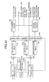
- FIG. 45 is a block diagram depicting a whole construction of an analog input unit to which the digital signal processing system of this invention is applied.
- This analog input unit works to take in the input signals of a voltage and current of the electric power system. Desired physical quantities are obtained by effecting predetermined input processing and outputted to other units such as a control unit, a protective relay unit and the like.
- the analog input unit in this embodiment consists of: a reflected error protective filter 6a for a plurality of channels; a sample hold circuit (S/H) 6b for a plurality of channels in a full-channel simultaneous sampling method; a multiplexer (MPX) 6c; an analog-to-digital (A/D) circuit 6d; a dual port buffer memory 6e using a dual port random access memory (hereinafter abbreviated to DPRRAM); a timing generating circuit 6g; and an interface circuit 6m for synchronizing the units with each other and also the analog unit with other systems (input signals, etc).
- the analog input unit further includes: a digital signal processor (hereinafter abbreviated to DSP) 6f; a program memory 6j for use with the DSP 6f; a DPRAM-based dual port data memory 6i; a system bus interface circuit 6k; an interrupt generating circuit 6n; and an abnormality detecting circuit 6p.
- DSP digital signal processor
- a signal line ⁇ serves to transmits an interrupt generating signal for taking in the data to a system bus 61.
- An abnormality informing/discerning signal (SYS FAIL) is transmitted via a signal line e to the system bus 6l.
- the buffer memory 6e Connected to a local bus 6h are the buffer memory 6e, the DSP 6f, the program memory 6j, the dual port data memory 6i, the interrupt generating circuit 6n and the abnormality circuit 6p.
- the interrupt generating circuit 6n and the abnormality detecting circuit 6p are also connected to the system bus 6l.
- the dual port data memory 6i is connected via the system bus interface circuit 6k to the system bus 6l.
- the DSP 6f in this embodiment is constructed as shown in FIG. 18.
- the DSP 6f is capable of effecting a product-sum operation during one instruction cycle and further pipe line processing.
- the DSP 6f is characterized by its capability of actualizing a fast numeric value operation of fixed and floating point data. It is therefore feasible to perform filtering in real time on the input data at a multiplicity of input points. In this respect, the DSP 6f exhibits a processing velocity higher than that of the general-purpose microprocessor and is therefore preferable.
- FIG. 46 illustrates a detailed block configuration of a digital signal processing system defined as the principal in this embodiment. Processes in the illustrated individual blocks are attained by the DSP 6f. In this embodiment, there is given a means for detecting the voltage effective value of the electric power system on the basis of the input voltage signal.
- a digital filter 30A takes in electric power system voltage signals Vi sampled with a constant period and undergoing a digital conversion from the buffer memory 6e. Offset components and high frequency components overlapped with the input signals Vi are subjected to filtering and thereby eliminated. It is to be noted that in this embodiment the sampling period T of the input signal is set smaller than 1/24 (electric angle of 15°) of one cycle of the fundamental harmonic of the Ac signal in order to enhance the detection accuracy. Filter characteristics are so set that particularly the lower-harmonic which is n-times (n is the integer) as large as the fundamental harmonic coincides with the zero point frequency of the digital filter 30A.
- a subsequent frequency detecting means 30B arithmetically seeks a frequency of the input voltage signals Vi undergoing the filtering process.
- a gain correcting means 30C provided at the next stage is possessed of gain correction data set based on the frequency-gain characteristics.
- the gain correcting means 30C corrects the gain of the filtering-processed voltage signal Vi by use of a correction coefficient corresponding to the foregoing procured frequency.
- a peak value detecting means 30D subsequent thereto detects a peak value of the gain-corrected voltage signal Vi at, e.g., every half-cycle.
- An effective value arithmetic means 30E arithmetically obtains the effective value from the detected peak value.
- An averaging processing means 30F subsequent thereto averages the effective values procured per, e.g., half-cycle to further enhance the detection accuracy.
- the thus obtained effective values of the voltage signals Vi are stored in the data memory 6i. These stored values are used as data for the protective relay as well as for controlling the electric power system.
- Usable filters as the digital filter 30A are depicted in FIGS. 32A and 32B.
- the input signals undergo filtering by the digital filter 30A in combination with the DSP 6f.
- Filtering is repeatedly carried out per sampling period T on the basis of the preset filter coefficients.
- the time-dividing filtering process can be performed softwarewise corresponding to the number of input points. It is possible to correspond to the increase or decrease in the number of input points, the modifications in the characteristics and the standardization of the printed board.
- Filtering is attainable by employing no analog filter. Hence, there exists absolutely no factor for an initial value deviation, as seen in the analog filter, of an element such as a resistor or capacitor, fluctuations in the element value due to the ambient temperatures and a deterioration of the element due to a change with a passage of time. A higher performance can be attained, and any adjustment can be eliminated.
- FIG. 47 shows an example of the frequency-gain characteristics of the digital filter 30A.
- a system frequency of the electric power system is adjusted to a central frequency fo of the filter.
- the symbol go represents a gain at that time.
- a frequency that is n-times (n is the integer) as high as the system frequency is set to the zero point frequency of the digital filter.
- the gain characteristic exhibits a convex curve in the vicinity of the central frequency fo.
- the frequency detecting means 30B has the same construction as that of the frequency detection processing unit 1d depicted in FIG. 30.
- the frequency detecting means 30B is capable of detecting the frequency by executing the processes shown in FIGS. 33 and 34.
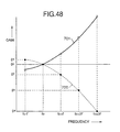
- the gain correcting means 30 of FIG. 46 will be explained with reference to FIG. 48.
- the axis of abscissa indicates the system frequency, while the axis of ordinate indicates the gain.
- a curve 700 indicated by a dotted line in the figure shows a frequency-gain characteristic in the vicinity of the central frequency fo of the digital filter 30A.
- a gain of the central frequency fo is shown by go.
- the symbol g1 indicates a gain of a frequency (fo-f'); g2 represents a gain of a frequency (fo + f'); g3 denotes a gain of a frequency (fo + 2f'); and g4 represents a gain of a frequency (fo + 3f').
- a broken line 701 in the Figure is conceived as an approximate line for correcting the gain characteristics. Namely, this approximate line shows a correction function y for an adjustment to a constant gain by correcting the gain of the detected frequency to the gain go of the central frequency fo.
- the correction function y is expressed by the following formula: where Kg and Kb are the correction coefficients.
- correction coefficients Kg and Kb are set in the following manner by previously examining the characteristics of the digital filter 300:
- an arithmetic period of the frequency correcting operation is identical with or larger than that of the peak detecting operation.
- Designated at 800 is an input signal of the peak value detecting means 30D, i.e., a gain-corrected input signal V.
- Vm1 - Vm3 absolute peak values
- va and vb be the input signals inputted with a sampling period ⁇ t interposed therebetween.
- vb Vp sin ⁇ (t + ⁇ t) (33) where ⁇ is the angular frequency of the input signal.
- vb va cos ⁇ ⁇ t + Vp cos ⁇ t.sin ⁇ ⁇ t (34)
- a sum thereof is obtained by squaring the formulae (32) and (35), respectively.
- the result is given by:
- the peak value Vp can arithmetically procured by the following formula:
- the arithmetic period for the peak value Vp may be identical with the sampling period T of the input signal but may also be longer than the period T-viz., the arithmetic may be effected by thinning out the data.
- the averaging processing means 30F depicted in FIG. 46 takes an average, for a constant period, of the effective values Vrms acquired by the effective value arithmetic means 30E. An average effective value is then outputted.
- the frequency of the filtering-processed voltage signal is detected based on the frequency-gain characteristics of the digital filter 30A.
- the gain of the output voltage signal of the digital filter 30A is thereby corrected.
- An effect is therefore produced, wherein the peak value or the effective value is detectable from the voltage signal with a high accuracy even when the system frequency fluctuates.
- the sampling period T of the input signal Vi is twice or above as high as the conventional 600 Hz (or 720 Hz). Furthermore, the detection accuracy of the peak value or the effective value can be enhanced.
- the correction corresponding to the frequency-gain characteristics of the filter is carried out.
- the sampling period is reduced by use of the digital signal processor.
- the effective value of the system voltage is detectable with a high accuracy without performing the interpolating operation of the complicated algorithm.
- the highly accurate input signal processing system can be actualized with no increase in size.
- the detection accuracy can be improved from 1 - 5 % (12-sampling/one cycle) in the prior art to 0.1 % (60-sampling/one cycle).
- the problems incidental to the analog filter of the RC active filter consisting of a resistor and a capacitor are obviated.
- the problems include, for instance, a scatter in the element, deteriorations both in temperature characteristics and in property due to a change with a passage of time, or an inter-channel scatter in property.
- the accuracy of the input filter can be increased: and the quantization errors can remarkably be reduced.
- the digital filter is not essentially characteristic of the present invention. Hence, the advantages relative to the gain correction according to this invention can be exhibited even when replacing the digital filter 30A of FIG. 46 with an analog filter.
- a function to correct the gain which corresponds to the gain correcting means 30C in the embodiment of FIG. 46 may be incorporated everywhere in rear of the frequency detecting means 30B of the embodiment shown in FIG. 46.
- this function may be inserted on the output side of the peak value detecting means 30D or the effective value arithmetic means 30E.
- FIG. 46 has dealt with the arrangement that the function is accomplished by using the DSP 6f. Instead, the function can be apparently attained by a general-purpose processor or a combination of this general-purpose processor and a coprocessor (floating point operation processor).
- digital filter 30A preferably involves the use of a fast DSP in terms of effecting the filtering process while reducing the sampling period. Therefore, the digital filter 30A and the frequency detecting means 30B are actualized by the DSP 6f of FIG. 45.
- the processes subsequent to the gain correcting means 30C are performed by the general-purpose processors provided in other units.
- FIG. 50 is a block diagram showing another embodiment of this invention.
- FIG. 50 illustrates only the components corresponding to those of FIG. 46. These components are means actualized by the DSP 6f of FIG. 45.
- a different arrangement in this embodiment from FIG. 46 is that the effective value is directly detected without detecting the peak value.
- the same functions and the blocks having the same configurations as those of FIG. 46 are marked with the like symbols, and the description is therefore omitted.
- An effective value arithmetic means 30G depicted in FIG. 50 computes the effective value Vrms by the following formula (39).
- the symbol Vfil represents an output voltage signal, indicated by a waveform 800 of FIG. 51, of the digital filter 30A.
- the symbol n denotes the number of sampling operations, and N represents the number of sampling data for the arithmetic operation.
- a variation in the effective value Vrms procured above is indicated by a waveform 1000 in FIG. 51.
- the thus obtained effective value Vrms exhibits such a characteristic that the gain thereof, as indicated by a line 1100 of FIG. 52, changes corresponding to variations in the system frequency.
- the gain-change depending on the frequency are corrected by a gain correcting means 30A disposed next in accordance with a correction function shown by a line 1101 of FIG. 52.
- the correction herein is carried out in the same procedures as those in the embodiment of FIG. 46. In this embodiment, however, a different point lies in the correction of the effective value Vrms.
- the gain correction is originally needed also in effective value operation processing of FIG. 46, it is possible to correct the gain in accordance with the frequency gain correction of the digital filter after calculating the effective value in this embodiment. The accuracy is thereby improved.
- the effective value is directly acquired without detecting the peak value, resulting in the advantage that the detection accuracy rises.
- FIG. 53 is a block diagram showing still another embodiment of the present invention.
- FIG. 53 shows only the components corresponding to those of FIG. 46. These components are conceived as means actualized by the DSP 6f.
- the peak value detecting means 30D through the averaging processing means 30F are the same as those shown in FIG. 46, and hence the description thereof is omitted.
- a different point of this embodiment from FIG. 46 is that the frequency-gain characteristics of a digital filter 30A1 are different from those of FIG. 46.
- a filter operation program and filter coefficients are adjustably set.
- this embodiment eliminates the necessity for the frequency detecting means 30B and the gain correcting means 30C or 30H which are used in the embodiments of FIG. 46 and 50.
- the characteristics shown in FIG. 54 are procured by improving the characteristics of the digital filter illustrated in FIGS. 32A and 32B. The filtering operation becomes more intricate than in the FIGS. 32A and 32B. The error concomitant with the gain correction does not, however, intervene, whereby the accuracy can be further increased.
- FIG. 55 is a block diagram showing a further embodiment of the present invention. This embodiment takes such a form that the embodiment of FIG. 49 is combined with the digital filter 30A1 used in the embodiment of FIG. 52. The same high accuracy as that in the embodiment of FIG. 53 is acquired.
- the input filter involves the use of the digital filter 30A or 30A1.
- the analog filter is applicable.
- the outputs of the analog filter are sampled at a high speed (e.g., 24 times/one cycle) and then converted into the digital signals. Thereafter, the digital signals undergo the processes shown in the respective embodiments, thereby obtaining the voltage effective values from the voltage signals.
- the frequency-gain characteristics of the filter are compensated, with the result that the voltage effective value can be detected with the high accuracy.
- FIG. 56 shows an example of control characteristics of the VQ control system. Under the control thereof, a target voltage and a reactive power value are at first set. A reactive power controller is set to match with these set values. Then, the reactive power controller and an LR tap are controlled to match therewith. Typically, the priority is given to maintenance of the target voltage. Simultaneously, there is made an attempt to reduce a loss in power transmission. The operating principle will be explained. While following up a voltage/reactive power flow pattern determined based on a certain prediction, a deviation of the target value from a real value is corrected under the adjustable control of a transformer tap, an electric power capacitor and a shunt reactor.
- the voltage effective value is detectable with the high accuracy. This in turn makes it possible to control the voltage/reactive power with the high accuracy.
Landscapes
- Engineering & Computer Science (AREA)
- Power Engineering (AREA)
- Physics & Mathematics (AREA)
- General Physics & Mathematics (AREA)
- Computer Networks & Wireless Communication (AREA)
- Signal Processing (AREA)
- Emergency Protection Circuit Devices (AREA)
- Measurement Of Current Or Voltage (AREA)
- Noise Elimination (AREA)
- Analogue/Digital Conversion (AREA)
Applications Claiming Priority (6)
| Application Number | Priority Date | Filing Date | Title |
|---|---|---|---|
| JP6685/90 | 1990-01-16 | ||
| JP00668590A JP3180190B2 (ja) | 1990-01-16 | 1990-01-16 | ディジタル信号処理方法及びその装置 |
| JP35785/90 | 1990-02-16 | ||
| JP03578590A JP3256805B2 (ja) | 1990-02-16 | 1990-02-16 | 電力系統の信号処理装置、電力制御装置 |
| JP6493990A JP2987635B2 (ja) | 1990-03-15 | 1990-03-15 | ディジタル信号処理方法及びその装置 |
| JP64939/90 | 1990-03-15 |
Publications (3)
| Publication Number | Publication Date |
|---|---|
| EP0437861A2 true EP0437861A2 (de) | 1991-07-24 |
| EP0437861A3 EP0437861A3 (en) | 1993-12-29 |
| EP0437861B1 EP0437861B1 (de) | 1996-06-05 |
Family
ID=27277289
Family Applications (1)
| Application Number | Title | Priority Date | Filing Date |
|---|---|---|---|
| EP90125863A Expired - Lifetime EP0437861B1 (de) | 1990-01-16 | 1990-12-31 | Verfahren und System zur digitalen Signalverarbeitung. |
Country Status (5)
| Country | Link |
|---|---|
| US (1) | US5255202A (de) |
| EP (1) | EP0437861B1 (de) |
| KR (2) | KR100224185B1 (de) |
| CA (1) | CA2033874C (de) |
| DE (1) | DE69027292T2 (de) |
Cited By (8)
| Publication number | Priority date | Publication date | Assignee | Title |
|---|---|---|---|---|
| FR2691314A1 (fr) * | 1992-05-14 | 1993-11-19 | Soule Sa | Carte de télécommande, notamment pour interrupteur aérien. |
| WO1997009626A1 (de) * | 1995-09-04 | 1997-03-13 | Siemens Aktiengesellschaft | Elektrizitätszähler |
| EP0871036A3 (de) * | 1997-04-09 | 1999-03-31 | Fluke Corporation | Eingangsarchitektur für ein Messgerät |
| EP1039304A3 (de) * | 1999-03-19 | 2004-02-04 | MASCHINENFABRIK REINHAUSEN GmbH | Messverfahren für eine Hochspannungsdurchführung und geeignete Messanordnung |
| CN104934923A (zh) * | 2015-06-30 | 2015-09-23 | 安徽博诺思信息科技有限公司 | 一种微电网继电保护装置 |
| CN105116220A (zh) * | 2015-07-30 | 2015-12-02 | 中国电子科技集团公司第四十一研究所 | 同步分离信号与噪声的信号分析装置及其分析方法 |
| EP2955835A1 (de) * | 2014-06-12 | 2015-12-16 | Actron Technology Corporation | Kurzschlussdetektionsschaltung und Kurzschlussdetektionsverfahren für mehrphasige Gleichrichter im Frequenzbereich |
| CN105223459A (zh) * | 2014-06-06 | 2016-01-06 | 朋程科技股份有限公司 | 在频域中多相整流器的短路检测电路及短路检测方法 |
Families Citing this family (35)
| Publication number | Priority date | Publication date | Assignee | Title |
|---|---|---|---|---|
| JP3177978B2 (ja) * | 1990-07-18 | 2001-06-18 | カシオ計算機株式会社 | デジタルフィルタの係数設定方法 |
| JP2773601B2 (ja) * | 1993-06-11 | 1998-07-09 | ヤマハ株式会社 | 信号処理装置 |
| US5907241A (en) * | 1996-09-11 | 1999-05-25 | Abb Power T&D Company Inc. | Current measurement methods and apparatus employing second harmonic scaling |
| US6263288B1 (en) | 1998-07-22 | 2001-07-17 | Eastman Kodak Company | Method and apparatus for indicating proximity of film scanner to CRT display monitor |
| JP2000241202A (ja) * | 1999-02-24 | 2000-09-08 | Denso Corp | センサ装置 |
| JP3862918B2 (ja) * | 1999-06-22 | 2006-12-27 | シャープ株式会社 | フィルタ回路 |
| JP2001045646A (ja) * | 1999-07-28 | 2001-02-16 | Toshiba Corp | ディジタル保護継電器 |
| US6460001B1 (en) * | 2000-03-29 | 2002-10-01 | Advantest Corporation | Apparatus for and method of measuring a peak jitter |
| US7701683B2 (en) | 2001-07-06 | 2010-04-20 | Schweitzer Engineering Laboratories, Inc. | Apparatus, system, and method for sharing output contacts across multiple relays |
| US6480126B1 (en) * | 2001-10-26 | 2002-11-12 | Agilent Technologies, Inc. | Phase digitizer |
| US7346126B2 (en) * | 2001-11-28 | 2008-03-18 | Telefonaktiebolaget L M Ericsson (Publ) | Method and apparatus for channel estimation using plural channels |
| CA2453292A1 (en) * | 2004-01-07 | 2005-07-07 | John W. Bogdan | Noise filtering edge detectors |
| JP4011041B2 (ja) * | 2004-06-16 | 2007-11-21 | Necエレクトロニクス株式会社 | アナログ・デジタル変換システムと補正回路及び補正方法 |
| DE102004036069B4 (de) * | 2004-07-24 | 2017-04-06 | Dr. Johannes Heidenhain Gmbh | Verfahren und Vorrichtung zum Bilden von rauschgefilterten Ausgangswerten aus rauschbehafteten Eingangswerten |
| KR100666491B1 (ko) * | 2005-05-11 | 2007-01-09 | 엘에스산전 주식회사 | 디지털 필터링을 이용한 주파수 검출 방법 |
| US20070164753A1 (en) * | 2006-01-18 | 2007-07-19 | International Business Machines Corporation | Power supply history monitor |
| US7567881B2 (en) * | 2007-03-30 | 2009-07-28 | General Electric Company | Self-adjusting voltage filtering technique compensating for dynamic errors of capacitive voltage transformers |
| US8504130B2 (en) * | 2008-10-07 | 2013-08-06 | Covidien Lp | Non-interfering physiological sensor system |
| US9256232B2 (en) | 2009-06-12 | 2016-02-09 | Schweitzer Engineering Laboratories, Inc. | Voltage regulation using multiple voltage regulator controllers |
| US8427131B2 (en) | 2009-06-12 | 2013-04-23 | Schweitzer Engineering Laboratories Inc | Voltage regulation at a remote location using measurements from a remote metering device |
| US8476874B2 (en) | 2009-10-13 | 2013-07-02 | Schweitzer Engineering Laboratories, Inc | Systems and methods for synchronized control of electrical power system voltage profiles |
| CN102590601A (zh) * | 2012-01-19 | 2012-07-18 | 厦门优迅高速芯片有限公司 | 宽范围电流监控装置 |
| JP6215527B2 (ja) * | 2012-02-02 | 2017-10-18 | 旭化成エレクトロニクス株式会社 | 物理量計測装置及び物理量計測方法 |
| CN102981091A (zh) * | 2012-11-08 | 2013-03-20 | 哈尔滨维尔士科技发展有限公司 | 一种预测家庭供电线路故障的方法 |
| US9927783B2 (en) | 2014-09-15 | 2018-03-27 | Emerson Electric Co. | Analog signal processing using a correlator digital filter |
| CN108139439B (zh) * | 2015-10-14 | 2021-01-29 | 施瓦哲工程实验有限公司 | 高频电力系统信号处理系统 |
| KR102635868B1 (ko) * | 2016-01-26 | 2024-02-14 | 삼성전자주식회사 | 전자 장치 및 그의 제어방법 |
| KR101770926B1 (ko) * | 2016-12-30 | 2017-08-23 | 엘에스산전 주식회사 | 직류 성분에 의한 전기적 외란 검출 방법 |
| US10276145B2 (en) * | 2017-04-24 | 2019-04-30 | Cirrus Logic, Inc. | Frequency-domain adaptive noise cancellation system |
| US11280834B2 (en) | 2018-08-30 | 2022-03-22 | Schweitzer Engineering Laboratories, Inc. | Detection of low-energy events in an electric power system |
| CN110865297B (zh) * | 2019-12-04 | 2022-05-13 | 绵阳市维博电子有限责任公司 | 一种相敏轨道电压相角综合采集传感器 |
| CN112731149A (zh) * | 2021-01-30 | 2021-04-30 | 格至控智能动力科技(上海)有限公司 | 滤波信号判断方法 |
| CN114527707A (zh) * | 2022-02-24 | 2022-05-24 | 上海电机学院 | 基于plc的矿井自动化排水系统 |
| CN116436465A (zh) * | 2023-03-17 | 2023-07-14 | 普源精电科技股份有限公司 | 信号采样系统、信号采样方法及电子设备 |
| CN117113017B (zh) * | 2023-10-24 | 2024-01-26 | 大连德裕隆机电工程技术有限公司 | 工程机械维修过程中电气数据优化采集方法及相关装置 |
Family Cites Families (10)
| Publication number | Priority date | Publication date | Assignee | Title |
|---|---|---|---|---|
| DE3142920A1 (de) * | 1981-10-29 | 1983-06-01 | Blaupunkt-Werke Gmbh, 3200 Hildesheim | Verfahren zum analog/digital-wandeln sowie zum digital/analog-wandeln |
| US4674062A (en) * | 1984-04-20 | 1987-06-16 | General Electric Company | Apparatus and method to increase dynamic range of digital measurements |
| US4672555A (en) * | 1984-10-18 | 1987-06-09 | Massachusetts Institute Of Technology | Digital ac monitor |
| DE3634239A1 (de) * | 1986-10-08 | 1988-04-21 | Bosch Gmbh Robert | Schaltungsanordnung zur umwandlung eines durch eine stoerfunktion gestoertes messsignals in ein ungestoertes signal |
| CH672374A5 (de) * | 1986-11-04 | 1989-11-15 | Bbc Brown Boveri & Cie | |
| US4866435A (en) * | 1987-10-16 | 1989-09-12 | Rosemount Inc. | Digital transmitter with variable resolution as a function of speed |
| US4887299A (en) * | 1987-11-12 | 1989-12-12 | Nicolet Instrument Corporation | Adaptive, programmable signal processing hearing aid |
| US5027410A (en) * | 1988-11-10 | 1991-06-25 | Wisconsin Alumni Research Foundation | Adaptive, programmable signal processing and filtering for hearing aids |
| US5010507A (en) * | 1989-01-25 | 1991-04-23 | Westinghouse Electrical Corp. | Sampled digital filter system |
| US4950999A (en) * | 1989-03-06 | 1990-08-21 | Agnello Anthony M | Self-contained, real-time spectrum analyzer |
-
1990
- 1990-12-31 EP EP90125863A patent/EP0437861B1/de not_active Expired - Lifetime
- 1990-12-31 DE DE69027292T patent/DE69027292T2/de not_active Expired - Lifetime
-
1991
- 1991-01-09 CA CA002033874A patent/CA2033874C/en not_active Expired - Lifetime
- 1991-01-11 US US07/640,595 patent/US5255202A/en not_active Expired - Lifetime
- 1991-01-15 KR KR1019910000529A patent/KR100224185B1/ko not_active Expired - Fee Related
-
1998
- 1998-11-26 KR KR1019980050874A patent/KR100250708B1/ko not_active Expired - Fee Related
Cited By (10)
| Publication number | Priority date | Publication date | Assignee | Title |
|---|---|---|---|---|
| FR2691314A1 (fr) * | 1992-05-14 | 1993-11-19 | Soule Sa | Carte de télécommande, notamment pour interrupteur aérien. |
| WO1997009626A1 (de) * | 1995-09-04 | 1997-03-13 | Siemens Aktiengesellschaft | Elektrizitätszähler |
| US6008635A (en) * | 1995-09-04 | 1999-12-28 | Siemens Aktiengesellschaft | Electricity meter |
| EP0871036A3 (de) * | 1997-04-09 | 1999-03-31 | Fluke Corporation | Eingangsarchitektur für ein Messgerät |
| EP1039304A3 (de) * | 1999-03-19 | 2004-02-04 | MASCHINENFABRIK REINHAUSEN GmbH | Messverfahren für eine Hochspannungsdurchführung und geeignete Messanordnung |
| CN105223459A (zh) * | 2014-06-06 | 2016-01-06 | 朋程科技股份有限公司 | 在频域中多相整流器的短路检测电路及短路检测方法 |
| EP2955835A1 (de) * | 2014-06-12 | 2015-12-16 | Actron Technology Corporation | Kurzschlussdetektionsschaltung und Kurzschlussdetektionsverfahren für mehrphasige Gleichrichter im Frequenzbereich |
| CN104934923A (zh) * | 2015-06-30 | 2015-09-23 | 安徽博诺思信息科技有限公司 | 一种微电网继电保护装置 |
| CN105116220A (zh) * | 2015-07-30 | 2015-12-02 | 中国电子科技集团公司第四十一研究所 | 同步分离信号与噪声的信号分析装置及其分析方法 |
| CN105116220B (zh) * | 2015-07-30 | 2017-11-17 | 中国电子科技集团公司第四十一研究所 | 同步分离信号与噪声的信号分析装置及其分析方法 |
Also Published As
| Publication number | Publication date |
|---|---|
| CA2033874A1 (en) | 1991-07-17 |
| DE69027292T2 (de) | 1997-01-23 |
| DE69027292D1 (de) | 1996-07-11 |
| CA2033874C (en) | 1999-04-06 |
| KR910015089A (ko) | 1991-08-31 |
| KR100224185B1 (ko) | 1999-10-15 |
| EP0437861B1 (de) | 1996-06-05 |
| KR100250708B1 (ko) | 2000-04-01 |
| EP0437861A3 (en) | 1993-12-29 |
| US5255202A (en) | 1993-10-19 |
Similar Documents
| Publication | Publication Date | Title |
|---|---|---|
| US5255202A (en) | Digital signal processing method and system, electric power system signal processing system and electric power control system | |
| US5784304A (en) | Adaptively controlled filter | |
| US5671112A (en) | Digital integrator V/Hz relay for generator and transformer over-excitation protection | |
| JP3191060B2 (ja) | ディジタル信号処理方法及び装置 | |
| US7739068B2 (en) | Method of processing the output signal of a measuring transducer, and force-measuring device | |
| JP3180190B2 (ja) | ディジタル信号処理方法及びその装置 | |
| EP2549608B1 (de) | Schutzrelaisvorrichtung und schutzrelaisverfahren | |
| JP3211061B2 (ja) | デジタル保護継電装置 | |
| JP3265426B2 (ja) | ディジタル信号処理方法及びその装置 | |
| JP4638981B2 (ja) | 信号処理装置 | |
| JP2987635B2 (ja) | ディジタル信号処理方法及びその装置 | |
| JPH07325636A (ja) | 力率自動調整装置および交流電気量のディジタル量変換方法 | |
| JP2576007B2 (ja) | 表面粗さ測定装置 | |
| JPH0715969A (ja) | インバータの制御方法 | |
| Wcislik et al. | DSP in power quality monitoring device | |
| JP3191567B2 (ja) | 電力系統のディジタル保護・制御装置 | |
| JPH02213770A (ja) | 三相電圧電流実効値および三相有効無効電力の演算方法 | |
| JPS58215916A (ja) | 保護継電装置 | |
| JP2943355B2 (ja) | 交流電圧の差電圧演算方法 | |
| JP2005189030A (ja) | サンプリング式測定装置 | |
| JPH02290124A (ja) | ディジタル形保護継電装置の常時監視方式 | |
| SU1081814A1 (ru) | Устройство дл определени стадий плавлени стали в дуговой электропечи | |
| JPS6269120A (ja) | 信号処理方式 | |
| JPH0898406A (ja) | 受電力率制御方式 | |
| JPH048170A (ja) | Pwmインバータの繰り返し制御方法 |
Legal Events
| Date | Code | Title | Description |
|---|---|---|---|
| PUAI | Public reference made under article 153(3) epc to a published international application that has entered the european phase |
Free format text: ORIGINAL CODE: 0009012 |
|
| 17P | Request for examination filed |
Effective date: 19901231 |
|
| AK | Designated contracting states |
Kind code of ref document: A2 Designated state(s): DE FR GB |
|
| PUAL | Search report despatched |
Free format text: ORIGINAL CODE: 0009013 |
|
| AK | Designated contracting states |
Kind code of ref document: A3 Designated state(s): DE FR GB |
|
| 17Q | First examination report despatched |
Effective date: 19941011 |
|
| GRAH | Despatch of communication of intention to grant a patent |
Free format text: ORIGINAL CODE: EPIDOS IGRA |
|
| GRAA | (expected) grant |
Free format text: ORIGINAL CODE: 0009210 |
|
| AK | Designated contracting states |
Kind code of ref document: B1 Designated state(s): DE FR GB |
|
| REF | Corresponds to: |
Ref document number: 69027292 Country of ref document: DE Date of ref document: 19960711 |
|
| ET | Fr: translation filed | ||
| PLBE | No opposition filed within time limit |
Free format text: ORIGINAL CODE: 0009261 |
|
| STAA | Information on the status of an ep patent application or granted ep patent |
Free format text: STATUS: NO OPPOSITION FILED WITHIN TIME LIMIT |
|
| 26N | No opposition filed | ||
| REG | Reference to a national code |
Ref country code: GB Ref legal event code: IF02 |
|
| PGFP | Annual fee paid to national office [announced via postgrant information from national office to epo] |
Ref country code: FR Payment date: 20091203 Year of fee payment: 20 Ref country code: GB Payment date: 20091221 Year of fee payment: 20 |
|
| PGFP | Annual fee paid to national office [announced via postgrant information from national office to epo] |
Ref country code: DE Payment date: 20091123 Year of fee payment: 20 |
|
| REG | Reference to a national code |
Ref country code: GB Ref legal event code: PE20 Expiry date: 20101230 |
|
| PG25 | Lapsed in a contracting state [announced via postgrant information from national office to epo] |
Ref country code: GB Free format text: LAPSE BECAUSE OF EXPIRATION OF PROTECTION Effective date: 20101230 |
|
| PG25 | Lapsed in a contracting state [announced via postgrant information from national office to epo] |
Ref country code: DE Free format text: LAPSE BECAUSE OF EXPIRATION OF PROTECTION Effective date: 20101231 |