EP0438126A2 - Dispositif de traitement de signaux numériques de type pipeline - Google Patents
Dispositif de traitement de signaux numériques de type pipeline Download PDFInfo
- Publication number
- EP0438126A2 EP0438126A2 EP91100433A EP91100433A EP0438126A2 EP 0438126 A2 EP0438126 A2 EP 0438126A2 EP 91100433 A EP91100433 A EP 91100433A EP 91100433 A EP91100433 A EP 91100433A EP 0438126 A2 EP0438126 A2 EP 0438126A2
- Authority
- EP
- European Patent Office
- Prior art keywords
- unit circuit
- processing device
- signal processing
- digital signal
- circuit
- Prior art date
- Legal status (The legal status is an assumption and is not a legal conclusion. Google has not performed a legal analysis and makes no representation as to the accuracy of the status listed.)
- Withdrawn
Links
Images


Classifications
-
- G—PHYSICS
- G06—COMPUTING OR CALCULATING; COUNTING
- G06F—ELECTRIC DIGITAL DATA PROCESSING
- G06F9/00—Arrangements for program control, e.g. control units
- G06F9/06—Arrangements for program control, e.g. control units using stored programs, i.e. using an internal store of processing equipment to receive or retain programs
- G06F9/30—Arrangements for executing machine instructions, e.g. instruction decode
- G06F9/38—Concurrent instruction execution, e.g. pipeline or look ahead
- G06F9/3867—Concurrent instruction execution, e.g. pipeline or look ahead using instruction pipelines
- G06F9/3869—Implementation aspects, e.g. pipeline latches; pipeline synchronisation and clocking
-
- G—PHYSICS
- G06—COMPUTING OR CALCULATING; COUNTING
- G06F—ELECTRIC DIGITAL DATA PROCESSING
- G06F9/00—Arrangements for program control, e.g. control units
- G06F9/06—Arrangements for program control, e.g. control units using stored programs, i.e. using an internal store of processing equipment to receive or retain programs
- G06F9/30—Arrangements for executing machine instructions, e.g. instruction decode
- G06F9/38—Concurrent instruction execution, e.g. pipeline or look ahead
Definitions
- This invention relates to a digital signal processing device, more particularly to a pipeline type digital signal processing device comprising a plurality of stages.
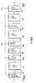
- Fig. 1 is a block diagram of a pipeline type digital signal processing device conventionally used.
- reference numbers 1, 3, and 5 designate unit circuits
- a reference number 7 denotes an input register
- a reference number 13 is an output register
- reference numbers 9 and 11 are registers.
- the unit circuits 1, 3, and 5 are connected to one another through the input register 7, the output register 13, and the other registers 9 and 11 in series.
- the unit circuits 1, 3, and 5 are stages of the pipeline type digital signal processing device. This way, a circuit block having a certain function in the conventional digital signal processing device is divided into the many stages such as the circuit units 1, 3, and 5, and the registers 9 or 11 is located between the unit 1, 3, or 5 so as to reduce the cycle time of the digital signal processing device.
- a delay time of each stage in the digital signal processing device is so equal to one another that the total cycle time of the digital signal processing device can be reduced approximately one third (1/3) times of a digital signal processing device which is not a pipeline type.
- a circuit block in the digital signal processing device is divided into a plurality of stages each of which has a certain function, for example an arithmetic and logic unit (ALU) with a longer delay time or an unit for a writing operation for a register with a shorter delay time as the function.
- ALU arithmetic and logic unit
- the magnitude of the entire cycle time of the pipeline type digital signal processing device is determined by the stage having the largest delay time. Accordingly, whenever the delay time of the stages other than the stage having the largest delay time may be reduced, the magnitude of the entire delay time is never decreased.
- the delay time of each stage should be equaled to one another or the number of stages obtained by dividing the circuit block may be increased so that there is the problem in which it is difficult and complex so as to execute a recover operation when the pipeline hazard is caused by a branch, a trap, an exception or the other operations.
- an object of the present invention is to provide an improved pipeline type digital signal processing device which can reduce an entire cycle time thereof without increasing a new stage.
- a pipeline type digital signal processing device having a plurality of pipeline stages in which at least one of the stages comprises a first unit circuit, a second unit circuit located at a rear portion of the first unit circuit, a first latch means located between the first unit circuit and the second unit circuit, and a second latch means installed between the second unit circuit and next stage and an output of the first latch means is given to the second unit circuit, wherein an output of the second unit circuit is applied to the second latch means, an operation of the first latch means is controlled by a first clock signal and an operation of the second latch means is controlled by a second clock signal which is a reversed clock signal as a reversed phase of the first clock signal.
- the maximum delay time of the second unit circuit is shorter than that of the first unit circuit.
- this invention can be applied to the stage having the maximum delay time in a pipeline type digital signal processing device.
- the stage is divided into the first and second unit circuits and the first latch means is provided between these unit circuits and the second latch means is located between the second unit circuit and the next stage.
- These latch means are controlled by the first and second clock signals which are in reverse each other. Accordingly, when one of the latch means is in a through state or in an active state, the other is in locked state or in an inactive state. Namely, the two latch means can not be in the through state at the same time.
- the first unit circuit is executed in one cycle step and then the second unit circuit is operated in the next cycle step.
- the operations of the first and second unit circuits are so controlled based on the first and second clock signals which are in reverse each other that faulty operations never occur.
- the present invention is applied to the digital signal processing device having stages, for example the delay time of one of the stages is changed by an operational condition, as the delay time of each stage of the digital signal processing device can be uniformed.
- Fig. 2 is a block diagram of a pipeline type digital signal processing device based on a master-slave latch type as a first embodiment according to the present invention.
- a circuit block comprises an unit circuit 20, a first unit circuit 22a, a second unit circuit 22b, and an unit circuit 24.
- the unit circuit 3 as the stage 3 of the conventional digital signal processing device as shown in Fig. 1 is divided into the first unit circuit 22a and the second unit circuit 22b in the present embodiment.
- the unit circuits 22, 22a, 22b, and 24 are connected to one another in series through an input register 26, a register 28, a master latch 30a as a first latch means, a slave latch 30b as a second latch means, and an output register 32.
- the master latch 30a and the slave latch 30b are made up of a transparent latch as shown in Fig. 4 showing a circuit diagram of the transparent latch formed with CMOS circuits.
- a clock signal (CLK) is applied to the input register 26, the register 28, the slave latch 30b, and the output register 32 so as to execute them under the same condition.
- an inverted clock ( CLK ) of the clock signal (CLK) is given to the master latch 30a.
- the master latch 30a is transparent, the operation of the slave latch 30b is locked.
- the slave latch is transparent, namely in the through state.
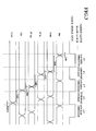
- Fig. 3 shows a timing chart so as to explain the operation of the digital signal processing device of the first embodiment as shown in Fig. 2.
- a data flow of the circuit 22a through the unit circuit 24 is explained after the data IN is given to the unit circuit 20 as the first stage of the digital signal processing device, then to the unit circuit 22a as the next stage thereof.
- the unit circuit 22a inputs data Bin. After the unit circuit 22a obtains the data Bin and then a delay time Td,B of it is passed, an output of the unit circuit 22b is determined. At this time, the clock signal CLK is in the latter denoted by ⁇ 2 of the cycle.
- the master latch 30a is in the through state so that the output Bout of the unit circuit 22a is given to the input B'in of the circuit unit 22b after an propagation delat, Tdr of the master latch 30a.
- the unit circuit 22b outputs the valid B'out.
- the master latch 30a is in the lock state.
- the slave latch 30b is in the through state.
- the output B'out is given to an input Cin of the unit circuit 24 through the slave latch 30b. After the delay time Td,c of the unit circuit 24, the output Cout is obtained.
- Tcycle Td,B + Td,B' + Td,C + 3Tdr + Tsetup.
- the total cycle time Tcycle conv. is:
- the cycle time of the first embodiment is one third Td times (1/2Td) as short as that of the conventional digital signal processing device.
- the pipeline type digital signal processing device can reduce the cycle time approximately 25 % compared with that of the conventional digital signal processing device.
- a part of the maximum delay time can be shifted into the next cycle, such as ⁇ 3 shown in Fig. 3, so as to reduce the total cycle time of the digital signal processing device.
- Fig. 5 is a timing chart of a digital signal processing device as the first embodiment according to the present invention having a relatively longer cycle time ( ⁇ 1 ⁇ ⁇ 1') compared to the cycle time as shown in Fig. 3.
- a structure of the digital signal processing device of this embodiment such as stages is same as that of the first embodiment. Only the cycle time is different each other. In one cycle, for instance in a cycle ⁇ 1', the input data never flow through the unit circuit 22a, the master latch 30a, the unit circuit 22b, and the slave latch 30b even if the period of one cycle is longer than that of the first embodiment.
- the input data flows in synchronization with the clock signal so that faulty operation of each stage can be eliminated in the digital signal processing device according to the present embodiment even if the period of the cycle time is longer than that of the device of the first embodiment.
- the operations of the digital signal processing device are executed in the period of the cycle time equal to that of the conventional digital signal processing device as shown in Fig. 1.
- the present invention can be reduced to the total operation time of the pipeline type digital signal processing device.
- Fig. 6 is a block diagram of a pipeline type digital signal processing device as a second embodiment according to the present invention.
- a part E'out of an output of a second stage 52 is given into an unit circuit 53, a master latch 54 is installed in a front portion of the circuit unit 53, and a slave latch 55 is provided in a rear portion of the unit circuit 53.
- a clock signal is applied into an input register 57, a register 58, the slave latch 55, and an output register 59. While, a reversed clock signal as a reversed phase of the clock signal is given into the master latch 54.
- the unit circuit 53 based on the present embodiment so that the unit circuit to be divided can be constructed on a small size.
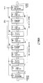
- Fig. 7 is a block diagram of a digital signal processing device of a third embodiment according to the present invention.
- the master slave latch structure as the present invention is applied to the first stage 61 and the second stage as the next stage.
- the first stage comprises an unit circuit 68, a master latch 64, an unit circuit 69, and a slave latch 65.
- the master latch is incorporated between the unit circuits 68 and 69.
- the slave latch 65 is provided between the unit circuit 69 and the second stage 62.
- the second stage is made up of a circuit unit 70, a master latch 66, an unit circuit 71, and a slave latch 67.
- the master latch is provided between the circuit units 70 and 71.
- the slave latch 67 is incorporated at the rear portion of the unit circuit 71.
- the master latches 64 and 66 of the first and second stages are executed by the clock signal, on the other hand, the slave latches 65 and 67 are operated by a reversed clock signal as a reversed phase of the clock signal.
- the delay time of each stage is so equal to each other that the delay time of the digital signal processing device of the first embodiment as shown in Fig. 1 can further be reduced by the present embodiment.
- the structure of the present embodiment can be most applied to the case that a delay time of a stage of a pipeline type digital signal processing device is changed by an instruction and a kind of data.
Landscapes
- Engineering & Computer Science (AREA)
- Software Systems (AREA)
- Theoretical Computer Science (AREA)
- Physics & Mathematics (AREA)
- General Engineering & Computer Science (AREA)
- General Physics & Mathematics (AREA)
- Advance Control (AREA)
- Image Processing (AREA)
- Complex Calculations (AREA)
Applications Claiming Priority (2)
| Application Number | Priority Date | Filing Date | Title |
|---|---|---|---|
| JP6383/90 | 1990-01-17 | ||
| JP2006383A JPH03211613A (ja) | 1990-01-17 | 1990-01-17 | ディジタル信号処理装置 |
Publications (2)
| Publication Number | Publication Date |
|---|---|
| EP0438126A2 true EP0438126A2 (fr) | 1991-07-24 |
| EP0438126A3 EP0438126A3 (en) | 1993-06-30 |
Family
ID=11636864
Family Applications (1)
| Application Number | Title | Priority Date | Filing Date |
|---|---|---|---|
| EP19910100433 Withdrawn EP0438126A3 (en) | 1990-01-17 | 1991-01-16 | Pipeline type digital signal processing device |
Country Status (3)
| Country | Link |
|---|---|
| EP (1) | EP0438126A3 (fr) |
| JP (1) | JPH03211613A (fr) |
| KR (1) | KR940001556B1 (fr) |
Cited By (4)
| Publication number | Priority date | Publication date | Assignee | Title |
|---|---|---|---|---|
| FR2770661A1 (fr) * | 1997-11-03 | 1999-05-07 | Inside Technologies | Microprocesseur comprenant des moyens de concatenation de bits |
| FR2770660A1 (fr) * | 1997-11-03 | 1999-05-07 | Inside Technologies | Microprocesseur, notamment pour carte a puce |
| EP0877315A3 (fr) * | 1997-03-14 | 2002-02-13 | Nokia Mobile Phones Ltd. | Circuit à traitement de données |
| CN101232360B (zh) * | 2007-01-23 | 2011-08-10 | 华为技术有限公司 | 数据接收装置及方法 |
Families Citing this family (1)
| Publication number | Priority date | Publication date | Assignee | Title |
|---|---|---|---|---|
| KR100452174B1 (ko) * | 1995-06-27 | 2005-01-05 | 코닌클리케 필립스 일렉트로닉스 엔.브이. | 파이프라인데이터처리회로 |
Family Cites Families (3)
| Publication number | Priority date | Publication date | Assignee | Title |
|---|---|---|---|---|
| DE3166256D1 (en) * | 1981-03-23 | 1984-10-31 | Ibm Deutschland | Device for shortening the cycle time in a data processing device |
| CA1302585C (fr) * | 1987-04-10 | 1992-06-02 | Brian Lefsky | Technique anti-dephasage pour processeur pipeline |
| JPH01255036A (ja) * | 1988-04-04 | 1989-10-11 | Toshiba Corp | マイクロプロセッサ |
-
1990
- 1990-01-17 JP JP2006383A patent/JPH03211613A/ja active Pending
-
1991
- 1991-01-15 KR KR1019910000510A patent/KR940001556B1/ko not_active Expired - Lifetime
- 1991-01-16 EP EP19910100433 patent/EP0438126A3/en not_active Withdrawn
Cited By (8)
| Publication number | Priority date | Publication date | Assignee | Title |
|---|---|---|---|---|
| EP0877315A3 (fr) * | 1997-03-14 | 2002-02-13 | Nokia Mobile Phones Ltd. | Circuit à traitement de données |
| FR2770661A1 (fr) * | 1997-11-03 | 1999-05-07 | Inside Technologies | Microprocesseur comprenant des moyens de concatenation de bits |
| FR2770660A1 (fr) * | 1997-11-03 | 1999-05-07 | Inside Technologies | Microprocesseur, notamment pour carte a puce |
| WO1999023552A1 (fr) * | 1997-11-03 | 1999-05-14 | Inside Technologies | Microprocesseur, notamment pour carte a puce |
| WO1999023550A1 (fr) * | 1997-11-03 | 1999-05-14 | Inside Technologies | Microprocesseur comprenant des moyens de concatenation de bits |
| US6317825B1 (en) | 1997-11-03 | 2001-11-13 | Inside Technologies | Microprocessor comprising bit concatenation means |
| US6779105B1 (en) | 1997-11-03 | 2004-08-17 | Inside Technologies | Two pipeline stage microprocessor and method for processing an instruction |
| CN101232360B (zh) * | 2007-01-23 | 2011-08-10 | 华为技术有限公司 | 数据接收装置及方法 |
Also Published As
| Publication number | Publication date |
|---|---|
| JPH03211613A (ja) | 1991-09-17 |
| EP0438126A3 (en) | 1993-06-30 |
| KR940001556B1 (ko) | 1994-02-24 |
| KR910014805A (ko) | 1991-08-31 |
Similar Documents
| Publication | Publication Date | Title |
|---|---|---|
| JP2735034B2 (ja) | クロック信号分配回路 | |
| EP0102242B1 (fr) | Appareil de traitement de données | |
| KR100304036B1 (ko) | 데이타동기시스템및방법 | |
| US4999802A (en) | Floating point arithmetic two cycle data flow | |
| EP0080836A2 (fr) | Circuit monolithique digital à temps discret de convolution | |
| US11740651B2 (en) | Clock multiplexer device and clock switching method | |
| US4961013A (en) | Apparatus for generation of scan control signals for initialization and diagnosis of circuitry in a computer | |
| US5257214A (en) | Qualification of register file write enables using self-timed floating point exception flags | |
| GB2079998A (en) | Frequency-dividing circuit | |
| EP0136174B1 (fr) | Hardware de test d'unité arithmétique-logique | |
| EP0438126A2 (fr) | Dispositif de traitement de signaux numériques de type pipeline | |
| KR870009595A (ko) | 직렬-비트 2의 보수 디지탈 신호 처리 장치 | |
| US20240077906A1 (en) | Processor and computing system | |
| EP0278529A2 (fr) | Circuit de multiplication capable d'opérer à haute vitesse avec peu de matériel | |
| US6434588B1 (en) | Binary counter with low power consumption | |
| US6185720B1 (en) | Slaveless synchronous system design | |
| US4677584A (en) | Data processing system with an arithmetic logic unit having improved carry look ahead | |
| US7047392B2 (en) | Data processing apparatus and method for controlling staged multi-pipeline processing | |
| US6057720A (en) | High speed sticky signal generator | |
| US5018092A (en) | Stack-type arithmetic circuit | |
| US20230214180A1 (en) | Using and/or reduce carry chains on programmable hardware | |
| US5598552A (en) | Error free data transfers | |
| JP4428819B2 (ja) | 多入力データソーティング回路 | |
| US6910122B1 (en) | Method and apparatus for preserving pipeline data during a pipeline stall and for recovering from the pipeline stall | |
| US6856172B1 (en) | Sequential logic circuit for frequency division |
Legal Events
| Date | Code | Title | Description |
|---|---|---|---|
| PUAI | Public reference made under article 153(3) epc to a published international application that has entered the european phase |
Free format text: ORIGINAL CODE: 0009012 |
|
| 17P | Request for examination filed |
Effective date: 19910116 |
|
| AK | Designated contracting states |
Kind code of ref document: A2 Designated state(s): DE FR GB |
|
| PUAL | Search report despatched |
Free format text: ORIGINAL CODE: 0009013 |
|
| AK | Designated contracting states |
Kind code of ref document: A3 Designated state(s): DE FR GB |
|
| STAA | Information on the status of an ep patent application or granted ep patent |
Free format text: STATUS: THE APPLICATION IS DEEMED TO BE WITHDRAWN |
|
| 18D | Application deemed to be withdrawn |
Effective date: 19950801 |