EP0438273A2 - Halbleiterspeichergeräte mit Spaltenredundanz - Google Patents
Halbleiterspeichergeräte mit Spaltenredundanz Download PDFInfo
- Publication number
- EP0438273A2 EP0438273A2 EP91300295A EP91300295A EP0438273A2 EP 0438273 A2 EP0438273 A2 EP 0438273A2 EP 91300295 A EP91300295 A EP 91300295A EP 91300295 A EP91300295 A EP 91300295A EP 0438273 A2 EP0438273 A2 EP 0438273A2
- Authority
- EP
- European Patent Office
- Prior art keywords
- data
- register
- flop
- column
- flip
- Prior art date
- Legal status (The legal status is an assumption and is not a legal conclusion. Google has not performed a legal analysis and makes no representation as to the accuracy of the status listed.)
- Granted
Links
Images


Classifications
-
- G—PHYSICS
- G11—INFORMATION STORAGE
- G11C—STATIC STORES
- G11C29/00—Checking stores for correct operation ; Subsequent repair; Testing stores during standby or offline operation
- G11C29/70—Masking faults in memories by using spares or by reconfiguring
- G11C29/78—Masking faults in memories by using spares or by reconfiguring using programmable devices
- G11C29/84—Masking faults in memories by using spares or by reconfiguring using programmable devices with improved access time or stability
- G11C29/846—Masking faults in memories by using spares or by reconfiguring using programmable devices with improved access time or stability by choosing redundant lines at an output stage
Definitions
- This invention relates to semiconductor memory devices having column redundancy. Such devices may for example be used as video memories in which data are inputted and outputted serially, and the data are converted into or from parallel data therein.
- a video memory such as a field memory has a memory cell array composed of DRAM type cells and performs serial-parallel conversion and parallel-serial conversion during writing and reading, respectively, by means of a register, for inputting or outputting the serial data.
- the column decoder is dispensed with in a video memory because one-row data are written or read out collectively to or from the memory cell array. Therefore, if the defective memory cell column is exchanged in the redundancy circuit, since the addresses cannot be specified directly to the redundancy circuit, it becomes necessary to add various circuits.
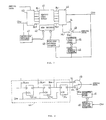
- Figure 1 shows portions of an example of a previously proposed memory device having a column redundant section.
- a read shift register 102 and a write shift register 103 are provided in a RAM section 101 having a memory cell array for data storage.
- data are transmitted in parallel from the RAM section 101, and thence outputted serially.
- Data are inputted serially in the write shift register 103 and transferred in parallel to the RAM section 101.
- the RAM section 101 and a column redundant section 104 provided thereat are associated with a row decoder 105 to effect row selection.
- the column redundant section 104 rescues column defects in the RAM section 101 by row-by-row substitution, and data to be stored intrinsically in the column defective portion are stored in the column redundant section 104.
- the video memory device is provided with a fuse ROM 110 for storing column-defective column data (column address), a write address comparator circuit 111W, a read addresses comparator circuit 111R, a write switching circuit 112W, a read switching circuit 112R, a write redundancy latch 113W and a read redundancy latch 113R.
- a write address comparator circuit 111W a read addresses comparator circuit 111R
- a write switching circuit 112W a read switching circuit 112R
- a write redundancy latch 113W a read redundancy latch 113R
- the fuse ROM 110 the comparator circuits 111R and 111W, and the switching circuits 112W and 112R are required for controlling the column redundant section 104, so that a corresponding area on the chip has been required.
- the read-out erroneous data are replaced by the redundant data by the switching circuit 112R with consumption of excess time.
- a semiconductor memory device for storing video data, the device comprising: a memory cell array including a plurality of memory cells arrayed in a matrix; a register including a plurality of serially connected flip-flops for shifting data therein, said register being capable of inputting or outputting data in parallel from or to said memory cell array and also being capable of outputting or inputting data in series to or from the outside of the device; a column redundant section for storing data in lieu of a defective column of said memory cell array, said column redundant section being provided adjoining said memory cell array, the cells of said column redundant section and of said memory cell array being commonly selected by each of word lines; a redundant latch section associated with said column redundant section for holding the data from said register transiently; and control means for storing erroneous bit data of said defective column and for generating a control signal to control said register; wherein the data in said register are transferred in idle at said flip-flop relevant to said defective column by said control signal supplied from said control means.
- a semiconductor memory device for storing video data, the device comprising: a memory cell array including a plurality of memory cells arrayed in a matrix; a read register capable of inputting data in parallel from said memory cell array and of outputting data in series; wherein erroneous data of a defective column of said memory cell array are replaced by correlative data at said read register.
- a semiconductor memory device comprises a register containing a plurality of serially connected flip-flops, the register being capable of inputting and outputting data in parallel to or from an array of memory cells and also being capable of inputting and outputting data in series to or from the outside of the chip.
- the memory device includes a redundant column section, and a redundant latch section associated with the redundant column section, and data are transferred in idle in the flip-flop circuit of the register associated with the memory cell column having an erroneous bit. The transferring in idle or the passing of the data is controlled by an erroneous bit data storage circuit in which the column data of the erroneous bits are stored.
- a memory device handling video data wherein on the basis of signals from erroneous bit data storage means storing the column data of the erroneous bits, the erroneous bits read out from the memory cell are read after replacement by correlative data bits.
- the correlative data bits may be enumerated by, for example, data bits one bit before, data bits one bit after, data bits one field before, or data bits one frame after.
- Embodiments of memory device according to the present invention have a general construction as shown in Figure 2 for rescuing column defects.
- the memory device includes a memory cell array 1 having DRAM type cells, the memory cells being arrayed in a matrix configuration in the memory cell array 1.
- the number of columns of the memory cells is (N+1), where N is an integer.
- the end column of these (N+1) columns is a column redundant section 5 for rescuing column defects.
- a plurality of word lines WL are provided for row selection in the memory cell array 1, these word lines being formed in a parallel pattern at the gates of access transistors, not shown, of the memory cells.
- the word lines WL are connected to a row decoder 2 which raises the potential of the word line WL to be selected in accordance with address signals.
- the memory cell array 1 is also provided with a plurality of bit lines BL1, ..., BL N+1 extending in parallel with one another in a direction normal to the word lines WL. These bit lines are used to effect data read-out.
- the bit lines BL1, ..., BL N+1 are connected to capacitances in the memory cells by means of access transistors so that their voltages are amplified by sensing amplifiers, not shown.
- the number of bit lines is (N+1).
- the number of redundant bit lines need not be one, but may be more, in which case a number of column-defective memory cell columns corresponding to the number of redundant bit lines may be replaced.
- the bit lines BL1, ..., BL N+1 are connected to the read shift register 3 and the write shift register 4.
- the read shift register 3 is used for outputting the parallel data from the bit lines BL1, ..., BL N+1 after conversion thereof into serial data.
- the read shift register 3 is composed of (N+1) series connected flip-flop circuits, the end part of which is a redundant latch section 6 for latching data from the column redundant section 5.
- the write shift register 4 is used for converting serial data from outside into parallel data, and writing the converted data into memory cells by means of the bit lines BL1, ..., BL N+1 .
- the write shift register 4 is similarly composed of (N+1) serially connected flip-flop circuits, the end part of which is a redundant latch section 7 for latching data to be transferred to the column redundant section 5.
- the memory device includes a fuse ROM 8 forming erroneous bit data storage means for storing column data for defective bits, that is the defective column address.
- the fuse ROM 8 is a circuit for storage of address signals by the pattern of fuse connection and disconnection of the previously melted fuse or fuses, such that, if the column with a column address x is defective, as indicated by hatching in Figure 2, a signal to the effect that the column of the x′th address is in error is outputted from the fuse ROM 8.
- the shift register is so arranged and constructed that a forward stage D-flip-flop and a rear stage D-flip-flop are associated with each bit line.
- Inverters In1 to In8 are arranged to form the D-flip-flops. That is, a set of inverters In1 and In2, a set of inverters In3 and In4, a set of inverters In5 and In6, and a set of inverters In7 and In8 have their input terminals connected to the output terminals to form the flip-flops. Between the adjoining flip-flops, there are provided CMOS switch type transfer gates formed by pMOS transistors 11 to 14 and nMOS transistors 19 to 22.
- CMOS switch type transfer gates which are formed by pMOS transistors 15 to 18 and nMOS transistors 23 to 26.
- bit lines BL x and BL x+1 To the input side of the forward stage flip-flop are connected bit lines BL x and BL x+1 by means of pMOS transistors 27 and 28 functioning as switches.
- the register operation differs between the flip-flop for the bit line BL x of the memory cell column where column defects have occurred and the flip-flop for the bit line BL x+1 of the memory cell column performing normal operation. Above all, idle transfer or passing occurs in the flip-flop of the bit line BL x .
- Figure 4 shows a signal generator for actuating the transistors 11 to 26.
- the fuse ROM 8 generates a signal f R which is to be supplied to the flip-flop of the bit line BL x of the memory cell column where column defects have occurred, while generating a signal f N which is to be supplied to the flip-flop of the bit line BL x+1 of the memory cell column performing a normal operation.
- the signal f R is always at an "H" (high) level and is, in effect, a defective column address signal.
- the signal f N is always at an "L" (low) level and is supplied to all of the regular memory cell columns other than the bit line BL x .
- the signals f R and f N are supplied to NOR gates 30 and 31, to the other input terminals of which a clock signal ⁇ CK alternating between the "H" level and the "L” level at a constant period.
- the output of the NOR gate 30, supplied with the signal f R is always a signal ⁇ R at the "L” level
- the output of the NOR gate 31, supplied with the signal f N is always a signal ⁇ N inverted relative to the clock signal ⁇ CK .
- the signal f N which is always at the "L” level is supplied to the gate of the transistor 28 between the bit line BL x+1 , so that the transistor 28 is always turned on.
- the signal ⁇ CK is supplied to the gate of the transistor 13 ahead of the forward stage flip-flop, while the signal ⁇ N is supplied to the gate of the transistor 21 so that, when the signal ⁇ CK is at the "L" level, this CMOS switch is turned on.
- the inverter In5 generates an inverted output
- the inverter In6 generates an inverted output of said inverted output.
- the transistors 14 and 17 and the transistors 22 and 25 are all turned off so that the data are not latched.
- the transistor 17 and the transistor 25 are turned on, while the transistor 13 and the transistor 21 are turned off, so that the data are latched.
- the transistor 14 and the transistor 22 are turned on, so that data are transferred from the forward stage flip-flop to the rear stage flip-flop, and the output of the inverter In7 is at the same level as the input of the inverter In5.
- the signal ⁇ CK falls from the "H" level to the "L” level and the rear stage D-flip-flop is latched by means of the MOS transistors 18 and 26, at the same time that the transistors 14 and 22, acting as switches between the forward stage and the rear stage, are turned off, while the transistors 13 and 21, acting as the transfer gates at the input side of the forward stage flip-flop are turned on. Data are transferred by the above described cyclic operation. Meanwhile, the operation of the flip-flop corresponding to the normal memory cell is the same as that of a known shift register.
- the idle transfer operation of the flip-flop associated with the bit line BL x of the memory cell column suffering from column defects is hereinafter explained.
- the signal f R which is always at the "H” level is supplied to the gate of the transistor 27 between the bit line BL x and the flip-flop, so that the transistor 27 is always turned off. This is tantamount to the bit line BL x with the defective column being disconnected.
- the flip-flop, transferring in idleness, should intrinsically be supplied with the signal ⁇ N , is supplied with the signal ⁇ R which is always at the "L" level, so that it performs an idle transfer operation without data latching.
- the transistors 19 and 24 are always turned off, while the transistors 12 and 15 are always turned on. Since the transistor 12 is always turned on, the signal supplied to the inverter In1 directly appears at the output of the inverter In3, without regard to the level of the signal ⁇ CK . Thus the data are always latched in the forward stage flip-flop and data are transmitted to the output of the inverter In3 when the transistor 11 is turned on.
- idle transfer may be made between the redundant latch sections 6 and 7.
- one memory cell column with the defective column is replaced by one column, this is not limitative and a plurality of columns of column redundant sections may be provided to cope with several defective columns.
- the number of shift registers is not limited to one for each of the read and write shift register.
- the second embodiment to be described is a modification of the first embodiment, in which the signal to be supplied to the transfer gate of the shift register is modified.
- the circuit construction of the shift register shown in Figure 5 is the same as the circuit construction shown in Figure 3 except that the pMOS transistors 27 and 28 are changed to nMOS transistors 34 and 35.
- the same reference numerals are used, and detailed description is omitted.
- a fuse ROM 8 generates a signal f N which is always “H” to the normal memory cell column, while generating a signal f R which is always “L” to the defective memory cell column.
- This signal f R is to be the defective column address signal.
- These signals are supplied to NAND gates 32 and 33.
- a clock signal ⁇ CK is also supplied to the other input terminals of the NAND gates 32 and 33. This clock signal ⁇ CK as a signal alternating between the "H” level and the "L” level at a constant period.
- the output of the NAND gate 33 supplied with the signal f N which as always at the "H” level, is a signal ⁇ n which is inverted from the clock signal ⁇ CK .
- the output of the NAND gate 32 supplied with the signal f R which as always at the “L” level, is a signal ⁇ r which, irrespective of the clock signal ⁇ CK , is always at the "H” level.
- the circuit construction of the present embodiment is such that latching occurs with falling of the clock signal ⁇ CK , and control is made by the clock signal ⁇ CK and the signals ⁇ r and ⁇ n generated at the NAND gates 32 and 33.
- the nMOS transistor 20 between the forward and rear stages of the D-flip-flop associated with the defective memory cell column is always turned on by the signal ⁇ r .
- the data are not latched by, but passed through the nMOS transistor through which the data is transferred in idleness.
- the circuitry for switching control such as switching circuits or address comparators, may be eliminated to save chip area. Since the control circuits are unnecessary, high-speed read-out is also enabled.
- FIG. 7 shows a third embodiment applied to a video memory device in which defective bits are replaced by correlated data bits.
- This memory device includes a memory cell array 41 having memory cells in a matrix configuration. In each memory cell of the memory cell array 41, there are stored video data, such as TV signals. In this memory cell array 41 are formed row-selecting word lines, not shown, each word line being selected by a row decoder 42.
- N bit lines BL1 to BL N are formed at right angles to and in parallel with one another. These bit lines BL1 and BL N are connected to both a write shift register 43 and a read shift register 44.
- the write shift register 43 is a register for converting serial data from outside into parallel data for transfer thereof to the memory cell array 41.
- a write clock signal CK W is supplied to the write shift register 43.
- the read shift register 44 is a register for converting the parallel data from the memory cell array 41 into serial data and reading out the serial data by means of a read-out line ML.
- a read clock signal CK R is supplied to the read shift register 44.
- the read shift register 44 is provided with wiring SL for substitution by data one bit after, and the erroneous data may be replaced by a data bit which is transmitted over the wiring SL.
- the write clock signal CK W is supplied to both the write shift register 43 and a write row address counter circuit 47.
- the write row address counter circuit 47 counts the clocks of the write clock signal CK W and transmits the signal of the row address related with writing to the row decoder 42.
- the read clock signal CK R is supplied to the read shift register 44, while being supplied to both a read row address counter circuit 48 and a data substitution counter circuit 46.
- the read row address counter 48 counts the clocks of the read clock signals CK R to transmit the signal of the row address pertaining to reading to the row decoder 42. Since the present memory device is a video memory, address signals such as those of RAMs in general are not supplied, but row addresses are generated by the respective clock signals CK W and CK R .
- the above described data-substituting counter circuit 46 is a circuit generating column addresses and, as it were, a circuit for counting the data shift state in the read shift register 44.
- the column addresses generated in the data-substituting counter circuit 46 are transmitted to an address comparator fuse circuit 45.
- the address comparator fuse circuit 45 includes a fuse ROM in which addresses for erroneous bits are stored in advance by the fuse melting pattern.
- the address comparator fuse circuit 45 also compares column addresses supplied from the data-substituting counter circuit 46, and the addresses of the erroneous bits from the fuse ROM. If the addresses coincide, a pulse of a signal ⁇ ID is generated.
- the signal ⁇ ID controls the switching of a switch 49.
- the switch 49 is a changeover switch for selecting if the serial data to be outputted should be taken from the wiring SL or from the reading line ML. Usually, the data from the reading line ML are transmitted to outside. However, if the pulse from the address comparator fuse circuit 45 is generated in the signal ⁇ 1D, the switch 49 is switched to the side of the wiring SL. As a result, the erroneous bit is replaced by a data bit which is one bit later.
- Figure 8 shows the terminal portion of the read shift register 44 of the memory device of the present embodiment and its peripheral circuit.
- the read shift register 44 includes flip-flops DF N-2 , DF N-1 and DF N which are connected in series in its terminal portion.
- the bit line BL N-2 is connected to the D-terminal of the flip-flop DF N-2
- the bit line BL N-1 is connected to the D-terminal of the flip-flop DF N-1
- the bit line BL N is connected to the D-terminal of the flip-flop DF N .
- Read clock signals CK R are supplied to clock input terminals of the flip-flops DF N-2 , DF N-1 and DF N .
- the Q-terminal of the final stage flip-flop DF N is to be the read-out line ML and reading to outside is switchingly controlled by the switch 49.
- the wiring SL is taken out from the D-terminal of the final stage flip-flop DF N , that is, the Q-terminal of the preceding flip-flop DF N-1 . From the wiring SL, the next succeeding bit data are taken out without the intermediary of the final stage flip-flop DF N .
- the wiring SL is also switched by the switch 49 so that the next succeeding bit data is outputted by means of the wiring SL only on occurrence of the pulse of the signal ⁇ ID .
- the data bit appearing at the Q-terminal of the flip-flop DF N-1 of the preceding stage of the final stage is outputted at an output line without the intermediary of the last stage flip-flop DF N , so that the erroneous bit is not outputted.
- the data preceding the current data by one bit exhibits similarity because the video signals show correlation. Hence, when the image is viewed on a monitor, such substitution is not noticed by the human eye.
- the output line of the switch 49 is switched by the signal ⁇ ID from the wiring SL to the read-out line ML so that the usal data shift operation is continued.
- the feature that video data is correlated is utilised for replacing the erroneous bit by the directly succeeding data bit.
- the erroneous bit may be prevented from being outputted without providing a control system for redundant column or write side redundant circuits.
- the defective columns can be rescued without increasing chip area.
- any suitable circuit construction may be used for the switch 49, if it is a semiconductor circuit provided on one and the same chip.
- the fourth embodiment is a modification of the third embodiment and is an example in which read clock signals CK R are interrupted.
- the present embodiment differs from the third embodiment in that the read clock signal CK R inputted to the last stage flip-flop DF N is interrupted transiently without latching the erroneous data and without substituting the bit of the flip-flop DF N-1 of the stage preceding the final stage by the switch 49.
- the read shift register 44 of the present embodiment is so formed that a switch 50 is provided at a clock input terminal CK of the final stage flip-flop DF N , the read clock signals CK R are supplied to the final stage flip-flop DF N on closure of the switch 50, and the read clock signals CK R are not supplied to the final stage flip-flop DF N on opening of the switch 50.
- the switch 50 is controlled by the signal ⁇ ID generated by the address comparator fuse circuit 45 and the data substitution counter circuit 46 is similar to that of the third embodiment.
- the erroneous bit replacing operation in the memory device of the fourth embodiment will be explained briefly.
- the switch 50 is normally closed and the bits are sequentially shifted in accordance with the clocks of the read clock signals CK R .
- the pulse of the signal ⁇ ID is generated from the address comparator fuse circuit 45 to open the switch 50.
- the last stage flip-flop DF N then ceases latching the data and the data outputted as the serial data are the same as the preceding bit.
- the erroneous bit is not outputted, but is replaced by a one-bit preceding data which shows correlation with it.
- the switch 50 is again closed by the signal ⁇ ID , so that the last stage flip-flop DF N is returned to the data-latching stage.
- the feature of image data having intrinsic image correlation is utilised for replacing the erroneous bit by the directly preceding bit.
- the erroneous bit may be prevented from being outputted without providing the redundant column or a control system for the write side redundant circuit.
- the column defects can be remedied without increasing chip area.
- the fifth embodiment is similarly a modification of the third embodiment in which a latch circuit is associated with the final stage shift register.
- This embodiment differs from the third embodiment in that a flip-flop DF EX is provided next to the final stage flip-flop DF N for storing one-bit-preceding data and, when the erroneous bit is about to be outputted, the output is switched to the side of the flip-flop DF EX by the switch 51, without replacement by the bit of the last but one flip-flop DF N-1 .
- the read shift register 44 of the memory device of the present embodiment includes a flip-flop DF EX having its D-terminal connected to the Q-terminal of the final stage flip-flop DF N .
- the Q-terminal of the flip-flop DF EX may be selected by a switch 51.
- the read clock signal CK R is supplied to the flip-flop DF EX , similarly to other flip-flops.
- the switch 51 is provided for selectively outputting the output of the final stage flip-flop DF N or the output of the flip-flop DG EX and is controlled by a signal ⁇ ID .
- the address comparator fuse circuit 45 for generating the signal ⁇ ID or the data substitution counter circuit 46 are constructed similarly to those described previously.
- data of the Q-terminal of the final stage flip-flop DF N is outputted by means of the switch 51.
- the annexed flip-flop DF EX is operating for permanently storing the bit preceding the current bit by one bit.
- the switch 51 When replacing the erroneous bit, the switch 51 is switched to the side of the annexed flip-flop DF EX at the timing of appearance of the erroneous bit at the Q-terminal of the final stage flip-flop DF N .
- the switch 51 is switched to the side of the annexed flip-flop DF EX at the timing of appearance of the erroneous bit at the Q-terminal of the final stage flip-flop DF N .
- correlation in the video data is utilised for replacing the erroneous bit by the immediately preceding data bit.
- the erroneous bit may be prevented from being outputted without providing the redundant column or the control system for the redundant circuit on the write side.
- the defective column may be rescued without increasing chip area.
- the erroneous bit is replaced by the directly succeeding bit data or the directly preceding bit data in the third to fifth embodiments, the erroneous bit may also be replaced by bits of a directly preceding line, field or frame, by taking advantage of the correlation in the video signals.
Landscapes
- For Increasing The Reliability Of Semiconductor Memories (AREA)
- Dram (AREA)
- Techniques For Improving Reliability Of Storages (AREA)
Applications Claiming Priority (2)
| Application Number | Priority Date | Filing Date | Title |
|---|---|---|---|
| JP2009104A JPH03214500A (ja) | 1990-01-18 | 1990-01-18 | メモリ装置 |
| JP9104/90 | 1990-01-18 |
Publications (3)
| Publication Number | Publication Date |
|---|---|
| EP0438273A2 true EP0438273A2 (de) | 1991-07-24 |
| EP0438273A3 EP0438273A3 (en) | 1992-05-13 |
| EP0438273B1 EP0438273B1 (de) | 1996-09-11 |
Family
ID=11711323
Family Applications (1)
| Application Number | Title | Priority Date | Filing Date |
|---|---|---|---|
| EP91300295A Expired - Lifetime EP0438273B1 (de) | 1990-01-18 | 1991-01-16 | Halbleiterspeichergeräte mit Spaltenredundanz |
Country Status (4)
| Country | Link |
|---|---|
| US (1) | US5231604A (de) |
| EP (1) | EP0438273B1 (de) |
| JP (1) | JPH03214500A (de) |
| DE (1) | DE69121921T2 (de) |
Families Citing this family (24)
| Publication number | Priority date | Publication date | Assignee | Title |
|---|---|---|---|---|
| JP2796590B2 (ja) * | 1991-08-07 | 1998-09-10 | 三菱電機株式会社 | メモリ装置及びそれを使用したデータ処理装置 |
| EP0675440B1 (de) * | 1994-03-29 | 1998-08-05 | STMicroelectronics S.r.l. | Redundanzschaltung für eine Halbleiter-Speicheranordnung |
| US5532965A (en) * | 1995-04-13 | 1996-07-02 | Kenney; Donald M. | Memory precharge scheme using spare column |
| KR100252053B1 (ko) * | 1997-12-04 | 2000-05-01 | 윤종용 | 칼럼 방향의 데이터 입출력선을 가지는 반도체메모리장치와불량셀 구제회로 및 방법 |
| JP2000285693A (ja) | 1999-03-31 | 2000-10-13 | Matsushita Electric Ind Co Ltd | 半導体記憶装置 |
| JP3822412B2 (ja) * | 2000-03-28 | 2006-09-20 | 株式会社東芝 | 半導体記憶装置 |
| DE10140993A1 (de) * | 2001-08-21 | 2003-03-20 | Deutsche Telekom Ag | Verfahren zur Kompression von Daten |
| US7554589B2 (en) * | 2004-08-20 | 2009-06-30 | Micron Technology, Inc. | Redundancy in column parallel or row architectures |
| US7852391B2 (en) * | 2004-12-14 | 2010-12-14 | Bae Systems Information And Electronic Systems Integration Inc. | Substitution of defective readout circuits in imagers |
| US7251173B2 (en) * | 2005-08-02 | 2007-07-31 | Micron Technology, Inc. | Combination column redundancy system for a memory array |
| JP4851755B2 (ja) | 2005-09-07 | 2012-01-11 | ルネサスエレクトロニクス株式会社 | 半導体装置 |
| US7324389B2 (en) * | 2006-03-24 | 2008-01-29 | Sandisk Corporation | Non-volatile memory with redundancy data buffered in remote buffer circuits |
| US7352635B2 (en) * | 2006-03-24 | 2008-04-01 | Sandisk Corporation | Method for remote redundancy for non-volatile memory |
| US7224605B1 (en) * | 2006-03-24 | 2007-05-29 | Sandisk Corporation | Non-volatile memory with redundancy data buffered in data latches for defective locations |
| US7394690B2 (en) * | 2006-03-24 | 2008-07-01 | Sandisk Corporation | Method for column redundancy using data latches in solid-state memories |
| MX2012008211A (es) * | 2010-01-15 | 2012-08-08 | Gilead Sciences Inc | Inhibidores de virus flaviviridae. |
| US8830334B2 (en) | 2010-11-30 | 2014-09-09 | Aptina Imaging Corporation | Systems and methods for providing shiftable column circuitry of imager pixel arrays |
| US9224439B2 (en) | 2012-06-29 | 2015-12-29 | Freescale Semiconductor, Inc. | Memory with word line access control |
| WO2014068756A1 (ja) * | 2012-11-01 | 2014-05-08 | 富士通株式会社 | 半導体集積回路、半導体記憶装置及び半導体記憶装置の制御方法 |
| JP2014186772A (ja) * | 2013-03-22 | 2014-10-02 | Toshiba Corp | 半導体記憶装置、コントローラ、及びメモリシステム |
| US9445027B2 (en) * | 2014-02-20 | 2016-09-13 | Semiconductor Components Industries, Llc | Image sensors with column memory repair circuitry |
| US9672938B2 (en) * | 2014-04-22 | 2017-06-06 | Nxp Usa, Inc. | Memory with redundancy |
| KR20150130065A (ko) * | 2014-05-13 | 2015-11-23 | 에스케이하이닉스 주식회사 | 반도체 메모리 장치 |
| CN114927156B (zh) * | 2022-07-21 | 2022-11-11 | 浙江力积存储科技有限公司 | 一种包含冗余存储单元的移位寄存方法及移位寄存结构 |
Family Cites Families (3)
| Publication number | Priority date | Publication date | Assignee | Title |
|---|---|---|---|---|
| US3763480A (en) * | 1971-10-12 | 1973-10-02 | Rca Corp | Digital and analog data handling devices |
| GB2184268B (en) * | 1985-12-13 | 1989-11-22 | Anamartic Ltd | Fault tolerant memory system |
| NL8702606A (nl) * | 1987-11-02 | 1989-06-01 | Philips Nv | Serie-parallel-serie-geheugen voorzien van redundante opslagkolommen en beeldgeheugen voorzien van zulke serie-parallel-serie-geheugens. |
-
1990
- 1990-01-18 JP JP2009104A patent/JPH03214500A/ja active Pending
-
1991
- 1991-01-16 DE DE69121921T patent/DE69121921T2/de not_active Expired - Fee Related
- 1991-01-16 EP EP91300295A patent/EP0438273B1/de not_active Expired - Lifetime
- 1991-01-18 US US07/643,127 patent/US5231604A/en not_active Expired - Fee Related
Also Published As
| Publication number | Publication date |
|---|---|
| EP0438273B1 (de) | 1996-09-11 |
| DE69121921T2 (de) | 1997-02-13 |
| JPH03214500A (ja) | 1991-09-19 |
| US5231604A (en) | 1993-07-27 |
| DE69121921D1 (de) | 1996-10-17 |
| EP0438273A3 (en) | 1992-05-13 |
Similar Documents
| Publication | Publication Date | Title |
|---|---|---|
| EP0438273A2 (de) | Halbleiterspeichergeräte mit Spaltenredundanz | |
| US5479370A (en) | Semiconductor memory with bypass circuit | |
| EP0430682B1 (de) | Halbleiterspeichergeräte mit Serienzugriff | |
| US5400342A (en) | Semiconductor memory having test circuit and test method thereof | |
| KR940000148B1 (ko) | 듀얼포트 반도체 기억장치 | |
| US4567579A (en) | Dynamic memory with high speed nibble mode | |
| US4701887A (en) | Semiconductor memory device having a redundancy circuit | |
| EP0186459B1 (de) | Halbleiterspeicher mit Testmustergenerator | |
| US4661930A (en) | High speed testing of integrated circuit | |
| US4870621A (en) | Dual port memory device with improved serial access scheme | |
| KR0160325B1 (ko) | 비트 단위 데이타의 입력 및 출력용 반도체 메모리 장치 | |
| KR930004669B1 (ko) | 시리얼 액세스 메모리로 이루어진 반도체 기억장치 | |
| US6460110B2 (en) | Semiconductor memory | |
| KR940006079B1 (ko) | 반도체 메모리 장치 | |
| EP0062547A2 (de) | Speicherschaltung | |
| EP0512536B1 (de) | Programmierbare logische Einheit | |
| US4485461A (en) | Memory circuit | |
| KR940011428B1 (ko) | 반도체 기억장치의 테스트 회로 | |
| EP0558231A2 (de) | Gerät zum Prüfen einer Mehrzahl von funktionnellen Blöcken in einer integrierte Halbleiterschaltung | |
| US5500821A (en) | Semiconductor memory device | |
| US6141281A (en) | Technique for reducing element disable fuse pitch requirements in an integrated circuit device incorporating replaceable circuit elements | |
| EP0120485A2 (de) | Speichersystem | |
| US4809229A (en) | Data processing integrated circuit with improved decoder arrangement | |
| US6442097B2 (en) | Virtual channel DRAM | |
| JP2590701B2 (ja) | 半導体記憶装置 |
Legal Events
| Date | Code | Title | Description |
|---|---|---|---|
| PUAI | Public reference made under article 153(3) epc to a published international application that has entered the european phase |
Free format text: ORIGINAL CODE: 0009012 |
|
| AK | Designated contracting states |
Kind code of ref document: A2 Designated state(s): DE FR GB |
|
| PUAL | Search report despatched |
Free format text: ORIGINAL CODE: 0009013 |
|
| AK | Designated contracting states |
Kind code of ref document: A3 Designated state(s): DE FR GB |
|
| 17P | Request for examination filed |
Effective date: 19921005 |
|
| 17Q | First examination report despatched |
Effective date: 19941220 |
|
| GRAH | Despatch of communication of intention to grant a patent |
Free format text: ORIGINAL CODE: EPIDOS IGRA |
|
| GRAH | Despatch of communication of intention to grant a patent |
Free format text: ORIGINAL CODE: EPIDOS IGRA |
|
| GRAA | (expected) grant |
Free format text: ORIGINAL CODE: 0009210 |
|
| AK | Designated contracting states |
Kind code of ref document: B1 Designated state(s): DE FR GB |
|
| REF | Corresponds to: |
Ref document number: 69121921 Country of ref document: DE Date of ref document: 19961017 |
|
| ET | Fr: translation filed | ||
| PLBE | No opposition filed within time limit |
Free format text: ORIGINAL CODE: 0009261 |
|
| STAA | Information on the status of an ep patent application or granted ep patent |
Free format text: STATUS: NO OPPOSITION FILED WITHIN TIME LIMIT |
|
| 26N | No opposition filed | ||
| REG | Reference to a national code |
Ref country code: GB Ref legal event code: IF02 |
|
| PGFP | Annual fee paid to national office [announced via postgrant information from national office to epo] |
Ref country code: FR Payment date: 20020110 Year of fee payment: 12 |
|
| PGFP | Annual fee paid to national office [announced via postgrant information from national office to epo] |
Ref country code: GB Payment date: 20020116 Year of fee payment: 12 |
|
| PGFP | Annual fee paid to national office [announced via postgrant information from national office to epo] |
Ref country code: DE Payment date: 20020212 Year of fee payment: 12 |
|
| PG25 | Lapsed in a contracting state [announced via postgrant information from national office to epo] |
Ref country code: GB Free format text: LAPSE BECAUSE OF NON-PAYMENT OF DUE FEES Effective date: 20030116 |
|
| PG25 | Lapsed in a contracting state [announced via postgrant information from national office to epo] |
Ref country code: DE Free format text: LAPSE BECAUSE OF NON-PAYMENT OF DUE FEES Effective date: 20030801 |
|
| GBPC | Gb: european patent ceased through non-payment of renewal fee | ||
| PG25 | Lapsed in a contracting state [announced via postgrant information from national office to epo] |
Ref country code: FR Free format text: LAPSE BECAUSE OF NON-PAYMENT OF DUE FEES Effective date: 20030930 |
|
| REG | Reference to a national code |
Ref country code: FR Ref legal event code: ST |