EP0439987A2 - Système d'arbitrage limitant les autorisations successives de demandes avec haute priorité - Google Patents
Système d'arbitrage limitant les autorisations successives de demandes avec haute priorité Download PDFInfo
- Publication number
- EP0439987A2 EP0439987A2 EP90480221A EP90480221A EP0439987A2 EP 0439987 A2 EP0439987 A2 EP 0439987A2 EP 90480221 A EP90480221 A EP 90480221A EP 90480221 A EP90480221 A EP 90480221A EP 0439987 A2 EP0439987 A2 EP 0439987A2
- Authority
- EP
- European Patent Office
- Prior art keywords
- access
- request
- bump
- signals
- priority
- Prior art date
- Legal status (The legal status is an assumption and is not a legal conclusion. Google has not performed a legal analysis and makes no representation as to the accuracy of the status listed.)
- Granted
Links
Images


Classifications
-
- G—PHYSICS
- G06—COMPUTING OR CALCULATING; COUNTING
- G06F—ELECTRIC DIGITAL DATA PROCESSING
- G06F13/00—Interconnection of, or transfer of information or other signals between, memories, input/output devices or central processing units
- G06F13/14—Handling requests for interconnection or transfer
- G06F13/36—Handling requests for interconnection or transfer for access to common bus or bus system
- G06F13/362—Handling requests for interconnection or transfer for access to common bus or bus system with centralised access control
- G06F13/364—Handling requests for interconnection or transfer for access to common bus or bus system with centralised access control using independent requests or grants, e.g. using separated request and grant lines
Definitions
- This invention relates to arbitrations of priority requests for access to system resources and particularly to bus arbitration, especially star bus arbitration, a process for resolving the assignment of one of a plurality of simultaneous requestors for access to a system resource, usually a system bus.
- a requestor device or processor
- Electronic computer systems usually require that the processor have access to input and output devices for useful functioning. For most efficient operation, such devices operate independently from the central processor. That is, unlike early computer systems where the devices were controlled by the central processing unit, modern design moves the processing function into the device, permitting the central processor and the devices to function simultaneously and independently. At times, however, the devices must access resources shared with other devices and with the central processor. For example, the main memory is often a shared resource and is accessed via a system bus.
- the central processor operates on data stored in the memory and some devices are used to store data from outside the system into the memory for processing while other devices read data from the memory for use outside the system, e.g., printing the results of computation and processing.
- DMA Direct Memory Access
- the address of the data location in memory is stored in the device (or a channel through which the device operates) and used to address the memory during one or more cycles while the central processor and other devices are inhibited from accessing the memory.
- the DMA process operates as an interrupt procedure, so called because it doesn't always require access to the memory on a regular, periodic basis and interrupts the central system for access asynchronously. Such a process is also called cycle stealing.
- All the devices including the central processor, cannot access the memory bus simultaneously because there would be no way to distinguish the separate signals. Therefore, resource requests must be arbitrated in a way that fulfills the requirements of all the devices.
- Some devices operate at higher data rates than others. For example, a disk storage device can read and write data at a faster rate than a paper tape device. As a result, the high speed device needs faster and more frequent accesses to the memory bus than slow speed devices. Therefore, priority of access among devices is necessary.
- the assignment of priorities to individual devices in a system is based on more than speed considerations. It is also necessary to prevent one or more high priority devices from crowding out a lower priority device to the extent that the latter does not obtain access to the systems resources sufficiently for proper operation or often enough resulting in lost data.
- Using fixed priority schemes with hardware implementation has the advantage of high speed arbitration without interfering with the operation of the central processor.
- Using variable priority schemes under control of the central processor is more flexible but is slower and requires intervention of the central processor.
- U.S. patent 4,229,791 discloses the use of individual arbitration circuits for controlling access to a common bus. Each circuit has a preassigned priority level but can be added or removed from the system or disabled without affecting the operation of the other units.
- U.S. patent 4,257,095 discloses a shared system bus having an arbitration circuit that allows a lower priority device to access the system during times when a higher priority device, which has control of the system bus, is idle or accessing a bus other than the system bus.
- U.S. patent 4,499,538 discloses a parallel, asynchronous arbitration of access requests which can be fixed priority, cyclic sequential, or mixed priority.
- U.S. patent 4,716,523 discloses a programmably selective data transfer mode whereby the data transfer can be DMA mode or interrupt driven mode. DMA and character interrupt requests are arbitrated to pass control to a DMA controller or a character interrupt controller.
- U.S. patent 4,418,974 discloses a priority system which stores the priority assignments in fixed memory locations with an addressing arrangement for addressing the memory locations cyclically and granting priority based on information stored with the priority assignments.
- the invention avoids the disadvantages of a software-only or a hardware-only system by combining the advantages of both. It also avoids the problem of freezing out a slow, low priority requestor by limiting the number of successive accesses granted to the high priority requestors.
- the invention has the ability to assign multiple requestors at the same priority level and resolve any conflicts while assigning a limit to the number of requestor's successive accesses, all during a single request/grant cycle.
- a system assigns priority access levels and sets associated bump values.
- arbitration of the requests is made in accordance with the assigned priorities, bump values, and the received access requests. If a high priority level access request is granted, then the same request will be held off for a successive number of access grants as set by the bump values. In cases where access is required for more than one successive request/grant cycle, the priority level access can be retained as long as required.
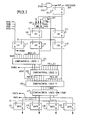
- FIG. 1 is a block diagram of the arbitration logic.
- FIG. 2 is a block diagram of the controller for the arbitration apparatus.
- FIG. 3 is a block diagram of the bump logic control.
- FIG. 4 is a table specifying the state machine controlling the arbitration logic.
- a bus master is a circuit capable of accessing and controlling at least one associated bus and which must access a bus for proper operation, e.g., direct memory transfers (DMA) for exchanging data between a system memory and an input/output device without the intervention of the system processor.
- DMA direct memory transfers
- Star arbitration is a priority request system receiving access requests in parallel, and one of several parallel requests results in an access grant to the requestor having the highest priority or according to some other criteria.
- the star arbitration system being described has four bus masters which compete in any combination and order for control of a bus.
- the limit to four bus masters makes the system description easier to understand, but the system can be expanded to any number of bus masters.
- the notation used makes the expansion of the system to more than four requestors clear and assists in the understanding of the description.
- the system described for bus access is applicable to other systems having multiple requestors for access to system resources in general.
- the star arbitration system has programmable variables which can be set by an associated processor.
- the programmable features include a priority level assignment to each bus master and a bump value associated with each bus master which controls a bus lock function.
- the system can resolve conflicts caused by the same priority level being assigned to more than one bus master.
- the bump value determines the number of request/grant cycles a higher priority bus master must relinquish to other bus masters requesting access to the bus.
- the bus masters in the following description are limited to four, denoted as A, B, C, or D and represented generally as X. Each has a separate request line, REQX, and a separate grant line, GNTX. Each bus master has an assigned priority, PX(1,0), i.e., a two-bit binary number. The value 00, or decimal 0, represents the highest priority and the value 11, decimal 3, is the lowest priority.
- PX(1,0) i.e., a two-bit binary number.
- the value 00, or decimal 0, represents the highest priority and the value 11, decimal 3, is the lowest priority.
- the priorities assigned to the bus masters need not be mutually exclusive. In other words, different bus masters can be assigned the same priority level.
- Each bus master also has an assigned bump value, BX(1,0), a two-bit binary number for purposes of illustration.
- the bump value assigned to a bus master sets the number of request/grant cycles the bus master must relinquish to other bus masters if and only if other requests are pending.
- the priority levels and bump values are supplied by the control processor over a processor bus.
- a two-phase clock is used for timing and the system is arranged so that the priority granted in response to requests is completed in one request/grant cycle by using a multilevel logic network.
- PX and BX are described as two-bit values, they can be expanded to any number of bits.
- a signal GPX is set and remains set for the number of request/grant cycles represented by the bump value, BX(1,0).
- the setting of GPX effectively causes the priority level of the associated X bus master to be bumped down by one level, e.g., from level 0 to level 1. If another bus master gets control of the bus, then the bump value is decremented at each request/grant cycle until it reaches zero, permitting the associated bus master to obtain control of the bus once again, or when the other bus masters requesting access have been bumped to the same priority level. In other words, the bump value sets the number of request/grant cycles that other bus masters can get control of the bus between successive accesses by each bus master.
- the value of BX is
- priority is granted alphabetically. That is, A precedes B, B precedes C, and so on. This is determined by the way the request lines are connected to the logic.
- Two programmable operation modes are provided.
- the mode can be set depending on whether a large number of processor memory accesses are anticipated or a large number of priority requests will be required, e.g., loading large amounts of data such as page buffers.
- REQX represents, in the preferred embodiment, the variable identifiers A, B, C, and D.
- REQX represents four signals, viz., REQA, REQB, REQC, and REQD.
- REQX can represent REQA through REQH.
- the priority and bump values can also employ more than two bits (binary digits). The notation used also makes the invention more easily understood.
- FIG. 1 shows the logic diagram for the arbitration network.
- a bus latch 101 comprising a plurality of flip-flops, is used to initiate the process by storing bits from a processor bus in response to a START signal gated by a time pulse T1 via an AND gate 103.
- the output signal from the AND gate 103 is also used as a RST signal by the control logic.
- eight bits form the bump values which are gated into an eight-bit register 109 via a multiplexor 105. That is, the stored bits from the register 101 are gated via the multiplexor 105 into the register 109 by a time pulse T2. At the same time, eight bits denoting priority assignments are gated into a register 111. At a time T1, the contents of the register 109 are gated into a register 119 and the contents of the register 111 are gated into a register 115.
- the same T1 timing pulse also stores in a four-bit register 117 active priority request signals REQA, REQB, REQC, or REQD. These signals are denoted collectively as REQX and are ORed together to generate a VREQX signal for use by the control logic.
- signals from the registers 115, 117, and 119 pass through four levels of combinatorial logic.
- the combinatorial logic at the fourth level 127 generates a new priority grant gated by a timing signal, PGNT.
- the output signals from the combinatorial logic fourth level 127 are gated into flip-flops 131, 133, 135, and 137 by a time pulse T2.
- the combinatorial logic first level 121 combines the bump value bits, BX(1,0) and the REQX bits to produce four output signals, XREQ.
- the expression forming the right-hand member of the logic equation is evaluated four times, successively substituting for X the logic variable identifiers A, B, C, and D.
- Equation (1) indicates four logical signals are generated, viz., AREQ, BREQ, CREQ, and DREQ.
- Equation (3) for LR has no X variable identifier on the left-hand side but X appears in the right-hand expression.
- the XREQ signals from the combinatorial logic first level 121 are applied as input signals to the next two levels of combinatorial logic 123 and 125.
- the XREQ signals are also ORed to supply a VXREQ signal to the controller to be used in a manner described below in more detail.
- Equation (8) is interpreted as ORing the ANDed values of XREQ with the priority bits PX(1,0) that decode to the indicated value of n.
- REQ2 (AREQ & (PA1' v PA0)') v (BREQ & (PB1' v PB0)') v (CREQ & (PC1' v PC0)') v (DREQ & (PD1' v PD0)'). (11)
- the XGNT signals are gated by a control signal PGNT, described below in more detail, to produce a GNTX signal, the final priority grant signal, which is stored in an appropriate flip-flop 131, 133, 135, or 137 by a time pulse T2.
- GNTC PGNT & CGNT & (AGNT v BGNT)' (14)
- the GNTX signals are used by the control logic and are also ORed to generate a VGNTX signal for use by the controller.
- the multiplexor 105 represents eight multiplexors in parallel, each controlled by signals XK0 and XK1. That is, there are two bit bump values for each request channel, A, B, C, and D.
- the multiplexors can reset the registers 109 by gating logical zeros when the values of XK1 and XK0 are zero.
- the XK values are one, the bits from the register 101 are gated to the register 109.
- the present bump values in register 119 are decremented and stored in register 109.
- An XK value of three recycles the previous bump values from the register 119 to the register 109.
- FIG. 3 shows a block diagram of the bump control logic.
- the control logic 301 is supplied for each value of X, four in the embodiment being described. All the input signals to the logic 301 are the same for each value of X except for the signal GNTX.
- the STATE C and DMAREQ signals are supplied by the controller logic as described below in greater detail.
- the VXREQ and the VREQX signals are described above.
- the HOLD signal is supplied by a controlling processor and can be stored in an additional latch from the processor bins in the register 101 of FIG. 1.
- the output signals, XK1 and XK0, from the bump control logic 301 control an associated multiplexor 105 shown in FIG. 1.
- the source of the signals that make up the PRI signals in equation 19 are from the controller, explained below in detail.
- LSP Load/Store Pending
- a bus master When a bus master will require control of the bus for more than one request/grant cycle, e.g., for a DMA burst of several request/grant cycles, it supplies a HOLD signal. Similarly, a HOLD signal can be supplied by a resource when it requires several contiguous request/grant cycles.
- the controller logic comprises a sequential state machine having four states.
- the signals of interest from the controller are the PGNT and the DMAREQ signals.
- the DMAREQ signal is supplied by the controller when a request has been granted to keep the controller, a state machine, from changing state or granting another request until the bus master granted access has actually assumed control of the bus.
- the DMAREQ signal is reset when a bus master assumes control of the bus.
- an output signal from the control logic sets a flip-flop 203 which supplies the DMAREQ signal.
- the flip-flop 203 is reset when a bus master is granted control of the bus as signified by the VGNTX signal.
- the input signals to the controller logic 201 include the present state signal, the signals from the processor (HOLD, LSP, ACMODE), and the VXREQ signal from the arbitration logic of FIG. 1.
- the output signals from the controller logic 201 are PGNT and the signal which sets the DMAREQ signal. Other output signals may be required by a complete system but are not of interest nor necessary for the description of the invention.
- the controller logic is completely specified by the table of FIG. 4.
- the first nine rows of FIG. 4 represent input signals and state signals of the controller.
- the bottom six rows of FIG. 4 are the output signals that result from the input and state signals.
- the top four rows are the possible machine states. (The state labels of A, B, C, and D are not related and are completely independent from the bus master labels.) In the overlap mode, the controller uses all four states. In the nonoverlap mode, only States A and C are used.
- State A is the initial state entered when the machine is first powered on and is the idle state during operation.
- State B is the waiting or hold-off state.
- State C is the GO state during which the operations of the hardware are controlled, principally by the generation of the PGNT signal.
- State D is the gap state and maintains the control signals from State C to provide a smooth transition to the idle state.
- a value of 1 indicates the machine is in the state represented by the row in which the 1 appears or that the logic signal represented by the row is true (active).
- a 0 represents the associated logic signal is false (inactive).
- a blank entry means the value of the logic signal is not required, commonly referred to as a don't-care value.
- an X indicates that the signal associated with the row in which the X appears is generated.
- the action is the logical AND result of the variables in the top nine rows of the same column.
- the first column shows the controller machine is in State A, the LSP signal is active, and the ACMODE signal is inactive.
- the action resulting from this combination of signals is to Select A, i.e., cause State A to be the next state.
- the second column represents the action taken when in State A and not in ACMODE and both the DMAREQ and HOLD signals are active while the LSP signal is inactive.
- SELECT B STATE A & LSP' & ACMODE' & DMAREQ & HOLD (25)
- State B STATE A & LSP' & ACMODE' & DMAREQ & HOLD
- State A While in State B, if the LSP signal is active while the ACMODE signal remains inactive, State A is selected.
- the last six columns show the state transitions when in the ACMODE.
- the output signals, DMAREQ and PGNT are generated only in State C when the VXREQ signal is active. Without the intermediate States B and D, however, the controller machine can respond to contiguous successive request signals.
Landscapes
- Engineering & Computer Science (AREA)
- Theoretical Computer Science (AREA)
- Physics & Mathematics (AREA)
- General Engineering & Computer Science (AREA)
- General Physics & Mathematics (AREA)
- Bus Control (AREA)
Applications Claiming Priority (2)
| Application Number | Priority Date | Filing Date | Title |
|---|---|---|---|
| US473014 | 1990-01-31 | ||
| US07/473,014 US5506989A (en) | 1990-01-31 | 1990-01-31 | Arbitration system limiting high priority successive grants |
Publications (3)
| Publication Number | Publication Date |
|---|---|
| EP0439987A2 true EP0439987A2 (fr) | 1991-08-07 |
| EP0439987A3 EP0439987A3 (en) | 1992-05-06 |
| EP0439987B1 EP0439987B1 (fr) | 1996-08-07 |
Family
ID=23877830
Family Applications (1)
| Application Number | Title | Priority Date | Filing Date |
|---|---|---|---|
| EP90480221A Expired - Lifetime EP0439987B1 (fr) | 1990-01-31 | 1990-12-28 | Système d'arbitrage limitant les autorisations successives de demandes avec haute priorité |
Country Status (4)
| Country | Link |
|---|---|
| US (1) | US5506989A (fr) |
| EP (1) | EP0439987B1 (fr) |
| JP (1) | JP2559906B2 (fr) |
| DE (1) | DE69028017T2 (fr) |
Cited By (2)
| Publication number | Priority date | Publication date | Assignee | Title |
|---|---|---|---|---|
| EP0702470A1 (fr) * | 1994-09-13 | 1996-03-20 | Telefonaktiebolaget Lm Ericsson | Procédé et dispositif pour contrÔler un réseau informatique |
| KR20030019235A (ko) * | 2001-08-31 | 2003-03-06 | 코닌클리즈케 필립스 일렉트로닉스 엔.브이. | 컬렉티브 리소스로의 기능부의 액세스를 제어하는 방법 및액세스 제어 회로 |
Families Citing this family (29)
| Publication number | Priority date | Publication date | Assignee | Title |
|---|---|---|---|---|
| US5787264A (en) * | 1995-05-08 | 1998-07-28 | Apple Computer, Inc. | Method and apparatus for arbitrating access to a shared bus |
| US6330326B1 (en) | 1998-03-27 | 2001-12-11 | At&T Corp. | Dynamic staffing of service centers to provide substantially zero-delay service |
| US6233645B1 (en) | 1998-11-02 | 2001-05-15 | Compaq Computer Corporation | Dynamically disabling speculative prefetch when high priority demand fetch opportunity use is high |
| US6530000B1 (en) | 1999-03-24 | 2003-03-04 | Qlogic Corporation | Methods and systems for arbitrating access to a disk controller buffer memory by allocating various amounts of times to different accessing units |
| US6425032B1 (en) | 1999-04-15 | 2002-07-23 | Lucent Technologies Inc. | Bus controller handling a dynamically changing mix of multiple nonpre-emptable periodic and aperiodic devices |
| US6523098B1 (en) * | 1999-12-22 | 2003-02-18 | Intel Corporation | Mechanism for efficient low priority write draining |
| US7111228B1 (en) | 2002-05-07 | 2006-09-19 | Marvell International Ltd. | System and method for performing parity checks in disk storage system |
| US7287102B1 (en) | 2003-01-31 | 2007-10-23 | Marvell International Ltd. | System and method for concatenating data |
| US7007114B1 (en) * | 2003-01-31 | 2006-02-28 | Qlogic Corporation | System and method for padding data blocks and/or removing padding from data blocks in storage controllers |
| US7492545B1 (en) | 2003-03-10 | 2009-02-17 | Marvell International Ltd. | Method and system for automatic time base adjustment for disk drive servo controllers |
| US7039771B1 (en) | 2003-03-10 | 2006-05-02 | Marvell International Ltd. | Method and system for supporting multiple external serial port devices using a serial port controller in embedded disk controllers |
| US7219182B2 (en) * | 2003-03-10 | 2007-05-15 | Marvell International Ltd. | Method and system for using an external bus controller in embedded disk controllers |
| US7064915B1 (en) | 2003-03-10 | 2006-06-20 | Marvell International Ltd. | Method and system for collecting servo field data from programmable devices in embedded disk controllers |
| US7099963B2 (en) * | 2003-03-10 | 2006-08-29 | Qlogic Corporation | Method and system for monitoring embedded disk controller components |
| US7870346B2 (en) * | 2003-03-10 | 2011-01-11 | Marvell International Ltd. | Servo controller interface module for embedded disk controllers |
| US7526691B1 (en) | 2003-10-15 | 2009-04-28 | Marvell International Ltd. | System and method for using TAP controllers |
| US7139150B2 (en) * | 2004-02-10 | 2006-11-21 | Marvell International Ltd. | Method and system for head position control in embedded disk drive controllers |
| US7120084B2 (en) | 2004-06-14 | 2006-10-10 | Marvell International Ltd. | Integrated memory controller |
| US8166217B2 (en) * | 2004-06-28 | 2012-04-24 | Marvell International Ltd. | System and method for reading and writing data using storage controllers |
| US8032674B2 (en) * | 2004-07-19 | 2011-10-04 | Marvell International Ltd. | System and method for controlling buffer memory overflow and underflow conditions in storage controllers |
| US7757009B2 (en) * | 2004-07-19 | 2010-07-13 | Marvell International Ltd. | Storage controllers with dynamic WWN storage modules and methods for managing data and connections between a host and a storage device |
| US9201599B2 (en) * | 2004-07-19 | 2015-12-01 | Marvell International Ltd. | System and method for transmitting data in storage controllers |
| US20060026329A1 (en) * | 2004-07-30 | 2006-02-02 | Yu James K | System and method for an arbiter rewind |
| US7386661B2 (en) | 2004-10-13 | 2008-06-10 | Marvell International Ltd. | Power save module for storage controllers |
| US7240267B2 (en) | 2004-11-08 | 2007-07-03 | Marvell International Ltd. | System and method for conducting BIST operations |
| US7802026B2 (en) * | 2004-11-15 | 2010-09-21 | Marvell International Ltd. | Method and system for processing frames in storage controllers |
| US7577832B2 (en) * | 2004-12-14 | 2009-08-18 | Hewlett-Packard Development Company, L.P. | Apparatus and method for booting a system |
| US7609468B2 (en) * | 2005-04-06 | 2009-10-27 | Marvell International Ltd. | Method and system for read gate timing control for storage controllers |
| US8984198B2 (en) * | 2009-07-21 | 2015-03-17 | Microchip Technology Incorporated | Data space arbiter |
Family Cites Families (5)
| Publication number | Priority date | Publication date | Assignee | Title |
|---|---|---|---|---|
| US3840859A (en) * | 1972-07-03 | 1974-10-08 | Burroughs Corp | Method and apparatus for regulating input/output traffic of a data processing system |
| US4554628A (en) * | 1981-08-17 | 1985-11-19 | Burroughs Corporation | System in which multiple devices have a circuit that bids with a fixed priority, stores all losing bids if its bid wins, and doesn't bid again until all stored bids win |
| JPH0193854A (ja) * | 1987-10-05 | 1989-04-12 | Fujitsu Ltd | バス・アービタ |
| US4920486A (en) * | 1987-11-23 | 1990-04-24 | Digital Equipment Corporation | Distributed arbitration apparatus and method for shared bus |
| JPH02181854A (ja) * | 1989-01-06 | 1990-07-16 | Toshiba Corp | 要求調停方式 |
-
1990
- 1990-01-31 US US07/473,014 patent/US5506989A/en not_active Expired - Fee Related
- 1990-12-28 EP EP90480221A patent/EP0439987B1/fr not_active Expired - Lifetime
- 1990-12-28 JP JP2408611A patent/JP2559906B2/ja not_active Expired - Lifetime
- 1990-12-28 DE DE69028017T patent/DE69028017T2/de not_active Expired - Fee Related
Cited By (5)
| Publication number | Priority date | Publication date | Assignee | Title |
|---|---|---|---|---|
| EP0702470A1 (fr) * | 1994-09-13 | 1996-03-20 | Telefonaktiebolaget Lm Ericsson | Procédé et dispositif pour contrÔler un réseau informatique |
| US5729701A (en) * | 1994-09-13 | 1998-03-17 | Telefonaktiebolaget Lm Ericsson | Method and arrangement to control a data network |
| KR20030019235A (ko) * | 2001-08-31 | 2003-03-06 | 코닌클리즈케 필립스 일렉트로닉스 엔.브이. | 컬렉티브 리소스로의 기능부의 액세스를 제어하는 방법 및액세스 제어 회로 |
| FR2829253A1 (fr) * | 2001-08-31 | 2003-03-07 | Koninkl Philips Electronics Nv | Controle d'acces dynamique d'une fonction a ressource collective |
| EP1293909A1 (fr) * | 2001-08-31 | 2003-03-19 | Koninklijke Philips Electronics N.V. | Controle d'accès dynamique d'une fonction à une ressource collective. |
Also Published As
| Publication number | Publication date |
|---|---|
| JPH04260954A (ja) | 1992-09-16 |
| DE69028017T2 (de) | 1997-02-06 |
| US5506989A (en) | 1996-04-09 |
| JP2559906B2 (ja) | 1996-12-04 |
| EP0439987A3 (en) | 1992-05-06 |
| DE69028017D1 (de) | 1996-09-12 |
| EP0439987B1 (fr) | 1996-08-07 |
Similar Documents
| Publication | Publication Date | Title |
|---|---|---|
| US5506989A (en) | Arbitration system limiting high priority successive grants | |
| EP0625753B1 (fr) | Arbitre de bus programmable de façon dynamique avec des moyens pour réaction historique | |
| US5438666A (en) | Shared memory bus system for arbitrating access control among contending memory refresh circuits, peripheral controllers, and bus masters | |
| EP1403773B1 (fr) | Dispositif de gestion de ressources | |
| KR950008227B1 (ko) | Dma 제어기를 갖는 컴퓨터 시스템 및 dma제어 방법 | |
| US6073199A (en) | History-based bus arbitration with hidden re-arbitration during wait cycles | |
| US5617575A (en) | Interprocessor priority control system for multivector processor | |
| US5388228A (en) | Computer system having dynamically programmable linear/fairness priority arbitration scheme | |
| US6584523B1 (en) | Device for organizing the access to a memory bus | |
| US5598542A (en) | Method and apparatus for bus arbitration in a multiple bus information handling system using time slot assignment values | |
| US5548762A (en) | Implementation efficient interrupt select mechanism | |
| US6505265B1 (en) | Bus arbitration system with changing arbitration rules | |
| US4730268A (en) | Distributed bus arbitration for a multiprocessor system | |
| EP0383475A2 (fr) | Arbitrage de ressources partagées | |
| US4682282A (en) | Minimum latency tie-breaking arbitration logic circuitry | |
| US5896539A (en) | Method and system for controlling access to a shared resource in a data processing system utilizing dynamically-determined weighted pseudo-random priorities | |
| EP0550147B1 (fr) | Méthode et appareil d'arbitrage basés sur la disponibilité des ressources | |
| US4181933A (en) | Memory access and sharing control system | |
| EP0071743A2 (fr) | Circuit de régénération pour une mémoire dynamique d'un processeur de données utilisant un contrôleur d'accès direct à mémoire | |
| US4896266A (en) | Bus activity sequence controller | |
| CA2051177C (fr) | Bus maitre a dispositif antiblocage sans cycles d'inactivite | |
| US5931924A (en) | Method and system for controlling access to a shared resource that each requestor is concurrently assigned at least two pseudo-random priority weights | |
| US5649209A (en) | Bus coupling information processing system for multiple access to system bus | |
| KR0144022B1 (ko) | 엘알유에 의한 중재기 | |
| US5931931A (en) | Method for bus arbitration in a multiprocessor system |
Legal Events
| Date | Code | Title | Description |
|---|---|---|---|
| PUAI | Public reference made under article 153(3) epc to a published international application that has entered the european phase |
Free format text: ORIGINAL CODE: 0009012 |
|
| AK | Designated contracting states |
Kind code of ref document: A2 Designated state(s): DE FR GB |
|
| 17P | Request for examination filed |
Effective date: 19911112 |
|
| PUAL | Search report despatched |
Free format text: ORIGINAL CODE: 0009013 |
|
| AK | Designated contracting states |
Kind code of ref document: A3 Designated state(s): DE FR GB |
|
| 17Q | First examination report despatched |
Effective date: 19941227 |
|
| GRAH | Despatch of communication of intention to grant a patent |
Free format text: ORIGINAL CODE: EPIDOS IGRA |
|
| GRAH | Despatch of communication of intention to grant a patent |
Free format text: ORIGINAL CODE: EPIDOS IGRA |
|
| GRAA | (expected) grant |
Free format text: ORIGINAL CODE: 0009210 |
|
| AK | Designated contracting states |
Kind code of ref document: B1 Designated state(s): DE FR GB |
|
| PG25 | Lapsed in a contracting state [announced via postgrant information from national office to epo] |
Ref country code: FR Effective date: 19960807 |
|
| REF | Corresponds to: |
Ref document number: 69028017 Country of ref document: DE Date of ref document: 19960912 |
|
| PG25 | Lapsed in a contracting state [announced via postgrant information from national office to epo] |
Ref country code: GB Effective date: 19961228 |
|
| EN | Fr: translation not filed | ||
| PLBE | No opposition filed within time limit |
Free format text: ORIGINAL CODE: 0009261 |
|
| STAA | Information on the status of an ep patent application or granted ep patent |
Free format text: STATUS: NO OPPOSITION FILED WITHIN TIME LIMIT |
|
| 26N | No opposition filed | ||
| GBPC | Gb: european patent ceased through non-payment of renewal fee |
Effective date: 19961228 |
|
| PG25 | Lapsed in a contracting state [announced via postgrant information from national office to epo] |
Ref country code: DE Effective date: 19970902 |