EP0441326B1 - Procédé de fabrication d'un milieu d'enregistrement optique - Google Patents
Procédé de fabrication d'un milieu d'enregistrement optique Download PDFInfo
- Publication number
- EP0441326B1 EP0441326B1 EP91101531A EP91101531A EP0441326B1 EP 0441326 B1 EP0441326 B1 EP 0441326B1 EP 91101531 A EP91101531 A EP 91101531A EP 91101531 A EP91101531 A EP 91101531A EP 0441326 B1 EP0441326 B1 EP 0441326B1
- Authority
- EP
- European Patent Office
- Prior art keywords
- group
- monomolecular film
- chemical adsorbent
- sicl
- chemical
- Prior art date
- Legal status (The legal status is an assumption and is not a legal conclusion. Google has not performed a legal analysis and makes no representation as to the accuracy of the status listed.)
- Expired - Lifetime
Links
Images


Classifications
-
- G—PHYSICS
- G11—INFORMATION STORAGE
- G11B—INFORMATION STORAGE BASED ON RELATIVE MOVEMENT BETWEEN RECORD CARRIER AND TRANSDUCER
- G11B7/00—Recording or reproducing by optical means, e.g. recording using a thermal beam of optical radiation by modifying optical properties or the physical structure, reproducing using an optical beam at lower power by sensing optical properties; Record carriers therefor
- G11B7/24—Record carriers characterised by shape, structure or physical properties, or by the selection of the material
- G11B7/26—Apparatus or processes specially adapted for the manufacture of record carriers
-
- B—PERFORMING OPERATIONS; TRANSPORTING
- B82—NANOTECHNOLOGY
- B82Y—SPECIFIC USES OR APPLICATIONS OF NANOSTRUCTURES; MEASUREMENT OR ANALYSIS OF NANOSTRUCTURES; MANUFACTURE OR TREATMENT OF NANOSTRUCTURES
- B82Y10/00—Nanotechnology for information processing, storage or transmission, e.g. quantum computing or single electron logic
-
- B—PERFORMING OPERATIONS; TRANSPORTING
- B82—NANOTECHNOLOGY
- B82Y—SPECIFIC USES OR APPLICATIONS OF NANOSTRUCTURES; MEASUREMENT OR ANALYSIS OF NANOSTRUCTURES; MANUFACTURE OR TREATMENT OF NANOSTRUCTURES
- B82Y30/00—Nanotechnology for materials or surface science, e.g. nanocomposites
-
- B—PERFORMING OPERATIONS; TRANSPORTING
- B82—NANOTECHNOLOGY
- B82Y—SPECIFIC USES OR APPLICATIONS OF NANOSTRUCTURES; MEASUREMENT OR ANALYSIS OF NANOSTRUCTURES; MANUFACTURE OR TREATMENT OF NANOSTRUCTURES
- B82Y40/00—Manufacture or treatment of nanostructures
Definitions
- the present invention relates to a process for preparing an optical recording medium.
- this invention relates to a process for preparing an optical recording medium with photochromic properties, which comprises a monomolecular film or a lamination of organic monomolecular films having polydiacetylenic bonds.
- Diacetylene derivative polymers have conductivity and nonlinear optical effects because of the presence of a ⁇ -electron conjugated system derived from polydiacetylenic bonds.
- these polymers are useful as optical- and electronic functional-materials such as optical recording media.
- optical recording media For example, as in the form of thin film such as monomolecular film.
- a thin polymer film that contains polydiacetylenic bonds is prepared by irradiating radioactive rays to a thin crystalline film of a diacetylene derivative compound.
- a single crystalline polydiacetylene thin film of large size cannot be obtained.
- the film is also prepared by irradiating radioactive rays to a monomolecular film formed by the Langmuir-Blodgett (LB) technique on a base plate, resulting in polymerization of the diacetylene groups.
- LB Langmuir-Blodgett
- the Japanese Laid-Open Publication No. 63-49757 discloses an optical recording medium including a monomolecular film or its layered films of a diacetylene derivative compound having at least a hydrophilic site and a hydrophobic site and a squarilium dye.
- the hydrophilic site of the diacetylene derivative compound is defined to be a carboxyl group, an amino group, a hydroxy group, a nitryl group, a thioalcohol group, an imino group, a sulfonic acid group, a sulfinyl group, and a metal or amine salt thereof.
- the document itself as well as further prior art documents cited therein teach to form the monomolecular film of a diacetylene derivative compound by the Langmuir-Blodgett method.
- the film prepared by this process has poor adhesiveness to the base plate.
- the film is susceptible to peeling from the base plate.
- the process will be expensive from a practical point of view because it is less efficient.
- the resulting optical recording medium has low density, and some pinholes.
- the process for preparing an optical recording medium of this invention which overcomes the above-discussed and numerous other disadvantages and deficiencies of the prior art, comprises:
- said chemical adsorbent is represented by the following formula I: wherein R1 and R2 are each independently H, an alkyl or alkoxy group having 1 to 4 carbon atoms, or halogen; l1, m1 and n1 are each independently 0 or larger integers; the sum of l1, m1 and n1 is from 5 to 25; and al is 0 or 1.
- said chemical adsorbent is any of the compounds represented by the following formulae: CH 3 -(CH 2 ) 2 -C ⁇ C-C ⁇ C-(CH 2 ) 6 -O-(CH 2 ) 3 -SiCl 3 , CH 3 -CH 2 -C ⁇ C-C ⁇ C-(CH 2 ) 6 -O-(CH 2 ) 3 -SiCl 3 , CH 3 -C ⁇ C-C ⁇ C-(CH 2 ) 17 -SiCl 3 , and H-C ⁇ C-C ⁇ C-(CH 2 ) 17 -SiCl 3
- Another feature of this invention is a process for preparing an optical recording medium comprising:
- At least one of said first and second chemical adsorbent has a substituent group on the carbon atom adjacent to said diacetylene group, and said substituent group can be conjugated with said polydiacetylenic bond, and said first and second chemical adsorbents are selected so that said first and second monomolecular films have different optical-absorption characteristics.
- At least one of said first and second chemical adsorbent is represented by the following formula II: wherein R3 and R4 are each independently H, an alkyl or alkoxyl group having 1 to 4 carbon atoms, or halogen; l2, m2 and n2 are 0 or larger integers; the sum of l2, m2 and n2 is from 5 to 25; and a2 is 0 or 1.
- Another feature of this invention is a process for preparing an optical recording medium comprising:
- At least one of said first and second chemical adsorbent has a substituent group on the carbon atom adjacent to said diacetylene group, and said substituent group can be conjugated with said polydiacetylene group, and said first and second chemical adsorbents are selected so that said first and second monomolecular films have different optical-absorption characteristics.
- said first chemical adsorbent, or first and second chemical adsorbents are represented by the following formula III: wherein R5 and R6 are each independently an alkyl group having 1 to 4 carbon atoms; R7 and R8 are each independently H, an alkyl or alkoxy group having 1 to 4 carbon atoms, or halogen; l3, m3 and n3 are 0 or larger integers; the sum of l3, m3 and n3 is from 5 to 25; and a3 is 0 or 1.
- said first and second chemical adsorbents are the compound represented by the following formula:
- a chemical adsorbent used in the process for preparing a monomolecular film provided for optical recording media of this invention having a diacetylene group (-C ⁇ C-C ⁇ C-) and -SiCl group at one molecular end.
- the chemical adsorbent is for example, represented by the following formula I: wherein R1 and R2 are each independently H, an alkyl or alkoxy group having 1 to 4 carbon atoms, or halogen; l1, m1 and n1 are each independently 0 or larger integers; the sum of l1, m1 and n1 is from 5 to 25; and a1 is 0 or 1.
- Examples of the chemical adsorbent represented by the above-described formula I are illustrated below: CH 3 -(CH 2 ) 2 -C ⁇ C-C ⁇ C-(CH 2 ) 6 -O-(CH 2 ) 3 -SiCl 3 , CH 3 -CH 2 -C ⁇ C-C ⁇ C-(CH 2 ) 6 -O-(CH 2 ) 3 -SiCl 3 , CH 3 -C ⁇ C-C ⁇ C-(CH 2 ) 17 -SiCl 3 , and H-C ⁇ C-C ⁇ C-(CH 2 ) 17 -SiCl 3
- a chemical adsorbent represented by the following formula II or III can preferably be used: wherein R3 and R4 are each independently H, an alkyl or alkoxyl group having 1 to 4 carbon atoms, or halogen; l2, m2 and n2 are each independently 0 or larger integers; the sum of l2, m2 and n2 is from 5 to 25; and a2 is 0 or 1.
- R5 and R6 are each independently an alkyl group having 1 to 4 carbon atoms
- R7 and R8 are each independently H, an alkyl or alkoxy group having 1 to 4 carbon atoms, or halogen
- l3, m3 and n3 are each independently 0 or larger integers
- the sum of l3, m3 and n3 is from 5 to 25
- a3 is 0 or 1.
- a base plate having a functional group such as hydroxyl group, amino group and carboxyl group on its surface i.e., a base plate having a hydrophilic surface
- a silicon base plate having an oxidation film formed on its surface is preferably used.
- the oxidation film is formed by the treatment of the base plate with a thermal oxidation, or formed by natural oxidation.
- the base plate is immersed in a solution of a chemical adsorbent in a non-aqueous organic solvent.
- the organic solvent which can be used includes n-hexane, carbon tetrachloride, and the like, and mixtures thereof.
- the concentration of the chemical adsorbent may be varied depending on the kinds of the base plate and its surface area, and is usually from 2.0 X 10 -3 to 5.0 X 10 -3 mol/L.
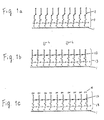
- the monomolecular film 3 formed on the base plate 1 is irradiated with ultraviolet rays to polymerize the adsorbent at the diacetylene group 2, thereby forming a polydiacetylenic bond 12 as shown in Figure 1b.
- the polydiacetylenic bond can also be formed by irradiating with X-rays, electron beams, or gamma rays instead of ultraviolet rays, all of which have higher energy than ultraviolet rays.
- a chemical adsorbent represented by the formula II or III is preferably used.
- first monomolecular film 3 is formed on the base plate 1 as described in Figure 1a by adsorbing the first chemical adsorbent of formula II.
- the first monomolecular film 3 is irradiated with ultraviolet rays to polymerize the chemical adsorbent at the diacetylene group 2 , thereby forming a polydiacetylenic bonds 12 ( Figure 1b).
- the same conversion reaction is conducted by irradiating the first monomolecular film with either X-rays, electron beams, gamma rays, etc., under oxygen atmosphere.
- the base plate having the first monomolecular film is immersed into a solution of a second chemical adsorbent having a diacetylene group, and -SiCl group at one molecular end by the same procedure as described above with respect to the first chemical adsorbent.
- the second monomolecular film is formed on the surface of the first monomolecular film.
- the second monomolecular film is also irradiated with ultraviolet rays to polymerize the chemical adsorbent at the diacetylene group, thereby forming a polydiacetylene group 22 ( Figure 1d).
- the first monomolecular film 13 after irradiation is treated with an alkaline to convert the -SiH group at the molecular end into a -SiOH group. Then, the base plate having the first monomolecular film is immersed into a solution of the second chemical adsorbent, and the second monomolecular film thus obtained is also irradiated with ultraviolet rays, thereby forming polydiacetylenic bonds.
- a chemical adsorbent represented by the formula II or III is used as the second chemical adsorbent in each process for preparing the lamination of monomolecular films described above, and then repeatingthe above-mentioned procedure consecutively, a lamination that can be used for optical recording media having three, four or more monomolecular film layers can be obtained.
- the lamination of monomolecular films can also be prepared by forming a second monomolecular film on the surface of a first monomolecular film which is not irradiated with ultraviolet rays, and then irradiating this lamination of monomolecular films with ultraviolet rays to proceed polymerization in the first and second monomolecular films, thereby forming polydiacetylenic bonds in both films.
- a chemical adsorbent having oxygen in its principal chain i.e., a compound represented by the formula I, II or III wherein al, a2 or a3 is 1
- the chemical adsorbent molecules formed on the base plate will rotate more easily. Therefore, the diacetylene group in the chemical adsorbent molecule readily reacts with the diacetylen group that is present in the neighboring molecule to form polydiacetylenic bonds.
- a monomolecular film or a lamination of monomolecular films with high polymerization degree, and with longer conjugated systems can be obtained.
- the monomolecular film or a lamination of monomolecular films having longer conjugated systems provides optical recording media of higher quality.
- the resulting first and second monomolecular films may have different optical-absorption characteristics.
- a lamination having two monomolecular films, each with different optical-absorption characteristics can be used as a multiple optical recording medium.
- a chemical adsorbent having a substituent group on the carbon atom adjacent to the diacetylene group can preferably be used. It is desirable that the substituent group be conjugated with the resulting polydiacetylenic bond.
- the substituents used for example, include benzene ring, benzene condensed rings, amino group, amide group and carboxyl group. These substituents provide a monomolecular film having longer conjugated systems, and a higher degree of polymerization.
- an optical recording medium with higher recording sensitivity can be obtained.
- the coloring matter for sensitization metallocyanine-type coloring matters, and phthalocyanine-type coloring matters can preferably be used.
- an additional optical recording medium can be prepared by using a chemical adsorbent having a group with photochromic properties, for example, spiropyran group.
- a monomolecular film with 10 to 50 ⁇ thickness is formed on a base plate, and optionally, another monomolecular film is layered thereon.
- the monomolecular film or the lamination is radiated with ion laser beams, it will turn from blue to red.
- the film or the lamination is useful for optical recording media.
- a semiconductive silicon base plate, the surface of which, has been oxidized by a thermal oxidation to form SiO 2 was provided.
- the chemical adsorbent was dissolved into a mixed solvent containing 80 wt% of n-hexane, 12 wt% of carbon tetrachloride, and 8 wt% of chloroform in a concentration of 1 X 10 -3 mol/L.
- the aforementioned silicon base plate was immersed into this solution.
- the first monomolecular film 3 was irradiated with an ultraviolet ray L having a wavelength of 200-400 nm to polymerize the chemical adsorbent, thereby forming a polymerized blue monomolecular film 13 having polydiacetylenic bonds 12 (See, Figure 1b).
- the monomolecular film was irradiated with ultraviolet rays at two different radiation doses, and then its Raman scattering spectrum was observed (Figure 2, Spectrums B and C).
- the same kind of chemical adsorbents were used to form the first and second monomolecular films, but a different kind of chemical adsorbent can also be used to form the second monomolecular film.
- the second monomolecular film was irradiated with ultraviolet rays by the same procedure as described above, resulting in a lamination of monomolecular film with a blue color.
- an additional monomolecular film can be layered on the second monomolecular film by repeating the same procedures.
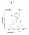
- the blue-colored lamination of monomolecular polymer films containing diacetylenic bonds as prepared above turned red when irradiated with an Ar ion laser beam, indicating that it can be used for optical recording process.
- the absorption spectrum of the irradiated lamination was identical to the absorption spectrum when the lamination was heated, and therefore it was confirmed that this reaction of color changes is due to the temperature increase of the monomolecular film caused by the radiation.
- Figure 3 shows a chart of the absorption spectrum of the lamination observed at the temperatures of 23.5°C and 60°C.
- the red optical recording medium turned blue again by cooling (i.e., the annealing effect). Therefore, in order to perform a permanent photorecording, the optical recording medium is irradiated with for example, an Ar ion laser beam so that its temperature can increase to more than 70°C, and especially 80°C. On the other hand, as long as the optical recording medium is irradiated under the condition that the temperature of the irradiated portion is 70°C or less, it can be used as a erasable type medium.
- a lamination of monomolecular films that can be used for an optical recording medium was prepared by the same procedure as in Example 1 except that a chemical adsorbent represented by the following formula was used, and that the base plate having the polymerized first monomolecular film is immersed into a NaOH solution of pH12 to convert the -SiH group at the molecular end into a -SiOH group:
Landscapes
- Engineering & Computer Science (AREA)
- Chemical & Material Sciences (AREA)
- Nanotechnology (AREA)
- Physics & Mathematics (AREA)
- Crystallography & Structural Chemistry (AREA)
- Condensed Matter Physics & Semiconductors (AREA)
- General Physics & Mathematics (AREA)
- Manufacturing & Machinery (AREA)
- Composite Materials (AREA)
- Materials Engineering (AREA)
- Mathematical Physics (AREA)
- Theoretical Computer Science (AREA)
- Optical Record Carriers And Manufacture Thereof (AREA)
- Non-Silver Salt Photosensitive Materials And Non-Silver Salt Photography (AREA)
Claims (14)
- Procédé de fabrication d'un support d'enregistrement optique comprenant les étapes suivantes :formation d'une pellicule monomoléculaire sur la surface d'une plaque de base en adsorbant un adsorbant chimique comportant un groupe diacétylène, et un groupe -SiCl à une extrémité de la molécule, etirradiation de ladite pellicule monomoléculaire avec des rayons ultraviolets pour polymériser ledit adsorbant chimique au niveau du groupe diacétylène, pour former ainsi des liaisons polydiacétyléniques.
- Procédé selon la revendication 1, dans lequel ledit adsorbant chimique est représenté par la formule I suivante:

- Procédé selon la revendication 2, dans lequel ledit adsorbant chimique est l'un des composés représentés par les formules suivantes :
CH3-(CH2)2-C≡C-C≡C-(CH2)6-O-(CH2)3-SiCl3,
CH3-CH2-C≡C-C≡C-(CH2)6-O-(CH2)3-SiCl3,
CH3-C≡C-C≡C-(CH2)17-SiCl3,
et
H-C≡C-C≡C-(CH2)17-SiCl3
- Procédé de préparation d'un support d'enregistrement optique comprenant les étapes suivantes :formation d'une première pellicule monomoléculaire sur la surface d'une plaque de base en adsorbant un premier adsorbant chimique comportant un groupe diacétylène, et un groupe -SiCl à une extrémité de la molécule,irradiation de ladite première pellicule monomoléculaire avec des rayons ultraviolets pour polymériser ledit adsorbant chimique au niveau du groupe diacétylène, pour former ainsi des liaisons polydiacétyléniques,après modification des groupes fonctionnels extérieurs de ladite première pellicule monomoléculaire polymérisée, formation d'une deuxième pellicule monomoléculaire sur la surface de ladite première pellicule monomoléculaire polymérisée en adsorbant un deuxième adsorbant chimique comportant un groupe diacétylène, et un groupe -SiCl à une extrémité de la molécule, etirradiation de ladite deuxième pellicule monomoléculaire avec des rayons ultraviolets pour polymériser ledit adsorbant chimique au niveau du groupe diacétylène, pour former ainsi des liaisons polydiacétyléniques,dans lequel au moins un desdits premier et deuxième adsorbants chimiques comporte un groupe substituant sur l'atome de carbone adjacent audit groupe diacétylène, et ledit groupe substituant peut être conjugué avec ladite liaison polydiacétylénique, et lesdits premier et deuxième adsorbants chimiques sont choisis de façon à ce que lesdites première et deuxième pellicules monomoléculaires aient des caractéristiques d'absorption optique différentes.
- Procédé selon la revendication 4, dans lequel au moins le dernier adsorbant chimique est représenté par la formule I suivante :

- Procédé selon la revendication 5, dans lequel au moins un desdits premier et deuxième adsorbants chimiques est l'un des composés représentés par les formules suivantes :
CH3-(CH2)2-C≡C-C≡C-(CH2)6-O-(CH2)3-SiCl3,
CH3-CH2-C≡C-C≡C-(CH2)6-O-(CH2)3-SiCl3,
CH3-C≡C-C≡C-(CH2)17-SiCl3,
et
H-C≡C-C≡C-(CH2)17-SiCl3
- Procédé de préparation d'un support d'enregistrement optique comprenant les étapes suivantes :formation d'une première pellicule monomoléculaire sur la surface d'une plaque de base en adsorbant un premier adsorbant chimique comportant un groupe diacétylène, un groupe -SiCl à une extrémité de la molécule, et un groupe -CH=CH2 à l'autre extrémité de la molécule,irradiation de ladite première pellicule monomoléculaire avec des rayons ultraviolets pour polymériser ledit adsorbant chimique au niveau du groupe diacétylène, pour former ainsi des liaisons polydiacétyléniques,conversion dudit groupe -CH=CH2 en un groupe -CH2-CH2OH,formation d'une deuxième pellicule monomoléculaire sur la surface de ladite première pellicule monomoléculaire polymérisée en adsorbant un deuxième adsorbant chimique comportant un groupe diacétylène, et un groupe -SiCl à une extrémité de la molécule, etirradiation de ladite deuxième pellicule monomoléculaire avec des rayons ultraviolets pour polymériser ledit adsorbant chimique au niveau du groupe diacétylène, pour former ainsi des liaisons polydiacétyléniques.
- Procédé selon la revendication 7, dans lequel au moins un desdits premier et deuxième adsorbants chimiques comporte un groupe substituant sur l'atome de carbone adjacent audit groupe diacétylène, et ledit groupe substituant peut être conjugué avec ladite liaison polydiacétylénique, et lesdits premier et deuxième adsorbants chimiques sont choisis de façon à ce que lesdites première et deuxième pellicules monomoléculaires aient des caractéristiques d'absorption optique différentes.
- Procédé selon la revendication 7, dans lequel au moins un desdits premier et deuxième adsorbants chimiques est représenté par la formule II suivante :

- Procédé selon la revendication 9, dans lequel au moins un desdits premier et deuxième adsorbants chimiques est le composé représenté par la formule suivante :
CH2=CH-(CH2)6-C≡C-C≡C-(CH2)4-O-(CH2)3-SiCl3
- Procédé de préparation d'un support d'enregistrement optique comprenant les étapes suivantes :formation d'une première pellicule monomoléculaire sur la surface d'une plaque de base en adsorbant un premier adsorbant chimique comportant un groupe diacétylène, un groupe -SiCl à une extrémité de la molécule, et un groupe -SiH à l'autre extrémité de la molécule,irradiation de ladite première pellicule monomoléculaire avec des rayons ultraviolets pour polymériser ledit adsorbant chimique au niveau du groupe diacétylène, pour former ainsi des liaisons polydiacétyléniques,conversion dudit groupe -SiH en un groupe -SiOH,formation d'une deuxième pellicule monomoléculaire sur la surface de ladite première pellicule monomoléculaire polymérisée en adsorbant un deuxième adsorbant chimique comportant un groupe diacétylène, et un groupe -SiCl à une extrémité de la molécule, etirradiation de ladite deuxième pellicule monomoléculaire avec des rayons ultraviolets pour polymériser ledit adsorbant chimique au niveau du groupe diacétylène, pour former ainsi des liaisons polydiacétyléniques.
- Procédé selon la revendication 11, dans lequel au moins un desdits premier et deuxième adsorbants chimiques comporte un groupe substituant sur l'atome de carbone adjacent audit groupe diacétylène, et ledit groupe substituant peut être conjugué avec ledit groupe polydiacétylène, et lesdits premier et deuxième adsorbants chimiques sont choisis de façon à ce que lesdites première et deuxième pellicules monomoléculaires aient des caractéristiques d'absorption optique différentes.
- Procédé selon la revendication 11, dans lequel ledit premier adsorbant chimique, ou le premier et le deuxième adsorbants chimiques sont représentés par la formule III suivante :
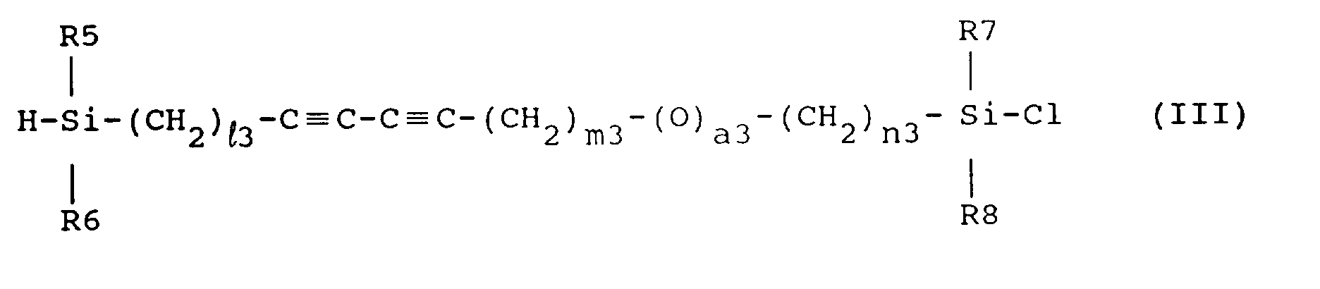
- Procédé selon la revendication 13, dans lequel lesdits premier et deuxième adsorbants chimiques sont le composé représenté par la formule suivante :

Applications Claiming Priority (2)
| Application Number | Priority Date | Filing Date | Title |
|---|---|---|---|
| JP25414/90 | 1990-02-05 | ||
| JP2025414A JPH07104571B2 (ja) | 1990-02-05 | 1990-02-05 | 光記録媒体の製造方法 |
Publications (2)
| Publication Number | Publication Date |
|---|---|
| EP0441326A1 EP0441326A1 (fr) | 1991-08-14 |
| EP0441326B1 true EP0441326B1 (fr) | 1996-12-04 |
Family
ID=12165280
Family Applications (1)
| Application Number | Title | Priority Date | Filing Date |
|---|---|---|---|
| EP91101531A Expired - Lifetime EP0441326B1 (fr) | 1990-02-05 | 1991-02-05 | Procédé de fabrication d'un milieu d'enregistrement optique |
Country Status (4)
| Country | Link |
|---|---|
| US (1) | US5130162A (fr) |
| EP (1) | EP0441326B1 (fr) |
| JP (1) | JPH07104571B2 (fr) |
| DE (1) | DE69123371T2 (fr) |
Families Citing this family (8)
| Publication number | Priority date | Publication date | Assignee | Title |
|---|---|---|---|---|
| US5273788A (en) * | 1992-07-20 | 1993-12-28 | The University Of Utah | Preparation of diamond and diamond-like thin films |
| US5661092A (en) * | 1995-09-01 | 1997-08-26 | The University Of Connecticut | Ultra thin silicon oxide and metal oxide films and a method for the preparation thereof |
| CN1246143C (zh) * | 1998-09-16 | 2006-03-22 | 松下电器产业株式会社 | 功能性膜及其制造方法、以及采用其的液晶显示元件及其制造方法 |
| US7070839B2 (en) | 1998-09-16 | 2006-07-04 | Matsushita Electric Industrial Co., Ltd. | Functional film, method of fabricating the same, liquid crystal display device using functional film, and method of fabricating the same |
| TW555790B (en) * | 2000-12-26 | 2003-10-01 | Matsushita Electric Industrial Co Ltd | Conductive organic thin film, process for producing the same, and organic photoelectronic device, electric wire, and electrode aech employing the same |
| DE60216257T2 (de) * | 2001-04-17 | 2007-06-14 | Matsushita Electric Industrial Co., Ltd., Kadoma | Leitfähiger organischer Dünnfilm, Verfahren zu dessen Herstellung, sowie Elektrde und elektrisches Kabel, die davon Gebrauch machen |
| JP7313402B2 (ja) * | 2021-06-29 | 2023-07-24 | 株式会社Kokusai Electric | 半導体装置の製造方法、基板処理装置、プログラム及びエッチング方法 |
| JP2023081626A (ja) * | 2021-12-01 | 2023-06-13 | 株式会社東芝 | ヘッドサスペンションアッセンブリ、及び磁気記録再生装置 |
Family Cites Families (5)
| Publication number | Priority date | Publication date | Assignee | Title |
|---|---|---|---|---|
| US4678736A (en) * | 1985-03-05 | 1987-07-07 | Mitsubishi Petrochemical Co., Ltd. | Optical recording media on which information is stored and method of making same |
| JPS6349757A (ja) * | 1986-08-20 | 1988-03-02 | Canon Inc | 光記録方法 |
| JPS6352135A (ja) * | 1986-08-22 | 1988-03-05 | Canon Inc | 光記録方法 |
| US4992300A (en) * | 1988-05-24 | 1991-02-12 | Matsushita Electric Industrial Co., Ltd. | Manufacturing method for a recording medium or a recording head |
| JP2506973B2 (ja) * | 1988-08-05 | 1996-06-12 | 松下電器産業株式会社 | 光記録媒体の製造方法 |
-
1990
- 1990-02-05 JP JP2025414A patent/JPH07104571B2/ja not_active Expired - Fee Related
-
1991
- 1991-02-05 EP EP91101531A patent/EP0441326B1/fr not_active Expired - Lifetime
- 1991-02-05 US US07/650,508 patent/US5130162A/en not_active Expired - Lifetime
- 1991-02-05 DE DE69123371T patent/DE69123371T2/de not_active Expired - Fee Related
Also Published As
| Publication number | Publication date |
|---|---|
| JPH03230156A (ja) | 1991-10-14 |
| EP0441326A1 (fr) | 1991-08-14 |
| DE69123371D1 (de) | 1997-01-16 |
| US5130162A (en) | 1992-07-14 |
| JPH07104571B2 (ja) | 1995-11-13 |
| DE69123371T2 (de) | 1997-03-27 |
Similar Documents
| Publication | Publication Date | Title |
|---|---|---|
| DE69332460T2 (de) | Gebrauchsverfahren von strahlungsempfindlichen Materialien | |
| Endo et al. | Interpretation of the near-infrared absorption of magnesium phthalocyanine complexes in terms of exciton coupling effects | |
| US4579837A (en) | Solid phase photosensitizer for generation of singlet oxygen | |
| EP0441326B1 (fr) | Procédé de fabrication d'un milieu d'enregistrement optique | |
| US5008127A (en) | Process for the production of a highly-orientated ultralong conjugated polymer | |
| US7892702B2 (en) | Sensitizer dyes for photoacid generating systems | |
| EP0584891A2 (fr) | Procédé pour la fabrication de films composés de couches monomoléculaires à partir de silane ayant une liaison acetylénique | |
| JP2506973B2 (ja) | 光記録媒体の製造方法 | |
| US5380889A (en) | Method of forming resist pattern and organic silane compound for forming anti-relflection film for use in such method | |
| CA2398371C (fr) | Polymere lamellaire organique/inorganique du type perovskite | |
| JP2004078224A (ja) | 光学記録材料 | |
| Sato et al. | Facile Synthesis of Bis‐pentafluoroarylated Anthracene Derivatives for N‐type Organic‐Field‐Effect Transistor Applications | |
| EP0445534A1 (fr) | Procédé pour la préparation d'un film monomoléculaire organique | |
| US20030072250A1 (en) | Optical recording material | |
| Irie et al. | Radical ions of poly (silastyrene) | |
| Gao et al. | High efficiency photoresist-free lithography of UO3 patterns from amorphous films of uranyl complexes | |
| JP2796538B2 (ja) | メロシアニン−ピロール結合体 | |
| JPH07225473A (ja) | デバイスの製造方法 | |
| JP2787339B2 (ja) | 共役系重合体およびその製法 | |
| Arabei | Photodestruction of zinc complexes of tetrabenzoporphyrins in a polymeric matrix and photosensitive materials based on them | |
| JPS62233288A (ja) | 光学的情報記録媒体 | |
| JPH06130879A (ja) | ホロク゛ラム記録材料及びそれを用いた体積位相型ホログラムの製造方法 | |
| JPS61148441A (ja) | 電荷移動錯体の形成方法 | |
| Popov et al. | Experimental study of sensitized photooxidation reaction of compounds with anthracene structure in poly (methyl methacrylate) | |
| Luna-Moreno | Study on the feasibility of a dry color printing process |
Legal Events
| Date | Code | Title | Description |
|---|---|---|---|
| PUAI | Public reference made under article 153(3) epc to a published international application that has entered the european phase |
Free format text: ORIGINAL CODE: 0009012 |
|
| AK | Designated contracting states |
Kind code of ref document: A1 Designated state(s): DE FR GB |
|
| RAP1 | Party data changed (applicant data changed or rights of an application transferred) |
Owner name: MATSUSHITA ELECTRIC INDUSTRIAL CO., LTD. |
|
| 17P | Request for examination filed |
Effective date: 19910910 |
|
| 17Q | First examination report despatched |
Effective date: 19950113 |
|
| GRAG | Despatch of communication of intention to grant |
Free format text: ORIGINAL CODE: EPIDOS AGRA |
|
| GRAH | Despatch of communication of intention to grant a patent |
Free format text: ORIGINAL CODE: EPIDOS IGRA |
|
| GRAH | Despatch of communication of intention to grant a patent |
Free format text: ORIGINAL CODE: EPIDOS IGRA |
|
| GRAA | (expected) grant |
Free format text: ORIGINAL CODE: 0009210 |
|
| AK | Designated contracting states |
Kind code of ref document: B1 Designated state(s): DE FR GB |
|
| ET | Fr: translation filed | ||
| REF | Corresponds to: |
Ref document number: 69123371 Country of ref document: DE Date of ref document: 19970116 |
|
| PLBE | No opposition filed within time limit |
Free format text: ORIGINAL CODE: 0009261 |
|
| STAA | Information on the status of an ep patent application or granted ep patent |
Free format text: STATUS: NO OPPOSITION FILED WITHIN TIME LIMIT |
|
| 26N | No opposition filed | ||
| REG | Reference to a national code |
Ref country code: GB Ref legal event code: IF02 |
|
| PGFP | Annual fee paid to national office [announced via postgrant information from national office to epo] |
Ref country code: GB Payment date: 20060201 Year of fee payment: 16 |
|
| PGFP | Annual fee paid to national office [announced via postgrant information from national office to epo] |
Ref country code: DE Payment date: 20060202 Year of fee payment: 16 |
|
| PGFP | Annual fee paid to national office [announced via postgrant information from national office to epo] |
Ref country code: FR Payment date: 20060220 Year of fee payment: 16 |
|
| GBPC | Gb: european patent ceased through non-payment of renewal fee |
Effective date: 20070205 |
|
| REG | Reference to a national code |
Ref country code: FR Ref legal event code: ST Effective date: 20071030 |
|
| PG25 | Lapsed in a contracting state [announced via postgrant information from national office to epo] |
Ref country code: DE Free format text: LAPSE BECAUSE OF NON-PAYMENT OF DUE FEES Effective date: 20070901 |
|
| PG25 | Lapsed in a contracting state [announced via postgrant information from national office to epo] |
Ref country code: FR Free format text: LAPSE BECAUSE OF NON-PAYMENT OF DUE FEES Effective date: 20070228 Ref country code: GB Free format text: LAPSE BECAUSE OF NON-PAYMENT OF DUE FEES Effective date: 20070205 |