EP0441378A2 - Frequency and/or phase characteristic control circuit - Google Patents
Frequency and/or phase characteristic control circuit Download PDFInfo
- Publication number
- EP0441378A2 EP0441378A2 EP91101695A EP91101695A EP0441378A2 EP 0441378 A2 EP0441378 A2 EP 0441378A2 EP 91101695 A EP91101695 A EP 91101695A EP 91101695 A EP91101695 A EP 91101695A EP 0441378 A2 EP0441378 A2 EP 0441378A2
- Authority
- EP
- European Patent Office
- Prior art keywords
- current
- frequency
- operational amplifier
- phase
- output
- Prior art date
- Legal status (The legal status is an assumption and is not a legal conclusion. Google has not performed a legal analysis and makes no representation as to the accuracy of the status listed.)
- Granted
Links
Images


Classifications
-
- H—ELECTRICITY
- H03—ELECTRONIC CIRCUITRY
- H03H—IMPEDANCE NETWORKS, e.g. RESONANT CIRCUITS; RESONATORS
- H03H11/00—Networks using active elements
- H03H11/46—One-port networks
- H03H11/48—One-port networks simulating reactances
-
- G—PHYSICS
- G11—INFORMATION STORAGE
- G11B—INFORMATION STORAGE BASED ON RELATIVE MOVEMENT BETWEEN RECORD CARRIER AND TRANSDUCER
- G11B20/00—Signal processing not specific to the method of recording or reproducing; Circuits therefor
- G11B20/02—Analogue recording or reproducing
- G11B20/06—Angle-modulation recording or reproducing
-
- G—PHYSICS
- G11—INFORMATION STORAGE
- G11B—INFORMATION STORAGE BASED ON RELATIVE MOVEMENT BETWEEN RECORD CARRIER AND TRANSDUCER
- G11B7/00—Recording or reproducing by optical means, e.g. recording using a thermal beam of optical radiation by modifying optical properties or the physical structure, reproducing using an optical beam at lower power by sensing optical properties; Record carriers therefor
- G11B7/08—Disposition or mounting of heads or light sources relatively to record carriers
- G11B7/09—Disposition or mounting of heads or light sources relatively to record carriers with provision for moving the light beam or focus plane for the purpose of maintaining alignment of the light beam relative to the record carrier during transducing operation, e.g. to compensate for surface irregularities of the latter or for track following
- G11B7/0941—Methods and circuits for servo gain or phase compensation during operation
Definitions
- the present invention generally relates to a frequency and/or phase characteristic control circuit. More particularly, the invention relates to a frequency and/or phase characteristic control circuit conducive to being formed in an IC (integrated circuit) for the phase compensation of servo circuits in applications such as optical disc recording and reproducing apparatus.
- IC integrated circuit
- FIG. 1 of the present application is a reproduction of such circuit and illustrates a circuit diagram of a typical frequency and/or phase characteristic control circuit wherein a signal is fed from a photo detector 1 to a focus error amplifier 3 via current/voltage converters 2. The signal is then applied to an in-phase input terminal of an operational amplifier 4. From there, the signal is sent to a voltage/current converter 5 which in turn drives a focus coil 6.
- Branch 4a comprises serially coupled reactor R1 and capacitor C1.
- Branch 4b comprises serially coupled resistor R2 and capacitor C2.
- Inverters IV3 and IV1 and IV2 are operatively disposed between the control terminal CT and the branches 4a and 4b, respectively, to provide for such selection.
- phase compensation circuit is its inability to be readily formed in an IC. This is because the time constant capacitor C1 or C2 needs to have a capacity of about 0.1 ⁇ F when the responsive frequency is to be switched between 1KHz (e.g., for a compact disc player) and 2 KHz (e.g., for a laser disc player).
- the present invention overcomes the above-described drawbacks and disadvantages and provides a frequency and/or phase characteristic control circuit wherein the frequency characteristic is stabilized against temperature fluctuations.
- the present invention provides a frequency and/or phase characteristic control circuit wherein the capacitance of a capacitor interposed between the output terminal of a current multiplier and the out-of-phase input terminal of an operational amplifier is equivalent to a multiplying ratio M of the current multiplier, thereby making the capacitance of the actual capacitor small enough so that the frequency and/or phase characteristic control circuit can readily be implemented in an IC.
- the present invention provides a frequency and/or phase characteristic control circuit in an IC where the resistance value of the load resistor for the current multiplier is made variable, thereby minimizing temperature-induced changes in frequency or phase characteristic.
- a frequency and/or phase characteristic control circuit comprising: (1) a current multiplier having a multiplying ratio and containing an input terminal to be supplied with an input voltage, a voltage/current converter supplied with the input voltage so as to produce a pair of current signals at an output thereof, a pair of diode junctions supplied with the pair of current signals, a differential amplifier having first and second transistors and a current source, the first and second transistors being supplied with the voltage across the pair of diode junctions to produce a multiplied output current, and an output terminal connected to the output of the differential amplifier so as to produce output voltage across a load resistor proportional to the multiplied output current; (b) an operational amplifier having an in-phase input terminal, an out-of-phase input terminal and an output terminal; (c) a capacitor connected between the output terminal of the current multiplier and the out-of-phase input terminal of the operational amplifier; (d) a first impedance connected between the input terminal of the current multiplier and the out-of-
- FIG. 1 is a circuit diagram of a typical prior art frequency and/or phase characteristic control circuit.
- FIG. 2 is a circuit diagram of a frequency and/or phase characteristic control circuit embodying the present invention.
- FIG. 3 is a variation of the circuit diagram of the embodiment of FIG. 2.
- FIG. 4 is another equivalent circuit diagram of the circuit diagram of the embodiment of FIG. 2.
- FIGS. 5A and 5B are a gain characteristic chart and a phase characteristic chart, respectively, for use in describing the invention.
- FIG. 2 is a circuit diagram of a first frequency and/or phase characteristic control circuit embodying the invention.
- reference numeral 8 identifies a current multiplier
- numeral 9 identifies an operational amplifier.
- the current multiplier 8 comprises: a differential amplifier 10 having a pair of transistors Q1 and Q2 and a constant current supply transistor Q3; a pair of transistors Q4 and Q5 interposed as a pair of diode junctions between each base of the pair of transistors Q1 and Q2 on the one hand and a reference voltage supply V r on the other hand, the bases of the transistors Q4 and Q5 being interconnected; and a V/I converter 12 for converting an input voltage V i supplied to an input terminal 11 into an input current I1.
- the V/I converter 12 comprises transistors Q6 and Q7.
- the transistor Q6 has its base and collector connected respectively to the input terminal 11 and to the emitter of the transistor Q4.
- the transistor Q7 has its base and collector connected respectively to a bias voltage supply V b and to the emitter of the transistor Q5.
- the emitters of the transistors Q6 and Q7 are interconnected through a resistor 13 having a resistance value of R1. These emitters are also connected to the collectors of the transistors Q8 and Q9 whose emitters are connected to a reference potential point (i.e., ground).
- Two equivalent bias currents I1 flowing through the transistors Q8 and Q9 are supplied to the emitters of the transistors Q4 and Q5 via the collector emitter circuit of the transistor Q6 and Q7.
- the base and emitter of the constant current supply transistor Q3 are connected in parallel with the base and emitter of a diode connected transistor Q10 to constitute a current mirror circuit.
- the base and emitter of the transistors Q8 and Q9 are connected in parallel with the base and emitter of a diode connected transistor Q11 thereby to constitute a current mirror circuit.
- the collector of the transistor Q11 is connected to a voltage supply V CC via a resistor 14 having a resistance value of R2.
- the collector of the transistor Q10 is also connected to the voltage supply V CC via a resistor 15 having a resistance value of R3.
- a current 2I2 flowing through the constant current supply transistor Q3 of the differential amplifier 10 branches out to the transistors Q1 and Q2.
- a common connection point of the collectors of the transistors Q13 and Q2 is connected to an output terminal 16.
- This output current i2 is obtained by multiplying the input current i1 by the ratio of half of the current 2I2 flowing between the collector and emitter of the constant current supply transistor Q3 to the bias current I1 flowing between the collector and emitter of the transistors Q4 and Q5. From the above current flow, a current 212 is obtained by a push-pull connection.
- the output current 2I2 generates an output voltage V0 at a load resistor which has a resistance value of R L and is connected to the output terminal 16, the output voltage V0 being proportional to the output current i2.
- a capacitor 18 having a capacitance of C is connected between the output terminal 16 of the current multiplier 8 and the out-of-phase input terminal (negative) of the operational amplifier 9.
- a first impedance element 19 having an impedance value of Z1 is connected between the input terminal 11 of the current multiplier 8 and the out-of-phase input terminal (negative) of the operational amplifier 9.
- a second impedance element 20 having an impedance value of Z2 is connected between the out-of-phase input terminal (negative) and output terminal 21 of the operational amplifier 9.
- the two transistors Q1 and Q2 in the differential amplifier 10 have the same characteristic as the transistors Q4 and Q5 whose base and emitter circuit constitute a pair of diode junctions, the sum of a voltage V BE4 between the base and emitter of the transistor Q4 and a voltage V BE1 between the base and emitter of the transistor Q1 becomes equal to the sum of a voltage V BE5 between the base and emitter of the transistor Q5 and a voltage V BE2 between the base and emitter of the transistor Q2.
- each emitter-to-base voltage can be expressed as follows: where, q stands for the electric charge of an electron, K for Boltzmann's constant, T for the absolute temperature, and i s for the reverse saturation current. It is assumed that the current i s of each transistor is the same.
- a transfer function G (s) across the input terminal 11 to the output terminal 21 is obtained using the equation Therefore, the frequency characteristic is controlled by varying the multiplying ratio M of the current multiplier 8.
- MCZ1 indicates that the time constant apparently is given as if multiplied by M. This reduces the required capacitance of the capacitor 18, which makes it easier to form the circuit in an IC.
- the resistance ratio inside the IC becomes: This keeps the frequency characteristic stabilized against temperature fluctuations.
- the multiplying ratio M of the current multiplier 8 is set to 5.5.
- the first impedance element 19 comprises attentuation resistors 19a (130 K ⁇ ) and 19b (37 K ⁇ ) and a feedback resistor 19c (330 K ⁇ ).
- the second impedance element 20 comprises attenuation resistors 20a (110 K ⁇ ) and 20b (7.5 k ⁇ ), a feedback resistor 20c (463 K ⁇ ) and a capacitor (1 pF) for preventing oscillation.
- the capacitor 18 has a capacitance (c) of 68 pF, and the load resistor 17 has a resistance (R L ) of 165 K ⁇ .
- the peak frequency f0 of the phase characteristic is obtained using the following equation: as depicted in FIG. 5 (B) in which a peak ⁇ is observed at around 2 KHz.
- the resistance value R L of the load resistor 17 is multiplied by 1/n so as to turn f1 into nf1, f2 into nf2, and f0 into
- the load resistor 17 preferably comprises an electronic switch that controls a plurality of resistors using a control signal external to the IC. That is, the resistance value R L may alternatively be varied by operating the electronic switch.
- the frequency and/or phase characteristic control circuit is a circuit wherein the capacitance of the capacitor interposed between the output terminal of the current multiplier and the out-of-phase input terminal of the operational amplifier is multiplied by the multiplying ratio M of the current multiplier. This means that the actual capacitance of the capacitor is small enough to permit the circuit to be readily formed in an IC.
Landscapes
- Engineering & Computer Science (AREA)
- Signal Processing (AREA)
- Networks Using Active Elements (AREA)
- Formation And Processing Of Food Products (AREA)
- Semiconductor Lasers (AREA)
Abstract
Description
- The present invention generally relates to a frequency and/or phase characteristic control circuit. More particularly, the invention relates to a frequency and/or phase characteristic control circuit conducive to being formed in an IC (integrated circuit) for the phase compensation of servo circuits in applications such as optical disc recording and reproducing apparatus.
- In Japanese Laid-open Utility Model No. 63-6516 there is disclosed a phase compensation circuit that includes a switching circuit for selecting a time constant. FIG. 1 of the present application is a reproduction of such circuit and illustrates a circuit diagram of a typical frequency and/or phase characteristic control circuit wherein a signal is fed from a
photo detector 1 to afocus error amplifier 3 via current/voltage converters 2. The signal is then applied to an in-phase input terminal of anoperational amplifier 4. From there, the signal is sent to a voltage/current converter 5 which in turn drives afocus coil 6. - As illustrated, coupled to another input of the
operative amplifier 4 are two selectable time constant establishingbranches Branch 4a comprises serially coupled reactor R₁ and capacitor C₁.Branch 4b comprises serially coupled resistor R₂ and capacitor C₂. These time constant branches are selected in accordance with the application of a control signal at a control terminal CT. Inverters IV₃ and IV₁ and IV₂ are operatively disposed between the control terminal CT and thebranches - One disadvantage of this prior art phase compensation circuit is its inability to be readily formed in an IC. This is because the time constant capacitor C₁ or C₂ needs to have a capacity of about 0.1 µF when the responsive frequency is to be switched between 1KHz (e.g., for a compact disc player) and 2 KHz (e.g., for a laser disc player).
- The present invention overcomes the above-described drawbacks and disadvantages and provides a frequency and/or phase characteristic control circuit wherein the frequency characteristic is stabilized against temperature fluctuations.
- Further, the present invention provides a frequency and/or phase characteristic control circuit wherein the capacitance of a capacitor interposed between the output terminal of a current multiplier and the out-of-phase input terminal of an operational amplifier is equivalent to a multiplying ratio M of the current multiplier, thereby making the capacitance of the actual capacitor small enough so that the frequency and/or phase characteristic control circuit can readily be implemented in an IC.
- Yet further, the present invention provides a frequency and/or phase characteristic control circuit in an IC where the resistance value of the load resistor for the current multiplier is made variable, thereby minimizing temperature-induced changes in frequency or phase characteristic.
- To these ends, the present invention provides in one embodiment a frequency and/or phase characteristic control circuit comprising: (1) a current multiplier having a multiplying ratio and containing an input terminal to be supplied with an input voltage, a voltage/current converter supplied with the input voltage so as to produce a pair of current signals at an output thereof, a pair of diode junctions supplied with the pair of current signals, a differential amplifier having first and second transistors and a current source, the first and second transistors being supplied with the voltage across the pair of diode junctions to produce a multiplied output current, and an output terminal connected to the output of the differential amplifier so as to produce output voltage across a load resistor proportional to the multiplied output current; (b) an operational amplifier having an in-phase input terminal, an out-of-phase input terminal and an output terminal; (c) a capacitor connected between the output terminal of the current multiplier and the out-of-phase input terminal of the operational amplifier; (d) a first impedance connected between the input terminal of the current multiplier and the out-of-phase input terminal of the operational amplifier; (e) a second impedance connected between the out-of-phase input terminal and the output terminal of the operational amplifier; wherein the frequency and/or phase of the output signal of the operational amplifier is controlled by varying the multiplying ratio of the current multiplier.
- These and other features of the invention will become more apparent with reference to the following detailed description of the presently preferred embodiment and accompanying drawings.
- FIG. 1 is a circuit diagram of a typical prior art frequency and/or phase characteristic control circuit.
- FIG. 2 is a circuit diagram of a frequency and/or phase characteristic control circuit embodying the present invention.
- FIG. 3 is a variation of the circuit diagram of the embodiment of FIG. 2.
- FIG. 4 is another equivalent circuit diagram of the circuit diagram of the embodiment of FIG. 2.
- FIGS. 5A and 5B are a gain characteristic chart and a phase characteristic chart, respectively, for use in describing the invention.
- Preferred embodiments of the present invention will now be described with reference to FIGS. 2-6.
- FIG. 2 is a circuit diagram of a first frequency and/or phase characteristic control circuit embodying the invention. In FIG. 2,
reference numeral 8 identifies a current multiplier, andnumeral 9 identifies an operational amplifier. Thecurrent multiplier 8 comprises: adifferential amplifier 10 having a pair of transistors Q₁ and Q₂ and a constant current supply transistor Q₃; a pair of transistors Q₄ and Q₅ interposed as a pair of diode junctions between each base of the pair of transistors Q₁ and Q₂ on the one hand and a reference voltage supply Vr on the other hand, the bases of the transistors Q₄ and Q₅ being interconnected; and a V/I converter 12 for converting an input voltage Vi supplied to aninput terminal 11 into an input current I₁. The V/I converter 12 comprises transistors Q₆ and Q₇. The transistor Q₆ has its base and collector connected respectively to theinput terminal 11 and to the emitter of the transistor Q₄. The transistor Q₇ has its base and collector connected respectively to a bias voltage supply Vb and to the emitter of the transistor Q₅. The emitters of the transistors Q₆ and Q₇ are interconnected through aresistor 13 having a resistance value of R₁. These emitters are also connected to the collectors of the transistors Q₈ and Q₉ whose emitters are connected to a reference potential point (i.e., ground). Two equivalent bias currents I₁ flowing through the transistors Q₈ and Q₉ are supplied to the emitters of the transistors Q₄ and Q₅ via the collector emitter circuit of the transistor Q₆ and Q₇. - The base and emitter of the constant current supply transistor Q₃ are connected in parallel with the base and emitter of a diode connected transistor Q₁₀ to constitute a current mirror circuit. The base and emitter of the transistors Q₈ and Q₉ are connected in parallel with the base and emitter of a diode connected transistor Q₁₁ thereby to constitute a current mirror circuit. The collector of the transistor Q₁₁ is connected to a voltage supply VCC via a
resistor 14 having a resistance value of R₂. The collector of the transistor Q₁₀ is also connected to the voltage supply VCC via aresistor 15 having a resistance value of R₃. A current 2I₂ flowing through the constant current supply transistor Q₃ of thedifferential amplifier 10 branches out to the transistors Q₁ and Q₂. This causes a current I₂ to be supplied to transistors Q₁₂ and Q₁₃ which are connected to the collectors of the transistors Q₁ and Q₂ to another current mirror circuit. A common connection point of the collectors of the transistors Q₁₃ and Q₂ is connected to anoutput terminal 16. - The collectors of the transistors Q₁ and Q₂ in the
differential amplifier 10 are supplied with an output current i₂ (wherein, i₂ = i₁ . I₂/I₁). This output current i₂ is obtained by multiplying the input current i₁ by the ratio of half of the current 2I₂ flowing between the collector and emitter of the constant current supply transistor Q₃ to the bias current I₁ flowing between the collector and emitter of the transistors Q₄ and Q₅. From the above current flow, a current 2₁₂ is obtained by a push-pull connection. The output current 2I₂ generates an output voltage V₀ at a load resistor which has a resistance value of RL and is connected to theoutput terminal 16, the output voltage V₀ being proportional to the output current i₂. - A
capacitor 18 having a capacitance of C is connected between theoutput terminal 16 of thecurrent multiplier 8 and the out-of-phase input terminal (negative) of theoperational amplifier 9. Afirst impedance element 19 having an impedance value of Z₁ is connected between theinput terminal 11 of thecurrent multiplier 8 and the out-of-phase input terminal (negative) of theoperational amplifier 9. Asecond impedance element 20 having an impedance value of Z₂ is connected between the out-of-phase input terminal (negative) andoutput terminal 21 of theoperational amplifier 9. - In operation, when the two transistors Q₁ and Q₂ in the
differential amplifier 10 have the same characteristic as the transistors Q₄ and Q₅ whose base and emitter circuit constitute a pair of diode junctions, the sum of a voltage VBE4 between the base and emitter of the transistor Q₄ and a voltage VBE1 between the base and emitter of the transistor Q₁ becomes equal to the sum of a voltage VBE5 between the base and emitter of the transistor Q₅ and a voltage VBE2 between the base and emitter of the transistor Q₂. Thus, the following equation is obtained:

Meanwhile, each emitter-to-base voltage can be expressed as follows:

where, q stands for the electric charge of an electron, K for Boltzmann's constant, T for the absolute temperature, and is for the reverse saturation current. It is assumed that the current is of each transistor is the same. - By substituting equations (2) through (5) in equation (1), one obtains the following equation

- If the resistance value R₁ of the
resistor 13 is sufficiently larger than the emitter resistance (26Ω/1 mA), then
Thus, the output voltage V₀ of thecurrent multiplier 8 is given by the equation
where, a multiplying ratio of
- A transfer function G(s) across the
input terminal 11 to theoutput terminal 21 is obtained using the equation
Therefore, the frequency characteristic is controlled by varying the multiplying ratio M of thecurrent multiplier 8. - As is evident from equation (8), MCZ₁ indicates that the time constant apparently is given as if multiplied by M. This reduces the required capacitance of the
capacitor 18, which makes it easier to form the circuit in an IC. - If the
resistor 14 having the resistance value R₂ is externally installed, the resistance ratio inside the IC becomes:
This keeps the frequency characteristic stabilized against temperature fluctuations. - Referring now to FIG. 3, in one embodiment, the multiplying ratio M of the
current multiplier 8 is set to 5.5. Thefirst impedance element 19 comprisesattentuation resistors 19a (130 KΩ) and 19b (37 KΩ) and afeedback resistor 19c (330 KΩ). Thesecond impedance element 20 comprisesattenuation resistors 20a (110 KΩ) and 20b (7.5 kΩ), afeedback resistor 20c (463 KΩ) and a capacitor (1 pF) for preventing oscillation. Thecapacitor 18 has a capacitance (c) of 68 pF, and theload resistor 17 has a resistance (RL) of 165 KΩ. In this embodiment, one obtains the following relationships:


The frequency characteristic of the equivalent circuit in FIG. 3 has an inflection point at
and at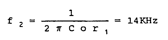
This is indicated by character G in FIG. 5 (A). - The equivalent circuit is illustrated in FIG. 4.
- The peak frequency f₀ of the phase characteristic is obtained using the following equation:

as depicted in FIG. 5 (B) in which a peak Φ is observed at around 2 KHz. - In the equation providing the multiplying factor M for the
current multiplier 8,
the resistance value RL of theload resistor 17 is multiplied by 1/n so as to turn f₁ into nf₁, f₂ into nf₂, and f₀ into
Thus, the frequency and phase characteristic is varied as desired. For example, if n = 1/2, then f₀ is set at approximately for 1 kHz. Theload resistor 17 preferably comprises an electronic switch that controls a plurality of resistors using a control signal external to the IC. That is, the resistance value RL may alternatively be varied by operating the electronic switch. - As described, the frequency and/or phase characteristic control circuit according to the invention is a circuit wherein the capacitance of the capacitor interposed between the output terminal of the current multiplier and the out-of-phase input terminal of the operational amplifier is multiplied by the multiplying ratio M of the current multiplier. This means that the actual capacitance of the capacitor is small enough to permit the circuit to be readily formed in an IC.
- Where the resistance value of the load resistor arrangement in the current multiplier is varied in a frequency and/or phase characteristic control circuit formed in an IC, temperature-induced fluctuations in the frequency or phase characteristic are significantly reduced.
- It is to be understood that while the invention has been described in conjunction with specific embodiments, it is evident that many alternatives, modifications and variations will become apparent to those skilled in the art in light of the foregoing description. Accordingly, it is intended that the present invention embrace all such alternatives, modifications and variations as fall within the spirit and scope of the appended claims.
Claims (6)
- A frequency and/or phase characteristic control circuit comprising:(a) a current multiplier (8) having a multiplying ratio and containing an input terminal (11) to be supplied with an input voltage, a voltage/current converter (12) supplied with said input voltage so as to produce a pair of current. signals at the output thereof, a pair of diode junctions (Q₄,Q₅) supplied with said pair of current signals, a differential amplifier (10) having first and second transistors (Q₁,Q₂) and a current source (Q₃), said first and second transistors (Q₁,Q₂) being supplied with the voltage across said pair of diode junctions (Q₄,Q₅) to produce a multiplied output current, and an output terminal (16) connected to the output of said differential amplifier (10) so as to produce output voltage across a load resistor (17) proportional to said multiplied output current;(b) an operational amplifier (9) having an in-phase input terminal, an out-of-phase input terminal and an output terminal;(c) a capacitor (18) connected between the output terminal of said current multiplier (8) and the out-of-phase input terminal of said operational amplifier (9);(d) a first impedance (19) connected between the input terminal (11) of said current multiplier (8) and the out-of-phase input terminal of said operational amplifier (9); and(e) a second impedance (20) connected between the out-of-phase input terminal and the output terminal of said operational amplifier (9); wherein the frequency and/or phase of the output signal of said operational amplifier (9) is controlled by varying the multiplying ratio of said current multiplier (8).
- A frequency and/or phase characteristic control circuit according to claim 1, wherein the multiplying ratio of said current multiplier is controlled by varying the resistance (RL) of said load resistor (17).
- A frequency and/or phase characteristic control circuit according to claim 1, wherein the multiplying ratio of said current multiplier is controlled by varying the current ratio of said voltage/current converter (12) and said differential amplifier (10).
- A frequency and/or phase characteristic control circuit according to anyone of claims 1 to 3, wherein said input voltage of said current multiplier (8) is a servo signal and the output signal of said operational amplifier (9) is used for driving a focus coil.
- A frequency and/or phase characteristic control circuit according to anyone of claims 1 to 4, wherein said frequency and/or phase characteristic of said operational amplifier (9) is controlled by varying the resistance (RL) of said load resistor (17) in response to a signal generated by a device such as a laser disc player or a compact disc player.
- A frequency and/or phase characteristic control circuit according to anyone of claims 1 to 5, wherein said current multiplier (8) and said operational amplifier (9) are formed in a single-chip integrated circuit.
Applications Claiming Priority (2)
| Application Number | Priority Date | Filing Date | Title |
|---|---|---|---|
| JP2028372A JPH03234110A (en) | 1990-02-09 | 1990-02-09 | Frequency characteristic variable circuit |
| JP28372/90 | 1990-02-09 |
Publications (3)
| Publication Number | Publication Date |
|---|---|
| EP0441378A2 true EP0441378A2 (en) | 1991-08-14 |
| EP0441378A3 EP0441378A3 (en) | 1992-02-26 |
| EP0441378B1 EP0441378B1 (en) | 1995-04-19 |
Family
ID=12246799
Family Applications (1)
| Application Number | Title | Priority Date | Filing Date |
|---|---|---|---|
| EP91101695A Expired - Lifetime EP0441378B1 (en) | 1990-02-09 | 1991-02-07 | Frequency and/or phase characteristic control circuit |
Country Status (6)
| Country | Link |
|---|---|
| US (2) | US5115154A (en) |
| EP (1) | EP0441378B1 (en) |
| JP (1) | JPH03234110A (en) |
| KR (1) | KR920005793A (en) |
| CA (1) | CA2035370C (en) |
| DE (1) | DE69108949T2 (en) |
Families Citing this family (17)
| Publication number | Priority date | Publication date | Assignee | Title |
|---|---|---|---|---|
| EP0490016B1 (en) * | 1990-12-12 | 1995-08-09 | STMicroelectronics S.r.l. | Integrated circuit for generating a temperature independent current proportional to the voltage difference between a signal and a reference voltage |
| US5391944A (en) * | 1992-01-22 | 1995-02-21 | Matsushita Electric Industrial Co., Ltd. | Image-tone control circuit and gradient adjusting circuit therefor |
| DE4227282C1 (en) * | 1992-08-18 | 1993-11-25 | Siemens Ag | Digital power switch |
| US5374859A (en) * | 1993-04-30 | 1994-12-20 | Intel Corporation | Low power dual power supply high resolution comparator |
| US6277314B1 (en) * | 1998-02-04 | 2001-08-21 | Flextech Packaging, Ltd. | System and method for producing polymeric film |
| US6210727B1 (en) * | 2000-02-01 | 2001-04-03 | American Extrusion International, Corp. | Method and means of controlling a food extruder as a function of bulk density of the extruded product |
| US20030056657A1 (en) * | 2001-09-27 | 2003-03-27 | Warner Richard Jarvis | Method and means for selectively cooling an extrusion die head |
| FR2843799B1 (en) * | 2002-08-21 | 2005-02-11 | Tremark Technologies Inc | BARREL DOSING MACHINE |
| WO2005013418A1 (en) | 2003-08-01 | 2005-02-10 | Sanyo Electric Co., Ltd. | Patch antenna |
| US7569241B2 (en) * | 2003-11-19 | 2009-08-04 | Conagra Foods Rdm, Inc. | Magnetic alignment system for scraped-surface heat exchanger and method |
| CN101268918B (en) * | 2007-03-23 | 2012-04-25 | 厦门灿坤实业股份有限公司 | A temperature-adjustable electric heating grill |
| US7794134B1 (en) | 2010-02-24 | 2010-09-14 | Wenger Manufacturing, Inc. | Method of preconditioner control with reduced or zero waste |
| US9510617B2 (en) | 2012-04-13 | 2016-12-06 | Frito-Lay North America, Inc. | Micropellets of fine particle nutrients and methods of incorporating same into snack food products |
| US9271523B2 (en) | 2012-05-23 | 2016-03-01 | Dennis Williams | Rotor assembly with one-piece finger member |
| US9669574B2 (en) * | 2014-11-11 | 2017-06-06 | Frito-Lay North America, Inc. | Twin screw rotary head extruder, method of extrusion and random extruded products |
| US9955712B2 (en) | 2014-11-11 | 2018-05-01 | Frito-Lay North America, Inc. | Rotary head extruder |
| US20190387784A1 (en) * | 2018-04-13 | 2019-12-26 | Zongen Li | Electromagnetically tightening & losing, electromagnetically cutting and second eatable-stuff input puffing machine |
Family Cites Families (9)
| Publication number | Priority date | Publication date | Assignee | Title |
|---|---|---|---|---|
| US2295868A (en) * | 1939-04-27 | 1942-09-15 | Flakall Corp | Process for preparing food products |
| US2350643A (en) * | 1939-04-27 | 1944-06-06 | Flakall Corp | Machine for preparing food products |
| GB1482215A (en) * | 1974-04-08 | 1977-08-10 | Brookdeal Electronics Ltd | Phase sensitive detector circuits |
| JPS58155527A (en) * | 1982-03-10 | 1983-09-16 | Hitachi Ltd | Focus pull-in circuit of optical disc player |
| JPS62208247A (en) * | 1986-03-07 | 1987-09-12 | Nippon Saitetsuku Kk | Production of gelatinized cereal |
| JPS636516A (en) * | 1986-06-27 | 1988-01-12 | Fuji Xerox Co Ltd | Optical writing device |
| AU602031B2 (en) * | 1986-12-29 | 1990-09-27 | Sony Corporation | Filter circuit |
| US4890065A (en) * | 1987-03-26 | 1989-12-26 | Howe Technologies Corporation | Relative time delay correction system utilizing window of zero correction |
| US4994286A (en) * | 1988-05-09 | 1991-02-19 | Agrichem, Inc. | Grain conditioning method |
-
1990
- 1990-02-09 JP JP2028372A patent/JPH03234110A/en active Pending
-
1991
- 1991-02-05 CA CA002035370A patent/CA2035370C/en not_active Expired - Fee Related
- 1991-02-06 US US07/651,609 patent/US5115154A/en not_active Expired - Lifetime
- 1991-02-07 DE DE69108949T patent/DE69108949T2/en not_active Expired - Fee Related
- 1991-02-07 EP EP91101695A patent/EP0441378B1/en not_active Expired - Lifetime
- 1991-02-08 KR KR1019910002127A patent/KR920005793A/en not_active Withdrawn
- 1991-03-11 US US07/667,469 patent/US5143738A/en not_active Expired - Fee Related
Also Published As
| Publication number | Publication date |
|---|---|
| CA2035370C (en) | 2001-04-10 |
| KR920005793A (en) | 1992-04-03 |
| US5143738A (en) | 1992-09-01 |
| DE69108949D1 (en) | 1995-05-24 |
| EP0441378A3 (en) | 1992-02-26 |
| CA2035370A1 (en) | 1991-08-10 |
| JPH03234110A (en) | 1991-10-18 |
| US5115154A (en) | 1992-05-19 |
| EP0441378B1 (en) | 1995-04-19 |
| DE69108949T2 (en) | 1995-08-31 |
Similar Documents
| Publication | Publication Date | Title |
|---|---|---|
| EP0441378A2 (en) | Frequency and/or phase characteristic control circuit | |
| EP0442492B1 (en) | Active filter | |
| EP0196906B1 (en) | Automatic gain control detection circuit | |
| US4340868A (en) | Current mode biquadratic active filter | |
| US4157493A (en) | Delta VBE generator circuit | |
| US4404529A (en) | Lowpass filter with electronic control of cutoff and resonance | |
| US4300102A (en) | Variable gain control circuit | |
| US4437070A (en) | Amplifier arrangement whose overall gain is controllable by means of a control voltage | |
| EP0828344A2 (en) | Integrated circuit and method for generating a transimpedance function | |
| JPH01318308A (en) | Logarithmic amplifier | |
| JP3404209B2 (en) | Transimpedance amplifier circuit | |
| JPH0537822A (en) | Gamma correction circuit | |
| US4500932A (en) | Signal processing circuit | |
| JPH04230588A (en) | Integrator of transconductor capacitor in compressing and expanding current mode | |
| JPH0648775B2 (en) | Leapfrog filter | |
| JPS5924561B2 (en) | Control amount generation circuit that controls the transmission amount of an electronically controllable amplification element or attenuation element | |
| GB2263207A (en) | Voltage controlled oscillator using negative - resistive feedback | |
| US4247789A (en) | Electronic circuitry for multiplying/dividing analog input signals | |
| EP0186401B1 (en) | Controllable effective resistance circuits | |
| JPH02193402A (en) | Optical coupling element | |
| JPH0154884B2 (en) | ||
| GB2095954A (en) | Compander system | |
| JPS631455Y2 (en) | ||
| JPS6161286B2 (en) | ||
| JPS6228884B2 (en) |
Legal Events
| Date | Code | Title | Description |
|---|---|---|---|
| PUAI | Public reference made under article 153(3) epc to a published international application that has entered the european phase |
Free format text: ORIGINAL CODE: 0009012 |
|
| AK | Designated contracting states |
Kind code of ref document: A2 Designated state(s): DE FR GB NL |
|
| PUAL | Search report despatched |
Free format text: ORIGINAL CODE: 0009013 |
|
| AK | Designated contracting states |
Kind code of ref document: A3 Designated state(s): DE FR GB NL |
|
| 17P | Request for examination filed |
Effective date: 19920826 |
|
| 17Q | First examination report despatched |
Effective date: 19940630 |
|
| GRAA | (expected) grant |
Free format text: ORIGINAL CODE: 0009210 |
|
| AK | Designated contracting states |
Kind code of ref document: B1 Designated state(s): DE FR GB NL |
|
| REF | Corresponds to: |
Ref document number: 69108949 Country of ref document: DE Date of ref document: 19950524 |
|
| ET | Fr: translation filed | ||
| PLBE | No opposition filed within time limit |
Free format text: ORIGINAL CODE: 0009261 |
|
| STAA | Information on the status of an ep patent application or granted ep patent |
Free format text: STATUS: NO OPPOSITION FILED WITHIN TIME LIMIT |
|
| 26N | No opposition filed | ||
| REG | Reference to a national code |
Ref country code: GB Ref legal event code: IF02 |
|
| PGFP | Annual fee paid to national office [announced via postgrant information from national office to epo] |
Ref country code: GB Payment date: 20020206 Year of fee payment: 12 |
|
| PGFP | Annual fee paid to national office [announced via postgrant information from national office to epo] |
Ref country code: FR Payment date: 20020212 Year of fee payment: 12 |
|
| PGFP | Annual fee paid to national office [announced via postgrant information from national office to epo] |
Ref country code: DE Payment date: 20020227 Year of fee payment: 12 |
|
| PGFP | Annual fee paid to national office [announced via postgrant information from national office to epo] |
Ref country code: NL Payment date: 20020228 Year of fee payment: 12 |
|
| PG25 | Lapsed in a contracting state [announced via postgrant information from national office to epo] |
Ref country code: GB Free format text: LAPSE BECAUSE OF NON-PAYMENT OF DUE FEES Effective date: 20030207 |
|
| PG25 | Lapsed in a contracting state [announced via postgrant information from national office to epo] |
Ref country code: NL Free format text: LAPSE BECAUSE OF NON-PAYMENT OF DUE FEES Effective date: 20030901 |
|
| PG25 | Lapsed in a contracting state [announced via postgrant information from national office to epo] |
Ref country code: DE Free format text: LAPSE BECAUSE OF NON-PAYMENT OF DUE FEES Effective date: 20030902 |
|
| GBPC | Gb: european patent ceased through non-payment of renewal fee | ||
| PG25 | Lapsed in a contracting state [announced via postgrant information from national office to epo] |
Ref country code: FR Free format text: LAPSE BECAUSE OF NON-PAYMENT OF DUE FEES Effective date: 20031031 |
|
| NLV4 | Nl: lapsed or anulled due to non-payment of the annual fee |
Effective date: 20030901 |
|
| REG | Reference to a national code |
Ref country code: FR Ref legal event code: ST |