EP0441492A2 - System and method for transferring data - Google Patents
System and method for transferring data Download PDFInfo
- Publication number
- EP0441492A2 EP0441492A2 EP91300440A EP91300440A EP0441492A2 EP 0441492 A2 EP0441492 A2 EP 0441492A2 EP 91300440 A EP91300440 A EP 91300440A EP 91300440 A EP91300440 A EP 91300440A EP 0441492 A2 EP0441492 A2 EP 0441492A2
- Authority
- EP
- European Patent Office
- Prior art keywords
- data
- alternating current
- frequency
- state
- representative
- Prior art date
- Legal status (The legal status is an assumption and is not a legal conclusion. Google has not performed a legal analysis and makes no representation as to the accuracy of the status listed.)
- Withdrawn
Links
- 238000000034 method Methods 0.000 title claims description 9
- 238000004804 winding Methods 0.000 claims abstract description 63
- 238000012545 processing Methods 0.000 claims description 23
- 230000001360 synchronised effect Effects 0.000 claims description 8
- 238000005070 sampling Methods 0.000 claims description 4
- 230000004044 response Effects 0.000 claims 4
- 230000001939 inductive effect Effects 0.000 claims 3
- 230000002093 peripheral effect Effects 0.000 abstract description 35
- 238000012546 transfer Methods 0.000 abstract description 15
- 230000005540 biological transmission Effects 0.000 abstract description 13
- 239000011159 matrix material Substances 0.000 abstract description 8
- 210000000056 organ Anatomy 0.000 abstract description 8
- IJJWOSAXNHWBPR-HUBLWGQQSA-N 5-[(3as,4s,6ar)-2-oxo-1,3,3a,4,6,6a-hexahydrothieno[3,4-d]imidazol-4-yl]-n-(6-hydrazinyl-6-oxohexyl)pentanamide Chemical compound N1C(=O)N[C@@H]2[C@H](CCCCC(=O)NCCCCCC(=O)NN)SC[C@@H]21 IJJWOSAXNHWBPR-HUBLWGQQSA-N 0.000 abstract 1
- 230000008878 coupling Effects 0.000 description 8
- 238000010168 coupling process Methods 0.000 description 8
- 238000005859 coupling reaction Methods 0.000 description 8
- 230000003287 optical effect Effects 0.000 description 7
- 235000014676 Phragmites communis Nutrition 0.000 description 4
- 230000006870 function Effects 0.000 description 4
- 239000004020 conductor Substances 0.000 description 3
- 238000010586 diagram Methods 0.000 description 3
- 230000004888 barrier function Effects 0.000 description 2
- 239000003990 capacitor Substances 0.000 description 2
- 238000001514 detection method Methods 0.000 description 2
- 239000000463 material Substances 0.000 description 2
- 230000037361 pathway Effects 0.000 description 2
- 230000008859 change Effects 0.000 description 1
- 238000004891 communication Methods 0.000 description 1
- 230000003750 conditioning effect Effects 0.000 description 1
- 238000013461 design Methods 0.000 description 1
- 238000003780 insertion Methods 0.000 description 1
- 230000037431 insertion Effects 0.000 description 1
- 230000001788 irregular Effects 0.000 description 1
- 238000012986 modification Methods 0.000 description 1
- 230000004048 modification Effects 0.000 description 1
- 230000010355 oscillation Effects 0.000 description 1
- 238000012552 review Methods 0.000 description 1
- 230000008054 signal transmission Effects 0.000 description 1
- 230000005236 sound signal Effects 0.000 description 1
- 238000012360 testing method Methods 0.000 description 1
- 239000002023 wood Substances 0.000 description 1
Images


Classifications
-
- G—PHYSICS
- G08—SIGNALLING
- G08C—TRANSMISSION SYSTEMS FOR MEASURED VALUES, CONTROL OR SIMILAR SIGNALS
- G08C23/00—Non-electrical signal transmission systems, e.g. optical systems
- G08C23/04—Non-electrical signal transmission systems, e.g. optical systems using light waves, e.g. infrared
Definitions
- This invention relates to a system for transferring data between two physically separated locations, and more particularly, to such a system in which data is transferred by encoding a current in a transformer winding that induces a correspondingly encoded current in a magnetically coupled winding.
- the preferred embodiment of the present invention is directed to coupling signals between a panel of foot pedals associated with a music organ with a main or host processing unit which develops audio signals based on the foot pedals selected.
- the present invention provides for the transfer of data between physically separated locations, such as would be useful for coupling any peripheral device to a main or central unit that performs some function on the device received from the peripheral unit.
- reed switches have been installed in the cabinet of the organ with a magnet located in the foot pedals. When a pedal is pressed, the associated magnet activates the reed switch, thereby producing a corresponding signal in the main processing unit.
- the use of magnets and reed switches requires that the pedal panel be very closely aligned with the organ body to assure that the magnets activate the reed switches. There is very little tolerance for misalignment between the two.
- NASA article describes a system which uses infrared transmission of data and transformer coupling for power transmission. Such systems require that an optical pathway exist between the remote locations so that the infrared or equivalent optical coupling can occur.
- the present invention achieves these goals, and overcomes the associated limitations of the known prior art.
- the present invention provides a system for transferring data via a physically separated pair of inductor windings with data encoded in an alternating current signal which is applied to one coil and induced in the other.
- the encoded data may vary the alternating current in either winding, thereby permitting transfer of data in either or both directions.
- a system for transferring data from a first location to a second location physically separated from the first location. Included are a first transformer winding, and means for applying an alternating current encoded with predetermined data to the winding.
- a secondary winding is positionable relative to and physically spaced from the primary winding appropriately for the primary winding to magnetically induce in the secondary winding a corresponding alternating current encoded with the predetermined data.
- Means coupled to the secondary winding decodes the data from the induced alternating current.
- the present invention further provides a similar system having a primary winding, and means coupled to the primary winding for applying to the primary winding an alternating current.
- a secondary winding is positioned relative to and physically spaced from the primary winding appropriately for the primary winding to magnetically induce in the secondary winding a corresponding alternating current.
- this system further includes means for transmitting a data signal by varying the alternating current in one of the primary and secondary windings to be representative of the data signal. This induces corresponding variations in the alternating current conducted in the other of the primary and secondary windings.
- means responsive to the variations in the alternating current in the other winding generates a data signal representative of the variations in the alternating current of the other winding.
- a system, and associated method for transferring data from an element having at least two states to a data processing unit.
- This system includes a detector for detecting the current state of the element. Means, coupled to the detector generates, at a first frequency, element data representative of the detected current element state.
- a memory stores element data representative of the preceding element state.
- a comparator compares the current element state data with the preceding element state data.
- a latch stores only element data representative of a current element state that is changed from the preceding element state.
- the preferred embodiment of the present invention provides a set of state data-generating switches associated with the organ foot pedals, that are sequentially sensed in a peripheral unit by a data encoder that generates an encoded data stream having a sync pulse.
- Power and clock for the data encoder are provided through physically separate primary and secondary transformer windings, with the secondary windings being in the peripheral unit.
- the primary winding located in a host unit, functions as the tank coil of a power oscillator.
- the alternating current signals conducting in the windings are also used to derive clock signals for data processing.
- Data is transmitted by optical devices from the peripheral unit to the host unit.
- the data stream is detected and transmitted to a sync detector that determines the beginning of the data stream.
- a bit counter keeps track of the bit sequence and a data comparator determines whether each bit of data is different than the previously corresponding value for the bit. Only changes in the data are then sent to a CPU via a latch that stores the bit number and bit value. Control signals are used so that the CPU can determine when to read the data stored in the latch. This allows the CPU to operate at a frequency independent of the frequency of data generation and manipulation in the peripheral and host units.
- data is also transmitted via the magnetically coupled windings.
- the generation of data pulses loads the current in the secondary winding. This loading is reflected in the current produced by the power oscillator driver. This varying amplitude of current is decoded in the host unit to reestablish the data stream for processing as described with reference to the other embodiment.
- data in the forms of a clock signal and state data, are shown to be transferred in both directions via the magnetically coupled windings.
- Fig. 1 is a block diagram of a system made according to the present invention.
- Fig. 2 is a circuit schematic showing a peripheral unit contained within the system of Fig. 1.
- Fig. 3 is a diagram of a pedal switch used with the circuit of Fig. 2 for generating state data.
- Fig. 4 is a schematic of the host circuit shown generally in Fig. 1.
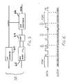
- Fig. 5 is a block diagram showing an alternative embodiment for data transmission between the peripheral and host units of Fig. 1.
- Fig. 6 is an illustration of the data stream and clock signals generated in the peripheral unit and received for synchronous sampling in the host unit in both embodiments.
- System 10 comprises a peripheral unit 12, housed in a peripheral foot pedal unit, that receives state data from a data source 14, such as switches activated by foot pedals on an organ. These switches are also referred to as elements having two states.
- Peripheral unit 12 is coupled to a physically and electrically separated host unit 16, that in turn is coupled to a microprocessor or central processing unit (CPU) 18.
- Host unit 16 transfers power and clock to, and receives synchronous state data from, peripheral unit 12 without interconnecting wires. Further, host unit 16 also translates the state data into transaction data to be sent to host CPU 18.
- Peripheral unit 12 includes a coil 20, that functions as the secondary winding of a power transformer, a clock receiver 22 and a power receiver 24. Both power and a clock signal are derived from the current induced on coil 20.
- a data encoder 26 determines the switch or element state from data source 14, power from power receiver 24, and the clock signal from clock receiver 22. This data encoder serializes data bits representing switch states and interleaves the string of serial data bits with sync and control bits.
- the serialized data stream also referred to as a second data signal, is output to a data transmitter 28.
- data transmission is by infrared emission, as will be described with reference to Fig. 2.
- Host unit 16 includes a power oscillator 30 formed of a power oscillator driver 32, also referred to as means for applying an alternating current to a coil 34.
- Coil 34 functions as a primary coil relative to the power and clock pick-up coil 20 of peripheral unit 12.
- the coils are preferably formed on parallel planar circuit boards with the axes of the coils preferably coaxial. This arrangement allows the coils to be somewhat out of position and still provide magnetic coupling.
- Coil 34 also is the tank coil of oscillator 30. Oscillator 30 is free running and operates in the 20-40kHz range.
- a clock driver 36 rectifies the alternating current signal produced by oscillator 30 to generate a clock signal, synchronous with the clock signal generated by clock receiver 22.
- a preamp/detector 38 translates detected infrared emissions carrying the data stream from data transmitter 28. Detector 38 is also referred to as means for detecting the second data signal.
- the data is then transmitted to a sync detector 40 that monitors the incoming data and resets the count in a bit counter 42 when sync, identifying the start of the data stream, is detected.
- a first memory 44 holds an image of the last known state of the incoming bit stream.
- the data is input to a data comparator 46 that compares the prior data from memory 44 with the incoming data. When the data is different, the data in the memory 44 is replaced with the incoming data, and a strobe on a conductor 48 goes active. Further incoming data is ignored while the output strobe is active.
- Strobe 48 is stored in a CPU interface functioning as a second memory or latch 50.
- the strobe When the strobe is active, it interrupts CPU 18.
- the CPU then reads the data output from bit counter 42 and detector 38 and stored in latch 50, as shown.
- the CPU When the CPU has read the new data information, it causes an acknowledge bit connected to data comparator 46 via a conductor 52 to go active.
- the comparator senses the acknowledge input line as being active, it resets the output strobe to inactive. The CPU will not read the data existing in latch 50 so long as the strobe is in an inactive state.
- Fig. 2 shows the circuit of peripheral unit 12 in further detail.
- Coil 20 is coupled to a combined circuit forming clock receiver 22 and power receiver 24.
- the alternating current existing on coil 20 is rectified by a rectifier 54, filtered by filter 56 and maintained at a 12 volt level by zener diode D2.
- the energy is stored in a capacitor C1.
- the clock is formed from the alternating current signal by a rectifier formed of diodes D4 and D16, which signal is fed into a counter U3 forming part of data encoder 26.
- the power generated and held in capacitor C1 is used to power the components of data encoder 26 and data transmitter 28.
- Encoder 26 includes a couple of matrix switches U1 and U2.
- the low three bits from counter U3 are fed into the enabling inputs of switch U1.
- the upper three bits of counter U3 are fed into the enabling inputs of switch U2.
- This provides for an 8 X 8 switching matrix with the connecting of the X terminal to the XN terminal of U1 to form what may be considered rows of a switch matrix.
- terminal X of switch U2 is selectively connected to the eight XM terminals to form what may be considered columns of a switch matrix.
- one of the XN terminals of switch U1 is connected to one of the XM terminals of switch U2 via a pedal switch 14.
- each XN terminal of switch U1 is connected selectively to each XM terminal of switch U2.
- the two X terminals to switches U1 and U2 are connected through data transmitter circuit 28, which includes a driving transistor Q1 and light emitting diode (LED) D1 for transmission of the data to the host unit 16.
- data transmitter circuit 28 includes a driving transistor Q1 and light emitting diode (LED) D1 for transmission of the data to the host unit 16.
- the switch matrix provides an overall 8 X 8 matrix for generating a 64-bit data stream.
- data encoder 26 encodes the data with sync and control pulses that limit the number of data bits available for the foot pedal switches.
- the X0 terminal of switch U2 is grounded. When this terminal is selected by the appropriate set of enabling inputs, all eight of the corresponding terminals in switch U1 are held low. This forms what is referred to as a sync pulse formed of eight contiguous low pulses. This is used to identify the beginning of the data stream.
- terminal X7 of switch U1 is connected to each of the terminals X1 through X7 of switch U2 through diodes D5-D11. These diodes are always conducting when selected by the matrix switches. They do not sense the state of a pedal switch, as do the other terminal connections. Thus, each eighth bit in the data stream is always high. This guarantees that the only time that eight pulses will appear low is during the sync pulse. There are thus fifteen bits out of the 64-bit data stream that are used for control purposes and are not available for carrying pedal switch state data. A maximum of 49 pedal switches can be sensed with this configuration. It will be recognized that other switch configurations could be used to provide for fewer or more sensing of pedal switches.
- each data stream begins with eight low sync pulses.
- the sync pulses are followed by seven sets of eight data pulses. The first seven of each set of eight data pulses provide pedal switch state data. The eighth pulse always is a high pulse and does not represent switch data.
- another set of sync pulses identify the next stream of data pulses. These sync pulses and high bit pulses are used to verify the validity of the data that is being transmitted from peripheral unit 12 to host unit 16.
- Fig. 4 shows in further detail the circuit schematic associated with host unit 16.
- the infrared data transmitted by data transmitter 28 in peripheral unit 12 is received and sensed by optical receiver U7.
- This receiver detects the data stream, and amplifies and transmits it to sync detector 40 and data comparator 46.
- the data going to the sync detector first passes through an inverter, represented by logic blocks U5A and U6C. This inverter output is connected to the reset of a low bit counter U2 which also receives the clock signal from clock driver 36.
- the clock signal is derived from the alternating current applied to primary transformer windings 34 which form the tank coil for oscillator 30.
- Oscillator driver 32 includes a transistor Q1 and emitter resister R2. The current conducted by the transistor varies according to the loading on coil 34.
- bit counter 42 shown as unit U4 is reset and counts the number of clock pulses. This count identifies the bit number in the data stream associated with the data on line D7 input to latch 50. The bit count associated with that data is represented on the input terminals D0-D6.
- the preceding data stream values have been stored in memory U1 which is a 64-bit shift register. With each clock pulse, each successive value of prior data is output to a data comparator 46 which also receives the new data. Comparator 46 includes an exclusive OR gate that produces a high output only when there is a difference between the old and new data. This comparator output is input into a flip-flop U3A. The flip-flop generates a strobe on conductor 48, as discussed previously, that is stored in latch 50. This strobe is an interrupt to CPU 18. This interrupt tells the CPU that the data value stored on terminal D7, for the position value stored on terminals D0-D6, is new.
- the CPU preferably operates at frequencies much greater than the frequency of the clock signal derived from the sine wave produced by oscillator 30.
- the values are held in latch 50 until the CPU 18 reads them. Once the values are read, an acknowledge signal, identified in Fig. 4 as "taken", is input to latch 50 from the CPU. This signal is used to reset flipflop U3A, which in turn resets the strobe signal to inactive.
- the inverse of the strobe is output from the flip-flop and logically ORed with the 'taken' signal (U5D) inverted again (U6B) and fed to the mode control pin of U1. From the time the signal goes active until the time the 'taken' signal goes active and then inactive again, new data is prevented from being entered into the memory (the old data is recirculated back into the memory).
- Comparator 46 thus acts only for new-versus-old data comparison and does not directly affect data recirculation.
- the recirculation path occurs as stated above, with U1 pin 10 (mode control pin) is active (high). Old data flows from U1 pin 6 back into U1 pin 1 (the recirculate input).
- Register U1 is an image of the data in CPU 18. It thus serves as a separate memory which is independent of the CPU clock. It will be seen that there is thus no timing relationship between the CPU and the circuit of host unit 16. Further, since only transaction data is transmitted to the CPU, data transfer is at typically irregular times.
- data in the form of a clock signal is transferred from primary winding 34 to secondary winding 20.
- Oscillator 30 is made to oscillate at the desired clock rate so that the alternating current signal can be rectified and used as a clock signal for both the components in the peripheral unit and the components in the host unit. This results in synchronous data transmission and reception.
- both power and clock signals are transmitted through the winding coils.
- the infrared transmitter and receiver must be aligned more closely than the coils to provide effective data transmission. This requirement may be overcome by providing data transmission from the peripheral unit to the host unit through the windings as well. In this way, an optical path is not required between the two units. This would allow for placement of opaque materials, such as wood, in between the units and still allow for conductorless data and power transmission.
- the peripheral unit is the same except that diode D1 is not a light emitting diode.
- Encoder 26 by the nature of its operation, loads down or draws power according to the high or low level of the data bits being formed in the data stream. This produces a current in coil 20 that varies in accordance with the data stream. This change in power draw is correspondingly reflected in primary coil 34.
- the current delivered by the oscillator reflects the load presented to the oscillator.
- the data stream is represented by variations in the oscillator current.
- a modified data detection circuit 58 shown in Fig. 5 may be used to detect variations in the oscillator current. In this case, instead of using data transmitter 28, the power receiver 24 and coil 20 serve as the data transmitter.
- the oscillator alternating current signal is input into a clock generator 60 very similar to clock driver 36 shown in host unit 16.
- a signal representative of the current in the emitter resister R2 of power oscillator driver 32, discussed previously, is input into an amplifier or gain block 62.
- This amplified signal is input into a comparator 64 to re-establish the logic levels of the data stream.
- These data logic levels are then fed into a data conditioning circuit 66 to produce a data stream equivalent to the data stream output from preamp/detector 38 in the embodiment of system 10.
- Detection circuit 58 can be seen to provide means for generating a data signal representative of variations in the oscillator current.
- both the clock and the data stream are derived from the alternating current applied to the primary winding 34. These signals are then used in an embodiment which is otherwise the same as that described for host unit 16 with reference to Fig. 4. The data is processed in the same way and fed to the CPU in the same fashion. Thus, except for the differences noted, these embodiments are the same.
- the present invention provides for power and clock signal transmission via the transformer windings in both embodiments with data transmission being alternatively provided through infrared optical means or by the load applied by the peripheral unit on the oscillator through the windings, as has just been described with reference to Fig. 5.
- the present invention provides a connecterless peripheral unit that is easily moved and which eliminates possible damage due to the existence of a physical connector or cable. Transferring power and data between the peripheral and host units by either of the embodiments reduces physical alignment problems often associated with the other methods.
- the physical alignment requirements associated with the embodiment of Fig. 5, not including the infrared transmission link, are less rigid than that with the embodiment shown with reference to Figs. 2 and 3.
- the embodiment of Fig. 5 also provides for the insertion of opaque materials completely between the two units while still providing for power, clock and state data information transfer.
- the power oscillator By using the power oscillator also as the data clock allows both units to have a common clock, thereby providing synchronous data transfer without requiring an additional communication channel.
- the power oscillator does double duty.
- it does triple duty by also providing data transfer from the peripheral unit to the base or host unit.
- a high degree of confidence in data integrity of contiguous state data is maintained by testing for the presence of the sync bit. Loss of sync provides an indication of the removal or failure of the peripheral. Transferring continuous state data instead of transaction data from the peripheral unit to the host unit has the advantages of simpler data encoding and decoding. Then, transfer of transaction data to the CPU reduces CPU service time since only changes in state require attention of the CPU.
- Using a free-running oscillator instead of one generated by the CPU further simplifies circuit topology for generation of a sinusoidal waveform, thus reducing RFI emissions.
- the oscillator may operate at any convenient frequency. The frequency of oscillation is chosen low enough so as to discourage radio interference, but high enough to maximize the efficiency for the coil type used, and high enough to allow timely servicing of the input data.
Landscapes
- Physics & Mathematics (AREA)
- General Physics & Mathematics (AREA)
- Near-Field Transmission Systems (AREA)
Applications Claiming Priority (2)
| Application Number | Priority Date | Filing Date | Title |
|---|---|---|---|
| US47760090A | 1990-02-09 | 1990-02-09 | |
| US477600 | 2000-01-04 |
Publications (1)
| Publication Number | Publication Date |
|---|---|
| EP0441492A2 true EP0441492A2 (en) | 1991-08-14 |
Family
ID=23896594
Family Applications (1)
| Application Number | Title | Priority Date | Filing Date |
|---|---|---|---|
| EP91300440A Withdrawn EP0441492A2 (en) | 1990-02-09 | 1991-01-21 | System and method for transferring data |
Country Status (2)
| Country | Link |
|---|---|
| EP (1) | EP0441492A2 (ja) |
| JP (1) | JPH04213929A (ja) |
-
1991
- 1991-01-21 EP EP91300440A patent/EP0441492A2/en not_active Withdrawn
- 1991-02-08 JP JP3018083A patent/JPH04213929A/ja not_active Withdrawn
Also Published As
| Publication number | Publication date |
|---|---|
| JPH04213929A (ja) | 1992-08-05 |
Similar Documents
| Publication | Publication Date | Title |
|---|---|---|
| US4569045A (en) | 3-Wire multiplexer | |
| JPS6084687A (ja) | Icカ−ドの処理方法および装置ならびにicカ−ド | |
| CA2036378A1 (en) | Proximity detecting apparatus | |
| EP0689737A1 (en) | Inductively coupled keyboard | |
| EP0441492A2 (en) | System and method for transferring data | |
| CN209044562U (zh) | 指纹识别装置与智能终端 | |
| US5001705A (en) | Protocol control circuit for data bus system | |
| JPS61103297A (ja) | 電子複写機制御装置 | |
| CN100358290C (zh) | 医疗设备使用漏费控制系统 | |
| JPH05233127A (ja) | コードレスデジタイザ | |
| US5714720A (en) | High efficiency passive pointer digitizer system | |
| JPS62147599A (ja) | 空間送受信型検針器 | |
| JPH04326415A (ja) | ワイヤレスキーボード装置 | |
| JP3507380B2 (ja) | 電流搬送送信器 | |
| JPH04370820A (ja) | デジタイザ | |
| JPS6150436A (ja) | 電力線搬送制御システム | |
| JP2986821B2 (ja) | 座標検出装置 | |
| JPS6195646A (ja) | 停電検出方式 | |
| JP2712304B2 (ja) | データ伝送方法,データ伝送装置,データ受信方法およびデータ受信装置 | |
| Stairs et al. | Design Options for an SSC Wire Chamber Data Collection System | |
| JP3585553B2 (ja) | 光送受信モジュール | |
| JPS61105148A (ja) | デ−タ収集システム | |
| JPH05268673A (ja) | リモコン装置 | |
| JPH02200096A (ja) | 信号伝送システム | |
| JPS6313225B2 (ja) |
Legal Events
| Date | Code | Title | Description |
|---|---|---|---|
| PUAI | Public reference made under article 153(3) epc to a published international application that has entered the european phase |
Free format text: ORIGINAL CODE: 0009012 |
|
| AK | Designated contracting states |
Kind code of ref document: A2 Designated state(s): DE GB IT NL |
|
| 18W | Application withdrawn |
Withdrawal date: 19911205 |
|
| STAA | Information on the status of an ep patent application or granted ep patent |
Free format text: STATUS: THE APPLICATION HAS BEEN WITHDRAWN |
|
| R18W | Application withdrawn (corrected) |
Effective date: 19911205 |