EP0441706A1 - Rechner für Flugkörper - Google Patents
Rechner für Flugkörper Download PDFInfo
- Publication number
- EP0441706A1 EP0441706A1 EP91400289A EP91400289A EP0441706A1 EP 0441706 A1 EP0441706 A1 EP 0441706A1 EP 91400289 A EP91400289 A EP 91400289A EP 91400289 A EP91400289 A EP 91400289A EP 0441706 A1 EP0441706 A1 EP 0441706A1
- Authority
- EP
- European Patent Office
- Prior art keywords
- computer
- circuit
- memory
- bus
- processor
- Prior art date
- Legal status (The legal status is an assumption and is not a legal conclusion. Google has not performed a legal analysis and makes no representation as to the accuracy of the status listed.)
- Granted
Links
- 230000015654 memory Effects 0.000 claims abstract description 88
- 238000012545 processing Methods 0.000 claims abstract description 40
- 230000008878 coupling Effects 0.000 claims abstract description 38
- 238000010168 coupling process Methods 0.000 claims abstract description 38
- 238000005859 coupling reaction Methods 0.000 claims abstract description 38
- 230000005540 biological transmission Effects 0.000 claims abstract description 21
- 238000004364 calculation method Methods 0.000 claims abstract description 10
- 230000009977 dual effect Effects 0.000 claims description 10
- 210000000056 organ Anatomy 0.000 claims description 6
- 238000011282 treatment Methods 0.000 claims 1
- 230000004044 response Effects 0.000 description 16
- 239000000872 buffer Substances 0.000 description 11
- 238000010586 diagram Methods 0.000 description 8
- 238000010304 firing Methods 0.000 description 7
- 238000013475 authorization Methods 0.000 description 6
- 238000000034 method Methods 0.000 description 6
- 238000004891 communication Methods 0.000 description 5
- 230000006870 function Effects 0.000 description 5
- 230000006978 adaptation Effects 0.000 description 4
- 230000002457 bidirectional effect Effects 0.000 description 4
- 230000008859 change Effects 0.000 description 4
- 238000006243 chemical reaction Methods 0.000 description 4
- 235000021183 entrée Nutrition 0.000 description 4
- 230000005764 inhibitory process Effects 0.000 description 4
- 238000010200 validation analysis Methods 0.000 description 4
- 101100255642 Arabidopsis thaliana RTE1 gene Proteins 0.000 description 3
- 101000848490 Homo sapiens Putative RNA polymerase II subunit B1 CTD phosphatase RPAP2 Proteins 0.000 description 3
- 102100034621 Putative RNA polymerase II subunit B1 CTD phosphatase RPAP2 Human genes 0.000 description 3
- 238000000429 assembly Methods 0.000 description 3
- 238000005516 engineering process Methods 0.000 description 3
- 238000004519 manufacturing process Methods 0.000 description 3
- 101100255666 Saccharomyces cerevisiae (strain ATCC 204508 / S288c) RTR2 gene Proteins 0.000 description 2
- 239000000470 constituent Substances 0.000 description 2
- 238000011161 development Methods 0.000 description 2
- 238000007667 floating Methods 0.000 description 2
- 238000010438 heat treatment Methods 0.000 description 2
- 238000002513 implantation Methods 0.000 description 2
- 238000009434 installation Methods 0.000 description 2
- 230000004048 modification Effects 0.000 description 2
- 238000012986 modification Methods 0.000 description 2
- 230000002829 reductive effect Effects 0.000 description 2
- 238000003860 storage Methods 0.000 description 2
- 239000000725 suspension Substances 0.000 description 2
- 230000001360 synchronised effect Effects 0.000 description 2
- 238000012360 testing method Methods 0.000 description 2
- 230000009849 deactivation Effects 0.000 description 1
- 230000001934 delay Effects 0.000 description 1
- 238000001514 detection method Methods 0.000 description 1
- 230000002401 inhibitory effect Effects 0.000 description 1
- 230000010354 integration Effects 0.000 description 1
- 238000012432 intermediate storage Methods 0.000 description 1
- 238000005259 measurement Methods 0.000 description 1
- 230000008520 organization Effects 0.000 description 1
- 244000045947 parasite Species 0.000 description 1
- 230000003071 parasitic effect Effects 0.000 description 1
- 230000008569 process Effects 0.000 description 1
- 230000000135 prohibitive effect Effects 0.000 description 1
- 230000001141 propulsive effect Effects 0.000 description 1
- 230000001869 rapid Effects 0.000 description 1
- 230000000717 retained effect Effects 0.000 description 1
- 230000002441 reversible effect Effects 0.000 description 1
- 230000033764 rhythmic process Effects 0.000 description 1
- 238000000926 separation method Methods 0.000 description 1
- 238000012163 sequencing technique Methods 0.000 description 1
- 238000007493 shaping process Methods 0.000 description 1
- 238000012546 transfer Methods 0.000 description 1
- 230000009466 transformation Effects 0.000 description 1
- 230000001960 triggered effect Effects 0.000 description 1
Images


Classifications
-
- G—PHYSICS
- G05—CONTROLLING; REGULATING
- G05D—SYSTEMS FOR CONTROLLING OR REGULATING NON-ELECTRIC VARIABLES
- G05D1/00—Control of position, course, altitude or attitude of land, water, air or space vehicles, e.g. using automatic pilots
- G05D1/10—Simultaneous control of position or course in three dimensions
- G05D1/107—Simultaneous control of position or course in three dimensions specially adapted for missiles
Definitions
- the present invention relates to a missile computer.
- the main function of a missile computer is automatic piloting of the missile. As such, it performs the calculations necessary for navigation, piloting and guidance of the missile, and it adapts and manages the necessary input / output information for this purpose.
- the computer participates in the firing and flight sequence, and it collects and sends to a telemetry link the parameters retained for the measurement plan.
- the object of the present invention is to propose a missile computer architecture giving it greatly increased processing power while respecting such conditions.
- This particular architecture of the computer provides the desired increase in processing power, without increasing the volume, in particular by using integrated circuits with very large scale integration (VLSI), and with reduced consumption and heating, in particular by using CMOS technology.
- VLSI very large scale integration
- a missile 1 may comprise, from front to rear, a self-steering device 2, an inertial unit with a sensor block 3, a load 4, a proximity rocket 5, a computer 6 and a propulsion system 7.
- the latter can comprise at least one axial propulsion nozzle which can be oriented, or not, and lateral pilot nozzles.
- Adjustable aerodynamic control surfaces 8 are fixed to the body of the missile. In this example, each of the components 1 to 6 of the missile occupies a section thereof.
- the computer 6 mainly performs the calculations necessary for navigation, piloting and guiding the missile. To this end, the computer 6 receives in particular information coming from a firing or control station and received by a radar missile link receiver (not shown in FIG. 1), as well as information supplied by the self-steering device 2 (when the target has been "hooked") and the sensor unit 3, and information supplied by sensors and representative of the nozzle (s) and control surfaces positions. The computer provides information for controlling the position of the nozzle (s) and control surfaces and control information for the proximity rocket 5.
- the computer 6 also prepares telemetry information which is transmitted to the firing or control center and which represents a certain number of predetermined parameters.
- the computer 6 also takes part in the firing sequence.
- FIG. 2 A functional diagram of the computer 6 is illustrated in FIG. 2.
- the computer 6 essentially comprises a central unit 10, memory circuits 20 associated with the central unit, an algorithmic processing unit 30, a serial coupling circuit 40 connecting the computer to external serial digital data buses, a circuit for parallel coupling 50 connecting the computer to an external parallel digital bus, an analog / digital (A / D) and digital / analog (D / A) conversion circuit 60 connecting the computer to external analog connections and an adaptation circuit 70 of discrete signals connecting the computer to external analog connections.
- a / D analog / digital
- D / A digital / analog
- the central unit 10 (FIG. 3) is organized around a microprogrammable processor 11. It further comprises a microprogram memory 12 and a circuit 13 for managing time and interrupts; both connected to the central unit 10.
- the central unit 10 is responsible for managing the tasks performed by the computer, managing the input / output information from and to the buses and external links and the exchanges with the algorithmic processing unit 30.
- the processor 11 is a processor of the microprogrammable type preferably produced in CMOS technology in order to minimize consumption and heating.
- the processor 11 and the circuit 13 are connected to a bus 15 which comprises a data bus 15D, for example on 16 bits, an address bus 15A, for example also on 16 bits, and a control bus 15C, for example on 10 bits.
- the internal bus 80 of the computer is an extension of bus 15 of the central unit.
- circuit 13 The functions of circuit 13 are the generation of basic clock signals from the computer, the generation of real-time clock signals, the management of interruptions and tasks and the arbitration of access to the internal bus of the computer.
- the circuit 13 can be produced in the form of a specific integrated circuit.
- the structure of the central unit 10 is therefore entirely conventional, so that a more detailed description is not necessary here.
- the memory circuits 20 include a random access memory (RAM) 21, an application memory 22 of the PROM type and a memory management circuit 23.
- the memory space is divided into sheets, these being two in number (F0, F1) in the example illustrated.
- the address of a word in memory includes the number of the selected sheet, number indicated by a sheet register which is loaded by the central unit and which is part of the circuit 23, and the 15 least significant bits of the bus d addresses, which are stored in an address register forming part of the circuit 23.
- the sheet F0 constitutes the private memory of the processor 11 of the central unit and is divided into a first part constituting the private random access memory RAM and a second part constituting the private memory PROM.
- the latter contains the application programs implemented by the central unit.
- Other application programs are stored in PROM memory in the algorithmic processing unit for the operations carried out by the latter.
- the sheet F1 comprises two RAM memory segments, one forming an exchange memory with the algorithmic processing unit, the other forming an exchange memory with the coupling circuits.
- the exchange zones are in the address field but not interlaced; alignment is done by the compiler.
- the memory is of the interleaved type to be able to present two bytes simultaneously on the data bus 15D, although the central unit addresses bytes.
- the memory space is divided into an even memory containing all the bytes of even address and an odd memory containing all the bytes of odd address.
- FIG. 5 shows in detail an embodiment of the management circuit 23 and of the memories managed by this circuit.
- the RAM memory 21, which in particular constitutes the sheet F1 is divided into an even memory 21P and an odd memory 21I which can be constituted by separate circuits.
- the PROM memory 22, which is part of the sheet F0 is divided into an even memory 22P and an odd memory 22I.
- the management circuit 23 comprises a sheet management circuit 231 which includes a sheet register in which the number of the selected sheet is loaded. The change is made with the value delivered by the bit D (0) of the data bus 15D under the control of a signal produced by a decoding circuit 232 in response to a micro-order transmitted in a field of the control bus 15C , for example field A (0: 3).
- the decoding circuit 232 also receives a validation signal VA or field A from the central unit.
- the sheet management circuit can manage a number of sheets greater than two.
- the number of the selected sheet will then be given by two bits D (0: 1), or more if necessary, of the data bus 15D.
- Circuit 234 receives bytes transmitted on the DP (0: 7) and DI (0: 7) data buses assigned to the even and odd memories, respectively, and distributes them in LSB or MSB position on the data bus 15D.
- Circuit 235 receives the LSB and MSB bytes and distributes them on the DP (0: 7) or DI (0: 7) buses.
- the circuits 234 and 235, as well as gates connected at the output of these circuits, are controlled by a control circuit 236 in response to the decoding, by the circuit 232, of micro-orders for reading or writing on a byte or two. bytes.
- the circuit 236 In response to the micro-orders decoded by the circuit 232 and according to the parity of the address, the circuit 236 also provides signals OEPP, OERP, WERP of authorization to read in memory PROM pair, of authorization to read in RAM memory pair and authorization to write in RAM pair, as well as OEPI, OERI and WERI signals for authorization to read from odd PROM memory, authorization to read from odd RAM and authorization to write to memory Odd RAP.
- the operation of the constituent circuits of the management circuit 23 is synchronized by a clock circuit 237 receiving clock signals from the central unit.
- the function of the algorithmic processing unit 30 is to perform calculations very quickly and in floating point.
- the processing unit 30 (FIG. 6) is for example formed by a coprocessor using a processor 31 of the "29000” type associated with a floating point accelerator processor 32 of the "29027” type, both of which are sold by the departments desettes - United States of America “AMD" ("Advanced Micro Devices").
- the processing unit 30 further comprises its own memories addressed by the coprocessor 31-32: a random access memory 33 (RAM) and a program memory 34 (PROM).
- RAM random access memory
- PROM program memory 34
- the latter contains the programs necessary for the execution of the processing operations by the coprocessor and provides the instructions corresponding thereto.
- These processing operations consist essentially of conventional navigation guidance and piloting calculations to provide control surface control information from information supplied by the self-steering system and the sensor unit and those received by the missile radar link.
- the dialogue between the algorithmic processing unit 30 and the central unit 10 takes place via a dual-access exchange memory 35 interposed between the bus of the coprocessor 31-32 and the internal bus 80 of the computer.
- a circuit 36 manages access to the exchange memory 35 for reading and writing.
- the function of the coupling circuit 40 (FIG. 7) is to couple the computer to serial links, in this case a bus 41 and a link 42.
- a bus 41 connects the computer to the missile radar link receiver, and to the on-board telemetry transmitter.
- the bus 41 is also used for the connection with the firing installation.
- the bus 41 is for example a two-wire serial bus of the "1553" type.
- the link 42 connects the computer to the proximity rocket 5.
- the link 42 is for example a simple bidirectional digital asynchronous link of RS232 type for the procedure and of RS422 type for the physical layer.
- the coupling circuit 40 is an "intelligent" coupler organized around a microprogrammable processor 43 preferably produced in CMOS technology.
- the processor 43 functions as a microprogrammed arithmetic and logic automaton receiving instructions from a microprogram memory 44.
- the communication procedures on the bus 41 and the link 42 and the exchange procedures with the processing unit 10 are contained in memory 44.
- the coupling circuit 40 also includes a random access memory (RAM) 45, an erasable and rewritable non-volatile memory (EEPROM) 46, and a logic circuit 47 connected to circuits 410 and 420 forming an interface with the bus 41 and the link 42.
- RAM random access memory
- EEPROM erasable and rewritable non-volatile memory
- the memories 45, 46 and the logic circuit 47 are coupled to the data bus 48D and to the address bus 48A of the processor 43.
- the non-volatile memory 46 is used to store the frame of the parameters sent to the telemetry. This memory is loaded at manufacturing stage via the bus 41 using a microprogrammed procedure contained in the memory 44. Thus, the frame of the parameters to be telemetered can it be easily changed from one manufacturing to another. In addition; if a modification of the parameter frame is desired, for example during a test campaign, this modification can very simply be carried out by erasing and rewriting in the memory 46 under the control of the processor 43.
- the random access memory 45 is used for the microprogrammed processing carried out by the processor 43. It can also be used as backup memory when the processor is interrupted.
- the logic circuit 47 ensures the serialization of the information to be transmitted on the bus 41 and the link 42, as well as the decoding and the deserialization of the information received from the bus 41 and the link 42. To this end, the logic circuit 47 comprises registers buffers for intermediate storage of information. In addition, the logic circuit 47 receives clock signals from a time base 43A which also provides the clock signals necessary for the operation of the processor 43. The circuit 47 is still connected to the control bus 48C of the processor 43 and to the control bus forming part of the bus 80, this in order to receive micro-orders transmitted on this latter control bus from the central unit.
- the dialogue between the coupling circuit 40 and the processing unit 10 is carried out by means of a dual access exchange memory 49. This is connected, on one side, to the internal bus 80 of the computer. and, on the other hand, to the data buses 48D and addresses 48A of the processor 43.
- FIG. 8 shows in more detail an embodiment of the logic circuit 47.
- the circuit 47 essentially comprises: a first serial line circuit 470 interposed between the buses 48D, 48A and 48C of the processor 43 and the interface circuit 410, a second serial line circuit 471 interposed between the buses 48D, 48A, and 48C and the interface circuit 420, a circuit 472 for triggering a military charge, a bidirectional amplifier (buffer) 473 interposed between the data bus of the bus 80 and the data bus 48D, a decoding circuit 474 interposed between the control bus of the bus 80 and the control bus 48C, and a circuit 475 for triggering a military charge.
- a bidirectional amplifier (buffer) 473 interposed between the data bus of the bus 80 and the data bus 48D
- decoding circuit 474 interposed between the control bus of the bus 80 and the control bus 48C
- a circuit 475 for triggering a military charge.
- the bidirectional amplifier (buffer) 473 is controlled by the control bus 48C.
- the decoding circuit 474 receives micro-commands transmitted on the control bus of the bus 80, from the central unit 10, and decodes them to transmit the corresponding commands on the control bus 48C.
- Line circuit 470 essentially performs parallel / serial transformation, coding / decoding and detection of transmission errors. It includes two transmission registers RTE1 and RE1, two reception registers RR1 and RTR1, a coding / decoding circuit CDC, a status register RST, a control register RCT, a clock circuit CLK and a logic circuit CTL control.
- the transmission register RTE1 is a buffer register in which the storage is controlled by the circuit CTL, and which is interposed between the data bus 48D and the parallel input of the transmission register RE1 with parallel input and serial output. The latter is connected to the coding input of the CDC circuit.
- the reception register RTR1 is a buffer register in which the storage is also controlled by the circuit CTL, and which is interposed between the parallel output of the reception register RR1 with serial input and parallel output and the data bus 48D.
- the serial input of the RE register is connected to the decoding output of the CDC circuit.
- the coding / decoding circuit CDC converts the parallel data supplied on the bus 48D into serial data coded according to the standard of the bus 41 of type "1553".
- the CDC circuit includes a protection circuit which inhibits transmission when a transmission exceeds a predetermined duration.
- the CDC circuit includes a filter intended to eliminate the spurious signals and a decoder ensuring the conversion of the serial data coded according to the "1553" standard into words usable by the processor 43.
- the CLK clock circuit makes it possible to date the response times of the subscribers connected to the bus 41. It includes a counter incremented by a clock signal originating from the time base 43A and a register preloaded from the bus 48D data, under the control of the CTL circuit.
- the register is preloaded to a value corresponding to a predetermined maximum response time.
- the counter is triggered in response to a signal from the CDC circuit when a word is transmitted and stopped in response to a signal from the CDC circuit when a word is received.
- the exceeding by the counter of the value preloaded in the register commands an interruption towards the processor 43.
- the control logic circuit CTL decodes the words received from the control bus 48C and from the address bus 48A to generate the control signals from the buffer registers RTE1, RTR1, from the control register RCT and from the status register RST and from the circuit CLK clock.
- the TX transmission outputs and RX reception inputs of the CDC circuit, as well as a TXINH output for inhibiting transmission are connected to the interface circuit 410 which comprises a transmitter / receiver 411 and a transformer 412 connected to the two-wire bus. 41.
- the bus 41 Before launching the missile, the bus 41 is connected to the bus of the same type of the firing installation by means of contacts of a relay 415, the opening of which is caused by a control circuit 416 in response to the change in state of one of the bits of the control word contained in the register RCT. It is by this link that, if necessary, the frame of the telemetered parameters can be modified in the EEPROM memory 46 before a test.
- the bus 41 puts the computer in communication with the missile radar link and the telemetry transmitter. All the data likely to be sent to telemetry are stored in the dual access exchange memory 49 coming from the central unit 10 or from the algorithmic processing unit 30.
- the EEPROM memory 46 contains the addresses of the data to be measured and the profile of the frame in which this data is to be transmitted.
- the serial line circuit 471 includes an RTD data buffer register interposed between the 48D data bus and an internal BDI data bus. To this latter are connected a control and status register RCE, a transmission buffer register RTE2 and a reception buffer register RTR2. A transmission register RE2 with parallel inputs and serial output is inserted between the buffer register RTE2 and the interface circuit 420 while a reception register RR2 with serial input and parallel outputs is inserted between the interface circuit 420 and the buffer register RTR2. These different registers of the serial line circuit 471 are controlled by a read-write control circuit (CRW) which is connected to the control buses 48C and of addresses 48A and is connected to the time base 43A.
- CCW read-write control circuit
- the serial line circuit 471 described above is conventional, as are the interface circuits 420 via which they are connected to the bus 42. They may for example be constituted, respectively, by the circuits referenced 26 LS 31 and 26 LS 32 from companies in the United States of America MOTOROLA or TEXAS INSTRUMENTS.
- the military load trigger logic circuit 475 produces the DCM signal for triggering the load driven by the missile. To this end, it receives discrete signals (all or nothing) from the proximity rocket. These validate a countdown circuit which is preloaded from the bus 48D to values corresponding to tripping delays calculated by the central unit and which counts down to the rhythm of a clock signal originating from the time base 43 .
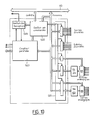
- the parallel coupling circuit 50 (FIG. 9) connects the computer to the self-directing device 2 and to the sensor unit 3 via a parallel bus 51, for example with 8 bits, which is managed by the computer.
- the parallel coupling circuit is of the microprogrammed type, the procedure being contained in the firmware memory of the processor 11.
- the electronic and interface circuits with the bus 80, constituting the coupler 50, can be grouped in an integrated circuit.
- the conversion circuit 60 comprises an analog / digital converter circuit 61 and a digital / analog converter circuit 62.
- the incoming analog signals are in particular representative of the actual positions of control surfaces and of nozzle, and of battery voltage values, while the signals outgoing analogs are in particular representative of the control and nozzle setpoint positions.
- Circuits 63, 64 constituted by operational amplifiers, ensure the adaptation and scaling of the analog signals.
- the computer also processes discrete input and output signals, the discrete incoming signals are for example indicative of output from the launch tube, separation of the first stage (in the case of a missile with several propulsive stages), reset. ..
- the discrete outgoing signals are in particular firing orders for power stacks, the cruise booster or a gas generator supplying lateral nozzles allowing piloting.
- the adaptation and scaling of the discrete incoming and outgoing signals are carried out by means of the adaptation circuit 70 using operational amplifiers.
- the constituent elements of the parallel coupling circuit 50 and of the circuits for managing the incoming and outgoing analog and discrete signals can be grouped in the same integrated circuit 52, the block diagram of which is given in FIG. 10.
- the sequencing of the sub-assemblies is ensured by clock signals supplied by the central unit and received by the command management sub-assembly 522.
- the latter is connected to the control bus forming part of the bus 80, in order to receive micro-orders via the control field of the processor of the central unit.
- micro-orders make it possible, after decoding, to generate the commands contributing to the management of exchanges and interruptions: validation of the inputs-outputs, propagation of functional data, shaping of the external signals necessary for this propagation.
- the interrupt management sub-assembly 523 is connected to the parallel coupler 520 in order to send a suspension signal to the processor 11 of the central unit in response to an interrupt request from a subscriber of the bus 51 (sensor block or self-director).
- the processor 11 then sends to the then to the sub-assembly 522 a micro-order authorizing the reading in the parallel coupler 520 bits identifying the subscriber who requested the suspension. These bits are contained in a control word stored in a register of the parallel coupler and are read on the data bus of the central unit 10, forming part of the bus 80 and connected to the parallel coupler 520.
- the latter is connected to the bidirectional parallel bus 51. It also transmits, to the subscribers, a clock signal, a signal indicating the presence of a control word on the bus 51 and a signal indicating the presence of a word data on the bus 51.
- the writing of a control word, the writing of data and the reading of data on the bus 51 are carried out under the control of the subassembly 522 in response to micro-orders received from central unity.
- the input-output subset 521 is connected to the discrete and analog inputs and outputs and to the data bus of the bus 80.
- the discrete inputs have their states stored in respective positions of a register of the subset 521 which is read on the data bus forming part of the bus 80 in response to a micro-order transmitted by the central unit and decoded by the subset 522.
- the discrete outputs have their states determined by bits stored in respective positions of a register of the subset 521 which is loaded from the data bus forming part of the bus 80 in response to a micro-order. transmitted by the central unit and decoded by the subassembly 522.
- the analog inputs are multiplexed by means of a multiplexer 65 at the input of the A / D converter 61.
- the analog channel to be read is selected by command of the multiplexer 65 by a word stored in a register of the subset 521 in response to a microphone. -order transmitted by the central unit and decoded by the subassembly 522.
- the conversion of the analog data and the reading of the converted data, at the output of the converter are then successively controlled in response to micro-orders transmitted by the central unit and decoded by subset 522.
- the converted data read is transferred to a register of the sub-assembly 522 to be transmitted on the data bus forming part of the bus 80.
- the analog outputs are demultiplexed at the output of the D / A converter 62 by means of a demultiplexer 66.
- a register of the sub-assembly 521 stores a word of which a part constitutes the address of the analog channel to be activated and another part the value digital analog output signal to be transmitted on this channel. This word is read on the data bus forming part of the bus 80, in response to a micro-order transmitted by the central unit and decoded by the sub-assembly 522.
- FIG. 11 shows the exchanges between the sub-assemblies of the computer and the interruption lines (in broken lines) between these sub-assemblies.
- the series 40 coupling circuit allows the computer to communicate with telemetry, the missile radar link and the proximity rocket.
- the exchange of data between the central unit 10 and these three organs is carried out by means of the dual access memory 49.
- the data are recorded therein and the synchronization between the central unit 10 and the coupling circuit series 40 is performed by interruptions.
- interruptions are available from the central unit 10 to the coupling circuit 40: interruption of start of exchange with the serial bus 41 (IT start of exchange bus 41), interruption of transmission of parameters to telemetry (IT transmission of telemetry plan ) and interruption of transmission to the proximity rocket (IT transmission to FP).
- interruption of start of exchange with the serial bus 41 interruption of start of exchange bus 41
- interruption of transmission of parameters to telemetry interruption of transmission of telemetry plan
- interruption of transmission to the proximity rocket interruption of transmission to the proximity rocket
- Three interruptions are sent by the coupling circuit 40 to the central unit 10: end of exchange interruption with bus 41 (IT end of bus exchange 41), reception interruption from the proximity rocket (IT reception FP) and error interrupt on bus 41 or change of frame of parameters to be telemetered (IT bus error 41 or telemetry frame change).
- the central unit 10 Communication between the central unit 10 and the algorithmic processing unit 30 takes place in a similar manner.
- the data is exchanged via the dual access memory 35.
- the tasks of the unit 30 represent all of the guidance, piloting and navigation processing. They are synchronized with three external events: reception of data from the sensor unit, reception of data from the self-steering device and reception of data from the missile radar link.
- the first two events have a frequency for example of 500 Hz and the third a frequency for example of 1 Hz.
- Each of these events is associated with an interruption, respectively IT AD, IT BS and IT LRM.
- two interruptions are available by decoding the address bus when writing to the dual access memory. These two interruptions are a functional results interruption (functional IT results) and a telemetry interruption (IT telemetry).
- a specific instruction could be provided for the processing unit making it possible to transfer data directly from the dual access memory 35 of the processing unit 30 to the dual access memory 49 of the coupling circuit 40, and vice versa.
- results of calculations carried out by the processing unit 30, and representing parameters to be telemetered can be transmitted directly to the coupling circuit 40, for transmission on the bus 41, while data coming from the radar link missile via bus 41 can be transmitted directly to processing unit 30.
- the parallel bus 51 makes it possible to communicate with the self-directing device 2 and the sensor block 3.
- the data coming from the bus 51 is stored directly, by the management firmware of the parallel coupling circuit, in the dual access memory 35, to be used in the calculations made by the processing unit 30, or in the dual access memory 49, to be transmitted to the telemetry.
- the inputs / outputs for discrete and analog signals allow the exchange of data and commands with various missile elements: control surfaces, batteries, pilot nozzles, proximity rocket ... They are read and recorded under the control of the unit processing 10 by specific instructions which exchange data with input / output registers addressed by micro-orders.
Landscapes
- Engineering & Computer Science (AREA)
- Aviation & Aerospace Engineering (AREA)
- Radar, Positioning & Navigation (AREA)
- Remote Sensing (AREA)
- Physics & Mathematics (AREA)
- General Physics & Mathematics (AREA)
- Automation & Control Theory (AREA)
- Radar Systems Or Details Thereof (AREA)
- Control By Computers (AREA)
- Aiming, Guidance, Guns With A Light Source, Armor, Camouflage, And Targets (AREA)
- Hardware Redundancy (AREA)
Applications Claiming Priority (2)
| Application Number | Priority Date | Filing Date | Title |
|---|---|---|---|
| FR9001479A FR2657980B1 (fr) | 1990-02-08 | 1990-02-08 | Calculateur de missile. |
| FR9001479 | 1990-02-08 |
Publications (2)
| Publication Number | Publication Date |
|---|---|
| EP0441706A1 true EP0441706A1 (de) | 1991-08-14 |
| EP0441706B1 EP0441706B1 (de) | 1995-05-10 |
Family
ID=9393508
Family Applications (1)
| Application Number | Title | Priority Date | Filing Date |
|---|---|---|---|
| EP91400289A Expired - Lifetime EP0441706B1 (de) | 1990-02-08 | 1991-02-07 | Rechner für Flugkörper |
Country Status (4)
| Country | Link |
|---|---|
| EP (1) | EP0441706B1 (de) |
| DE (1) | DE69109512T2 (de) |
| ES (1) | ES2074669T3 (de) |
| FR (1) | FR2657980B1 (de) |
Cited By (1)
| Publication number | Priority date | Publication date | Assignee | Title |
|---|---|---|---|---|
| FR2833722A1 (fr) * | 2001-12-18 | 2003-06-20 | Thales Sa | Procede d'optimisation de l'interception de cibles mobiles, systeme d'interception et missile mettant en oeuvre un tel procede |
Citations (2)
| Publication number | Priority date | Publication date | Assignee | Title |
|---|---|---|---|---|
| US4037202A (en) * | 1975-04-21 | 1977-07-19 | Raytheon Company | Microprogram controlled digital processor having addressable flip/flop section |
| EP0200352A2 (de) * | 1985-03-25 | 1986-11-05 | British Aerospace Public Limited Company | Steuerungssystem mit Rechner |
-
1990
- 1990-02-08 FR FR9001479A patent/FR2657980B1/fr not_active Expired - Fee Related
-
1991
- 1991-02-07 ES ES91400289T patent/ES2074669T3/es not_active Expired - Lifetime
- 1991-02-07 EP EP91400289A patent/EP0441706B1/de not_active Expired - Lifetime
- 1991-02-07 DE DE69109512T patent/DE69109512T2/de not_active Expired - Fee Related
Patent Citations (2)
| Publication number | Priority date | Publication date | Assignee | Title |
|---|---|---|---|---|
| US4037202A (en) * | 1975-04-21 | 1977-07-19 | Raytheon Company | Microprogram controlled digital processor having addressable flip/flop section |
| EP0200352A2 (de) * | 1985-03-25 | 1986-11-05 | British Aerospace Public Limited Company | Steuerungssystem mit Rechner |
Non-Patent Citations (1)
| Title |
|---|
| IEEE Computer Society: Proceedings Real-Time Systems Symposium, 6-8 Décembre 1988 Huntsville, Alabama US pages 60 - 68; R. Bond et al.: "Missile Guidance Processor Software Development: A Case Study" * |
Cited By (2)
| Publication number | Priority date | Publication date | Assignee | Title |
|---|---|---|---|---|
| FR2833722A1 (fr) * | 2001-12-18 | 2003-06-20 | Thales Sa | Procede d'optimisation de l'interception de cibles mobiles, systeme d'interception et missile mettant en oeuvre un tel procede |
| WO2003054647A1 (fr) * | 2001-12-18 | 2003-07-03 | Thales | Procede d'optimisation de l'interception de cibles mobiles, systeme d'interception et missile mettant en oeuvre un tel procede |
Also Published As
| Publication number | Publication date |
|---|---|
| FR2657980B1 (fr) | 1992-05-29 |
| FR2657980A1 (fr) | 1991-08-09 |
| DE69109512D1 (de) | 1995-06-14 |
| ES2074669T3 (es) | 1995-09-16 |
| EP0441706B1 (de) | 1995-05-10 |
| DE69109512T2 (de) | 1995-10-05 |
Similar Documents
| Publication | Publication Date | Title |
|---|---|---|
| US4700292A (en) | Interface circuit arrangement for transferring data from a master processor to a slave processor | |
| US9455938B2 (en) | Streaming methods and systems for network devices | |
| FR2925191A1 (fr) | Architecture de traitement numerique a haute integrite a multiples ressources supervisees | |
| EP0807935B1 (de) | Gleichzeitiges Lese- und Schreibeverfahren von Daten in einem RAM-Speicher | |
| IE842855L (en) | Buffer system for input-output portion of digital data¹processing system | |
| CA2186449A1 (en) | Bandwidth Management and Access Control for an ATM Network | |
| EP0725554A3 (de) | Methode und Apparat für Vermittlung, Mehrfachsendeverfahren, Multiplexierung und Demultiplexierung einer ATM-Zelle | |
| US8186588B2 (en) | Shared drive launcher/weapon interface | |
| FR2679352A1 (fr) | Dispositif universel de couplage d'un bus d'ordinateur a un controleur d'un groupe de peripheriques. | |
| JPH11175313A5 (de) | ||
| CN100377058C (zh) | 缩短对等远程复制写入操作的响应时间的系统及方法 | |
| EP0267836A1 (de) | Algebraische Reed-Solomon- und BCH-Block-Kode-Kodierer-Dekodierer, anwendbar bei numerischem Fernmeldewesen | |
| EP0441706B1 (de) | Rechner für Flugkörper | |
| EP1860571A2 (de) | DMA-Controller, einen solchen DMA-Controller umfassendes Chipsystem, Verfahren zum Datenaustausch über einen solchen DMA-Controller | |
| CA2172355C (en) | A data transfer control device for executing data transfer by controlling a cluster and another cluster | |
| CN112860616B (zh) | 一种芯片、片间通信方法、电子设备和存储介质 | |
| EP1011293A1 (de) | Puffer-Speicher für mehrere Datenkommunikationskanäle | |
| FR2503420A1 (fr) | Systeme decentralise modulaire de traitement de l'information | |
| FR2590699A1 (fr) | Systeme assurant la coherence pour les contenus d'une antememoire | |
| GB2111271A (en) | Data transmission and processing systems | |
| FR2693811A1 (fr) | Système de commande de microprogrammes. | |
| CA2175970A1 (en) | Information Processing System for Performing Mutual Control of Input/Output Devices Among a Plurality of Clusters | |
| JP2576811B2 (ja) | セル送出制御方式 | |
| FR2624631A1 (fr) | Systeme multiprocesseur, procede d'echange d'informations mis en oeuvre et composant memoire multiport serie susceptible d'equiper ledit systeme | |
| JP2002149463A5 (de) |
Legal Events
| Date | Code | Title | Description |
|---|---|---|---|
| PUAI | Public reference made under article 153(3) epc to a published international application that has entered the european phase |
Free format text: ORIGINAL CODE: 0009012 |
|
| AK | Designated contracting states |
Kind code of ref document: A1 Designated state(s): BE CH DE ES GB GR IT LI NL SE |
|
| 17P | Request for examination filed |
Effective date: 19920203 |
|
| 17Q | First examination report despatched |
Effective date: 19940302 |
|
| GRAA | (expected) grant |
Free format text: ORIGINAL CODE: 0009210 |
|
| AK | Designated contracting states |
Kind code of ref document: B1 Designated state(s): BE CH DE ES GB GR IT LI NL SE |
|
| ITF | It: translation for a ep patent filed | ||
| REF | Corresponds to: |
Ref document number: 69109512 Country of ref document: DE Date of ref document: 19950614 |
|
| GBT | Gb: translation of ep patent filed (gb section 77(6)(a)/1977) |
Effective date: 19950605 |
|
| REG | Reference to a national code |
Ref country code: ES Ref legal event code: FG2A Ref document number: 2074669 Country of ref document: ES Kind code of ref document: T3 |
|
| REG | Reference to a national code |
Ref country code: GR Ref legal event code: FG4A Free format text: 3016861 |
|
| PLBQ | Unpublished change to opponent data |
Free format text: ORIGINAL CODE: EPIDOS OPPO |
|
| PLBI | Opposition filed |
Free format text: ORIGINAL CODE: 0009260 |
|
| PLBF | Reply of patent proprietor to notice(s) of opposition |
Free format text: ORIGINAL CODE: EPIDOS OBSO |
|
| 26 | Opposition filed |
Opponent name: BODENSEEWERK GERAETETECHNIK GMBH Effective date: 19960126 |
|
| NLR1 | Nl: opposition has been filed with the epo |
Opponent name: BODENSEEWERK GERAETETECHNIK GMBH |
|
| PLBF | Reply of patent proprietor to notice(s) of opposition |
Free format text: ORIGINAL CODE: EPIDOS OBSO |
|
| PLBF | Reply of patent proprietor to notice(s) of opposition |
Free format text: ORIGINAL CODE: EPIDOS OBSO |
|
| PLBO | Opposition rejected |
Free format text: ORIGINAL CODE: EPIDOS REJO |
|
| PLBN | Opposition rejected |
Free format text: ORIGINAL CODE: 0009273 |
|
| STAA | Information on the status of an ep patent application or granted ep patent |
Free format text: STATUS: OPPOSITION REJECTED |
|
| 27O | Opposition rejected |
Effective date: 19991202 |
|
| NLR2 | Nl: decision of opposition | ||
| REG | Reference to a national code |
Ref country code: GB Ref legal event code: IF02 |
|
| PGFP | Annual fee paid to national office [announced via postgrant information from national office to epo] |
Ref country code: SE Payment date: 20030117 Year of fee payment: 13 Ref country code: NL Payment date: 20030117 Year of fee payment: 13 |
|
| PGFP | Annual fee paid to national office [announced via postgrant information from national office to epo] |
Ref country code: GR Payment date: 20030130 Year of fee payment: 13 |
|
| PGFP | Annual fee paid to national office [announced via postgrant information from national office to epo] |
Ref country code: GB Payment date: 20030131 Year of fee payment: 13 |
|
| PGFP | Annual fee paid to national office [announced via postgrant information from national office to epo] |
Ref country code: DE Payment date: 20030211 Year of fee payment: 13 |
|
| PGFP | Annual fee paid to national office [announced via postgrant information from national office to epo] |
Ref country code: ES Payment date: 20030214 Year of fee payment: 13 Ref country code: CH Payment date: 20030214 Year of fee payment: 13 |
|
| PGFP | Annual fee paid to national office [announced via postgrant information from national office to epo] |
Ref country code: BE Payment date: 20030305 Year of fee payment: 13 |
|
| PG25 | Lapsed in a contracting state [announced via postgrant information from national office to epo] |
Ref country code: GB Free format text: LAPSE BECAUSE OF NON-PAYMENT OF DUE FEES Effective date: 20040207 |
|
| PG25 | Lapsed in a contracting state [announced via postgrant information from national office to epo] |
Ref country code: SE Free format text: LAPSE BECAUSE OF NON-PAYMENT OF DUE FEES Effective date: 20040208 |
|
| PG25 | Lapsed in a contracting state [announced via postgrant information from national office to epo] |
Ref country code: ES Free format text: LAPSE BECAUSE OF NON-PAYMENT OF DUE FEES Effective date: 20040209 |
|
| PG25 | Lapsed in a contracting state [announced via postgrant information from national office to epo] |
Ref country code: BE Free format text: LAPSE BECAUSE OF NON-PAYMENT OF DUE FEES Effective date: 20040228 |
|
| PG25 | Lapsed in a contracting state [announced via postgrant information from national office to epo] |
Ref country code: LI Free format text: LAPSE BECAUSE OF NON-PAYMENT OF DUE FEES Effective date: 20040229 Ref country code: CH Free format text: LAPSE BECAUSE OF NON-PAYMENT OF DUE FEES Effective date: 20040229 |
|
| BERE | Be: lapsed |
Owner name: *AEROSPATIALE SOC. NATIONALE INDUSTRIELLE Effective date: 20040228 |
|
| PG25 | Lapsed in a contracting state [announced via postgrant information from national office to epo] |
Ref country code: NL Free format text: LAPSE BECAUSE OF NON-PAYMENT OF DUE FEES Effective date: 20040901 Ref country code: DE Free format text: LAPSE BECAUSE OF NON-PAYMENT OF DUE FEES Effective date: 20040901 |
|
| PG25 | Lapsed in a contracting state [announced via postgrant information from national office to epo] |
Ref country code: GR Free format text: LAPSE BECAUSE OF NON-PAYMENT OF DUE FEES Effective date: 20040903 |
|
| EUG | Se: european patent has lapsed | ||
| GBPC | Gb: european patent ceased through non-payment of renewal fee |
Effective date: 20040207 |
|
| REG | Reference to a national code |
Ref country code: CH Ref legal event code: PL |
|
| NLV4 | Nl: lapsed or anulled due to non-payment of the annual fee |
Effective date: 20040901 |
|
| PG25 | Lapsed in a contracting state [announced via postgrant information from national office to epo] |
Ref country code: IT Free format text: LAPSE BECAUSE OF NON-PAYMENT OF DUE FEES Effective date: 20050207 |
|
| REG | Reference to a national code |
Ref country code: ES Ref legal event code: FD2A Effective date: 20040209 |