EP0441905B1 - Vorrichtung und verfahren zur behandlung von materialien - Google Patents
Vorrichtung und verfahren zur behandlung von materialien Download PDFInfo
- Publication number
- EP0441905B1 EP0441905B1 EP90908390A EP90908390A EP0441905B1 EP 0441905 B1 EP0441905 B1 EP 0441905B1 EP 90908390 A EP90908390 A EP 90908390A EP 90908390 A EP90908390 A EP 90908390A EP 0441905 B1 EP0441905 B1 EP 0441905B1
- Authority
- EP
- European Patent Office
- Prior art keywords
- plasma
- liquid
- ultraviolet light
- incoherent
- semiconductor
- Prior art date
- Legal status (The legal status is an assumption and is not a legal conclusion. Google has not performed a legal analysis and makes no representation as to the accuracy of the status listed.)
- Expired - Lifetime
Links
Images




Classifications
-
- B—PERFORMING OPERATIONS; TRANSPORTING
- B82—NANOTECHNOLOGY
- B82Y—SPECIFIC USES OR APPLICATIONS OF NANOSTRUCTURES; MEASUREMENT OR ANALYSIS OF NANOSTRUCTURES; MANUFACTURE OR TREATMENT OF NANOSTRUCTURES
- B82Y10/00—Nanotechnology for information processing, storage or transmission, e.g. quantum computing or single electron logic
-
- B—PERFORMING OPERATIONS; TRANSPORTING
- B08—CLEANING
- B08B—CLEANING IN GENERAL; PREVENTION OF FOULING IN GENERAL
- B08B7/00—Cleaning by methods not provided for in a single other subclass or a single group in this subclass
- B08B7/0035—Cleaning by methods not provided for in a single other subclass or a single group in this subclass by radiant energy, e.g. UV, laser, light beam or the like
- B08B7/0057—Cleaning by methods not provided for in a single other subclass or a single group in this subclass by radiant energy, e.g. UV, laser, light beam or the like by ultraviolet radiation
-
- G—PHYSICS
- G03—PHOTOGRAPHY; CINEMATOGRAPHY; ANALOGOUS TECHNIQUES USING WAVES OTHER THAN OPTICAL WAVES; ELECTROGRAPHY; HOLOGRAPHY
- G03F—PHOTOMECHANICAL PRODUCTION OF TEXTURED OR PATTERNED SURFACES, e.g. FOR PRINTING, FOR PROCESSING OF SEMICONDUCTOR DEVICES; MATERIALS THEREFOR; ORIGINALS THEREFOR; APPARATUS SPECIALLY ADAPTED THEREFOR
- G03F7/00—Photomechanical, e.g. photolithographic, production of textured or patterned surfaces, e.g. printing surfaces; Materials therefor, e.g. comprising photoresists; Apparatus specially adapted therefor
- G03F7/70—Microphotolithographic exposure; Apparatus therefor
- G03F7/70008—Production of exposure light, i.e. light sources
- G03F7/70016—Production of exposure light, i.e. light sources by discharge lamps
-
- H—ELECTRICITY
- H05—ELECTRIC TECHNIQUES NOT OTHERWISE PROVIDED FOR
- H05H—PLASMA TECHNIQUE; PRODUCTION OF ACCELERATED ELECTRICALLY-CHARGED PARTICLES OR OF NEUTRONS; PRODUCTION OR ACCELERATION OF NEUTRAL MOLECULAR OR ATOMIC BEAMS
- H05H1/00—Generating plasma; Handling plasma
- H05H1/02—Arrangements for confining plasma by electric or magnetic fields; Arrangements for heating plasma
- H05H1/04—Arrangements for confining plasma by electric or magnetic fields; Arrangements for heating plasma using magnetic fields substantially generated by the discharge in the plasma
-
- H—ELECTRICITY
- H05—ELECTRIC TECHNIQUES NOT OTHERWISE PROVIDED FOR
- H05H—PLASMA TECHNIQUE; PRODUCTION OF ACCELERATED ELECTRICALLY-CHARGED PARTICLES OR OF NEUTRONS; PRODUCTION OR ACCELERATION OF NEUTRAL MOLECULAR OR ATOMIC BEAMS
- H05H1/00—Generating plasma; Handling plasma
- H05H1/24—Generating plasma
- H05H1/52—Generating plasma using exploding wires or spark gaps
-
- H—ELECTRICITY
- H10—SEMICONDUCTOR DEVICES; ELECTRIC SOLID-STATE DEVICES NOT OTHERWISE PROVIDED FOR
- H10P—GENERIC PROCESSES OR APPARATUS FOR THE MANUFACTURE OR TREATMENT OF DEVICES COVERED BY CLASS H10
- H10P34/00—Irradiation with electromagnetic or particle radiation of wafers, substrates or parts of devices
- H10P34/40—Irradiation with electromagnetic or particle radiation of wafers, substrates or parts of devices with high-energy radiation
- H10P34/42—Irradiation with electromagnetic or particle radiation of wafers, substrates or parts of devices with high-energy radiation with electromagnetic radiation, e.g. laser annealing
- H10P34/422—Irradiation with electromagnetic or particle radiation of wafers, substrates or parts of devices with high-energy radiation with electromagnetic radiation, e.g. laser annealing using incoherent radiation
-
- H—ELECTRICITY
- H10—SEMICONDUCTOR DEVICES; ELECTRIC SOLID-STATE DEVICES NOT OTHERWISE PROVIDED FOR
- H10P—GENERIC PROCESSES OR APPARATUS FOR THE MANUFACTURE OR TREATMENT OF DEVICES COVERED BY CLASS H10
- H10P72/00—Handling or holding of wafers, substrates or devices during manufacture or treatment thereof
- H10P72/04—Apparatus for manufacture or treatment
- H10P72/0402—Apparatus for fluid treatment
-
- H—ELECTRICITY
- H10—SEMICONDUCTOR DEVICES; ELECTRIC SOLID-STATE DEVICES NOT OTHERWISE PROVIDED FOR
- H10P—GENERIC PROCESSES OR APPARATUS FOR THE MANUFACTURE OR TREATMENT OF DEVICES COVERED BY CLASS H10
- H10P72/00—Handling or holding of wafers, substrates or devices during manufacture or treatment thereof
- H10P72/04—Apparatus for manufacture or treatment
- H10P72/0442—Apparatus for placing on an insulating substrate, e.g. tape
Definitions
- the present invention relates in general to a method of surface treating materials, and it more particularly relates to such a system and method for treating a material surface in an improved manner, by utilizing intense ultraviolet light radiation.
- One step relates to circuitizing or etching of the semiconductor material to implement the integrated circuit design. While the prior known techniques employed to accomplish such a step in the process may have been satisfactory for some applications, there have been attempts proposed for improving the circuitizing step in the manufacturing process.
- conventional semiconductor etching techniques generally include exposing a photoresist-coated substrate to an impinging light beam.
- the size of circuit details are becoming so small that they are of a similar order of magnitude as the size of the wavelength of the impinging light beam itself.
- the impinging light becomes diffracted, and irregularities in the resulting product can occur.
- the required exposure time is extended so as to convey the necessary energy for use in the etching process.
- the etching process is not only delayed, but the risk of impurities infiltration is increased substantially.
- One such attempted technique includes using a halogen arc lamp to heat and anneal the semiconductor wafer rapidly. While such an approach employing a halogen lamp has shown that full activation of moderate dose implants of boron, could be achieved at temperatures of 1000°C in about ten seconds, it has proven to be less than totally satisfactory, particularly where higher dose dopants have been required. In this regard, it was found that uniformity of activation was unacceptable in higher doses, until the annealing time was increased to at least 60 seconds. However, by increasing the annealing time, the consequent dopant redistribution approaches .1 ⁇ m, which redistribution is near the limit of acceptability for MOS-VLSI device, but too large for the very high speed bipolar devices.
- Such a processing system and method should achieve uniformity of activation of implanted dopants over large wafers with minimal, or at least greatly reduced, diffusive redistribution.
- a coherent light beam such as a conventional laser beam
- diffraction further reduces the performance of the annealing process because of the nonuniformities in the diffraction pattern.
- an overly extended exposure to the laser beam can cause micro-cracks or micro-crystalline damage to the substrate.
- the prior known laser annealing processes do not produce entirely satisfactory results for some applications.
- the resulting products are oftentimes defective, and an undesirably high reject rate does occur all too frequently.
- known processes frequently produce unwanted side affects are relatively time consuming, and are costly due to the large number of rejects.
- Metal glazing is employed for certain intricate parts that having holes, apertures, and recesses. For example, in the manufacture of engine blocks, it is very desirable to glaze the cylinder walls of the block to improve the durability of the wear surfaces.
- Lochte-Holtgreven reported the use of exploding liquid threads in studying nuclear fusion reactions. When extremely high voltage is present across a concentrated solution of lithium in heavy ammonia, forming the liquid thread, a violent explosion caused a neutron burst to occur. Assuming that pycnothermal nuclear reactions occur coincident to the neutron burst, this method could be employed to study nuclear fusion. While the explosion causes a dense plasma to exist, the plasma recoiled in an unstable manner, totally unacceptable for the desired production of a highly intense and uniform ultraviolet light.
- thee is a disclosed gas injection type plasma X-ray source, with high X-ray conversion efficiency, for use in X-ray lithography methods.
- a fine pattern of soft X-rays are used in the fabrication of semiconductor integrated circuits.
- the plasma is not at all suitable for use in the production of intense, uniform ultraviolet light.
- U.S. patent 4 718 974 discloses a method and apparatus for removing organic polymers, such as photoresist, from the surface of an object, such as a semiconductor wafer.
- the technique employs a microwave energy source to induce the generation of high intensity, but noncoherent, far-UV light.
- the UV light effectively vaporizes the photoresist which is then removed from a reaction chamber by gas exchange.
- the UV light generated by this apparatus is not sufficient, nor is it intended, to anneal or etch a semiconductor wafer effectively.
- the principal object of the present invention is to provide a new and improved system and method of treating material surfaces by utilizing high intensity ultraviolet light surfaces.
- Another object of the present invention is to provide such a new and improved system and method for glazing material surfaces.
- Another object of the present invention is to provide such a new and improved system and method of stripping material surfaces of unwanted or undesired coatings and other substances.
- Another principal object of the present invention is to provide a new and improved system and method of processing semiconductor material by the utilization of high intensity incoherent ultraviolet radiation.
- Another object of the present invention is to provide a new and improved system and method for circuitizing semiconductor material.
- Another object of the present invention is to provide such a new and improved system and method for activating implanted dopants uniformly in a semiconductor wafer in an improved manner.
- Another object of the present invention is to provide such a new and improved system and method of annealing a semiconductor wafer to reduce greatly dopant diffusive redistribution.
- Yet another object of the present invention is to heat semiconductor material uniformly and rapidly without causing, or at least greatly reducing, destructive thermal stresses or implanted dopant therein.
- inventive apparatus and method may be utilized to strip or to clean material surfaces, of unwanted and undesired coatings.
- inventive system and method may also be employed, to glaze metal and the like materials in an improved manner.
- the inventive apparatus and process include exposing a material surface to an incoherent ultraviolet light source, which is controlled at a very high repetition rate. For example, when used to glaze the surface of a material, a high intensity ultraviolet light is guided toward the surface of the material to be glazed. The material is then exposed to the ultraviolet light which is pulsed at a very rapid rate, for a sufficient amount of time to cause the surface of the material to be glazed.
- material surfaces can be readily treated in an improved manner.
- a high intensity light system pulsed at a high repetition rate, irradiates the surface of the material to strip it of all coating materials in a highly effective and efficient manner.
- the ultraviolet radiation produced by the light source provides a desired shallow depth of penetration, while the high peak power causes the coating material to separate from its substrate or surface, without producing unwanted and undesired airborne particles to form pollution.
- novel apparatus and method of the present invention are utilized to treat surfaces in a vastly superior manner, and to produce finished products characterized by improved surface characteristics.
- the inventive process includes exposing semiconductor material to an incoherent light source, which is controlled at a high repetition rate.
- a high repetition rate ultraviolet light source is exposed to the material to be annealed at a rapid duration, such as about 10 microseconds less, and of a sufficient intensity to raise the surface temperature of the doped semiconductor material to a predetermined annealing temperature, such as about 800°C or greater.
- a high intensity pulsed light source at a high repetition rate irradiates the surface of the semiconductor material to penetrate it in a highly effective and efficient manner.
- the ultraviolet radiation produced by the light source provides a desired shallow depth of penetration, the high peak power causes the material to undergo the desired transformation, and in the high pulse repetition rate fosters high material throughput.
- a pneumatic jack hammer provides a surface breaking impact at a high repetition rate to cover the desired area.
- a similar jack hammer even a more powerful one, that operates at a very slow rate of only one impact per hour, would not accomplish the desired result of completing the job in an effective and efficient manner.
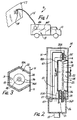
- FIG. 1 there is shown a liquid-jet plasma pinch surface treating system 9, which is constructed in accordance with the present invention, and which is adapted to be mounted on board of a mobile unit or vehicle 11 in the form of a vehicle such as a truck or van.
- the mobile unit 11 is able to transport conveniently the liquid-jet surface treating system 9 so that it can be utilized in a variety of applications such as applications involving large, bulky surfaces to be treated.
- the system 9 can be used to clean unwanted coating material from structures, including walls and other large surface areas.
- the system 9 can also be transported to an aircraft to strip its outer painted surface of its paints and the like, without polluting the air.
- the liquid-jet plasma pinch surface treating system 9 generally includes an on-board plasma control assembly or unit 13 connected via a cable 15 to an ultraviolet light emitting head or assembly 14 for treating a surface 17.
- the liquid-jet plasma pinch system 14 establishes a source of high intensity incoherent ultraviolet light radiation of a sufficiently high intensity that it will remove by sublimation, evaporation, photodecomposition and spallation unwanted coating material covering the surface 17.
- the short wavelength ultraviolet light radiated from the head 14 of the system 9 as illustrated by wavy lines penetrates the surface 17 to be treated, only to a very shallow depth, generally in the range of .1 ⁇ m or less. Accordingly, the radiated ultraviolet light will separate surface coatings (not shown) from its underlying substrates, without substantially affecting the underlying surface 17.
- a user drives the mobile unit 11 to a location near the surface 17.
- the user then manually or by means (not shown) positions the liquid-jet plasma pinch head 14 adjacent to the surface 17 to be stripped and activates the plasma control system 13.
- the liquid jet plasma pinch head 14 emits pulsed high intensity incoherent ultraviolet light which the user directs and guides along the surface of the object to be treated.
- the surface 17 of the object As the ultraviolet light bathes the surface 17 of the object, the surface is rapidly heated to cause the coating material to be separated from its substrate, and otherwise removed or discharged therefrom.
- a user of the system 9 can move the liquid-jet plasma pitch light emitting head 14 manually or by means (not shown) relative to the surface 17 to be treated.
- the surface 17 may form a part of a larger structure, such as an aircraft, building or any other such large object requiring surface treatment.
- the entire surface area of an item, such as an aircraft (not shown) may be treated with the high intensity incoherent ultraviolet light radiated by the liquid-jet plasma pinch system 9.
- the unit 13 includes a housing H, which has an inner elongated housing 18A having an evacuated sealed chamber 18, in which the liquid jet plasma pinch is established to produce the ultraviolet light.
- the liquid channel 16 extends axially within the chamber 18, and is initially in the form of a stream of liquid which flows under pressure through the chamber 18.
- a liquid vapor cloud 23 surrounds the liquid stream as it passes through the interior of the chamber 18, and cooperates therewith to form the main preionizing driver of the plasma system 12.
- the plasma control assembly 13 includes a pump 19 (FIG. 4) for maintaining the flow of liquid via the cable 15 through the chamber 18.
- the plasma control assembly 13 also includes a vacuum pump 20, which is connected in fluid communication via a suction or vacuum line 31 extending between the unit 13 and the head 14 via the cable 15, and for maintaining the chamber 18 evacuated.
- the plasma control system 13 also includes a liquid storage tank 21 which provides a source of liquid or fluid for the liquid-jet pinch head 14.
- a machine control computer 95 controls the operation of the plasma control system 13 and establishes the pulsing rate for an electrical discharge system 25 to cause the vapor cloud 23 to be ionized for producing the incoherent ultraviolet light emitted from liquid jet plasma head 14 as it traverses adjacent to the surface 17 to be treated.
- the discharge system 25 generates vapor ionizing high voltage pulses at a desired frequency, such as a frequency of between substantially one per second and substantially 1000 times per second, depending on the desired effect of the treatment.
- a more preferred range is between about 10 pulses per second and about 100 pulses per second.
- the most preferred repetition rate is about 100 pulses per second.
- the electrode assemblies 35 and 36 contain a liquid emitter 35A and a liquid receptor 36A respectively for directing the stream of liquid axially through the chamber 18.
- the discharge system 25 delivers the high voltage pulses across the assemblies 35 and 36, at a potential of approximately 30,000 volts, to cause an electrical current to flow initially through the vapor cloud 23 for plasma producing ionization purposes.
- the stream of liquid absorbs the energy emanating from the non-dense plasma or ionized vapor cloud 23, and is, in turn, heated thereby.
- the liquid stream then becomes ionized, and is transformed into a high-Z dense plasma pinch to provide the high intensity ultraviolet light.
- the generated plasma then conducts the continuing discharge electrical current, and produces high-intensity ultraviolet light.
- the generated dense pinched plasma diverts most of the discharge electrical current from the surrounding non-dense plasma, and conducts it along the channel 16 through the chamber 18.
- the resulting plasma is substantially stable, and substantially uniform in cross section throughout its length.
- liquid jet chamber housing 18 is generally an elongated vacuum chamber, which is polygonal in cross section throughout its axial length. In this regard, it is preferably generally hexagonal in cross section shape.
- a set of five reflective mirrors, such as a mirror 22 helps reflect or guide the incoherent ultraviolet light emitted from the high density plasma pinch through a transparent chamber window wall 24 forming a sixth wall through which the ultraviolet light is emitted toward the surface 17.
- the window wall 24 fits in, and is sealed over, by sealing means (no shown, an opening (not shown) in the wall "X" of the housing H.
- the transparent wall 24 is composed of material such as quartz, which is transparent to ultraviolet light.
- the liquid jet head 14 includes housing extension 26 having a pair of connectors 27 and 28 that permit fluid communication between the liquid storage system 21 and the electrode assemblies 35 and 36 inside the chamber 18.
- Connector 27 is an inlet connector for permitting liquid to flow under pressure via a conduit or tube 47 into the chamber 18, while connector 28 is an outlet connector for permitting liquid to flow from the chamber 18 back via a conduit or tube 36A into the liquid storage tank 29 located in mobile unit 11, the tubes 47 and 36A extending through the cable 15.
- the unit 13 includes a small extension housing 46 which is substantially similar to the corresponding extension housing 26, and which connects the end of the cable 15 to the unit 13.
- a control valve 37 disposed within the housing 60 controls the flow of liquid into the liquid storage tank 29.
- housing 60 confines the liquid storage tank 19, the vacuum pump 20, the discharge system 25, the machine control computer 95, and a portable power system (not shown) for supplying electrical power to the plasma control unit 13.
- the base housing unit 60 may include a set of rollers (not shown) so that it may be easily loaded onto and off of the mobile unit 11. In this manner, the entire system 9 can be transported by the mobile unit 11 to a remote location, and if desired, off loaded and moved to a locale not otherwise accessible to the mobile unit 11.
- an ultraviolet light surface treating system 509 which is also constructed in accordance with the present invention, and which is adapted for use in an inventive parts manufacturing process for treating the surface of a workpiece or object in the form of an engine block 520 having a cylinder bore 519 to be glazed.
- the illustrated and described system 509 is able to perform a variety of surface treating processes, such as biological decontamination, chemical decontamination, ceramic glazing, metal glazing, plastic film removal, metal film removal, and the like. It should therefore be understood that, although only a glazing process will hereinafter be described, the other mentioned processes, are performed in a similar substantially the same manner, with only the exposure time being varied to accomplish the intended purpose.
- the surface treating system 509 is similar to the liquid-jet plasma pinch system 9, except that the system 509 is adapted to treat inside surfaces, even on small parts.
- the system 509 includes a plasma source system 513 having a plasma pinch head 514, which emits a highly intense ultraviolet light, and which is adapted to be lowered into an opening, such as the bore 519.
- the ultraviolet light emitted from the plasma pinch head 514 is directed toward the interior surface of an object, such as the engine block cylinder 520.
- the engine block 520 and the head 514 are manually rotated relative to one another or by motive means (not shown) about the axis of the bore 519 so the entire interior wall surface of the cylinder bore 519 is exposed to the ultraviolet light emitted from the head 514, for glazing purposes.
- the plasma control unit 513 which is substantially identical to the plasma control assembly 13 of FIG. 1 flexible cable 515 which is similar to the cable 15 of FIG. 1, couples the plasma pinch head 514 to the control unit 513.
- a conveyor system positions the engine block 520 in the general proximity of the plasma pinch head 514.
- the plasma pinch head 514 is then manually positioned by means (not shown), entirely within the bore 519 adjacent to the surface 517 to be glazed.
- the plasma control assembly 513 is activated to cause the head 514 to emit high intensity incoherent ultraviolet light, which is directed radially against a portion of the cylindrical wall surface 517 to be glazed.
- the block 520 is then rotated manually or by means (not shown) about the axis of the device 514. Alternatively, the head can be rotated, and the block remains stationary.
- the interior wall surface 517 of the block 520 is rapidly heated to cause the surface to be glazed.
- the crane 710 is rollably supported on the ground 761 by wheels 762 and 763, and is able to transport the plasma pinch system 712 along the longitudinal axis of the ship 790 so that the entire exterior surface areas side of along either its longitudinal axis may be treated.
- the crane 710 supports from above a movable platform 711 for carrying the system 712 rollably on wheels such as wheels 764 and 765 aloud overhead tracks 764A and 765A of the crane 710, and for permitting the system 712 to be moved along the horizontal axis of the ship.
- the liquid jet plasma pinch system 712 is similar to the system 10 of FIG. 1 and establishes a source of high intensity incoherent ultraviolet light radiation of sufficient intensity to remove unwanted or undesired coating materials covering a surface of an object, such as the ship 790.
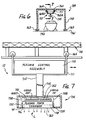
- the plasma pinch system 712 includes a plasma control assembly 713 which is mounted on the movable platform 711, and which is similar to the plasma control assembly of FIG. 1.
- the platform 711 is movable manually or by motive means (not shown).
- the system 712 also includes a liquid jet plasma pinch assembly or head 714 which is connected to the plasma control assembly 713 by a flexible cable 715, and which is similar to the head 14 of FIG. 1.
- the head 714 is also movable manually or by motive means (not shown) relative to the surface to be treated. In this manner, the entire surface area of a large object such as the ship 790, may be accomplished simply and conveniently.
- a user of the system may move the plasma pinch head 714 along the surface area of the object, to dislodge the unwanted and undesired coating materials.
- the head 714 generates a pulsed high intensity incoherent ultraviolet light, used to strip a coating from the surface of an object, such as the ship 790.
- the plasma is initiated within a liquid jet plasma pinch vacuum chamber assembly 718, which is similar to the chamber 18 of FIG. 1.
- a liquid jet is directed along the chamber axis as indicated in broken lines at 716, so as to form a plasma pinch in the region along the liquid jet, in a manner as previously for the head 14 of FIG. 2.
- the plasma control assembly 713 is connected via the depending flexible cable 715 to the head 714, and is similar to the control assembly 60 of FIG. 4.
- a pair of liquid conduits 751 and 752 conveying the plasma forming liquid under pressure into and out of the chamber 718.
- the discharge system (not shown) in the assembly 713 is connected via electrically leads 758 for generating high voltage electrical pulses to establish a plasma pinch along the liquid stream 716 thereamong.
- a pair of electrodes 730 and 732 are connected to the respective lines 758 and 758 for delivering plasma ionizing current along the liquid stream 716 between the electrodes 730 and 732.
- ultraviolet radiation L is emitted substantially uniformly over the duration of the pinch and is radiated through a window W.
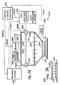
- FIG. 8 there is illustrated a semiconductor processing system 809, which is also constructed in accordance with the present invention; and which is adapted for use in a step of a semiconductor manufacturing process.
- the step of the process could be at an anneal, etching, super cleaning, or the like surface treatment of semiconductor materials, such as the semiconductor materials SM3, or 812 on a conveyor belt CB.
- the illustrated and described system 809 is a surface treating system, which is similar to the liquid jet plasma pinch surface treating system 9 described herein. While the system 809 is able to perform a variety of surface treating processes, such as super-cleaning semiconductor materials, annealing or etching of various components, chemical synthesis, and the like, a super-cleaning process will be described hereinafter in greater detail. However, it should be understood that the other mentioned processes are performed on substantially the same manner, with only the exposure time of the surface being varied to accomplish the intended process.
- system 809 is substantially similar to the liquid-jet plasma-pinch surface treating system 9 previously described, only those aspects of the system which are of significant difference will be described hereinafter in greater detail. It should be understood however, that the system 809 emits a highly intense pulsed ultraviolet light, which is directed toward the surface of an object, such as object 812 via an optical system generally indicated at 890.
- the optical system 890 permits a large amount of the incoherent radiated ultraviolet light to bathe the object 812 with a pulse highly intense ultraviolet light in an efficient manner, because of the light collecting and directing capabilities provided by the optical system 809.
- the system 809 utilizes a liquid-jet plasma-pinch system generally indicated at 810 for establishing a source of high intensity ultraviolet radiation indicated by the solid parallel lines indicated at R.
- the pinched plasma generates an ultraviolet light of sufficient intensity to super-clean the semiconductor material, such as material 812 or the material SM3, as they are being transported adjacent the optical lens system 890.
- the optical system 890 permits the radiated ultraviolet light to be reflected over the entire surface of the material.
- the liquid-jet plasma-pinch system 810 includes an enclosed processing chamber indicated at 818 for confining the liquid-jet plasma pinch 810 and the optical system 890.
- the processing chamber is in atmospheric communication with a source of inert gas, such as helium, which back-fills the chamber 818.
- the purpose of the inert gas is to help facilitate the passage of the emitted ultraviolet light in a generally unimpeded manner, known to those skilled in the art, that air or other non-inert gases react with and absorb the ultraviolet light thereby diminishing its life duration.
- the system 810 also includes a housing 818 defining a chamber with an outlet window or port, over which a pair of exposure doors 813 and 814 are movably manually, or by motive means (not shown) to be moved between a normally closed position over port P, and a fully opened position to expose the object or workpiece to the intense ultraviolet light emitted from the pinch system 810.
- Exposure doors 813 and 814 block the ultraviolet light emitted from the plasma pinch 840 from being exposed to a working area 816, until the next object, such as the semiconductor material SM3, is moved by the conveyor belt CB to the area 816 opposite the port.
- the liquid-jet plasma-pinch system 810 includes a plasma control assembly (not shown), which is substantially similar to plasma control assembly 13, and thus, will not be described hereinafter in greater detail.
- doors 813 and 814 are slidable mounted in a common vertical plane, and move toward and away from one another. When closed, they engage one another in a side-by-side configuration. When fully opened, they are spaced apart fully out of alignment with the port P.
- the optical system 890 generally includes a plurality of lenses, such as a spherical quartz lens 820, which individually fit within windows, such as a window 820A for the lens 820, of a plasma chamber shown diagrammatically at 832, within the larger chamber 819.
- the optical system 890 further includes a plurality of mirrors, such as mirror 830 disposed within chamber 819, outside chamber 832.
- the lenses focuses the high intensity incoherent ultraviolet light emitted radially from the plasma pinch, shown diagrammatically at 840 toward the mirrors, such as mirror 830 and from the mirrors forwardly to a common lens at the port P.
- the mirrors are so arranged to reflect light either directly or indirectly forwardly through the common lens 834 within the chamber 819, toward a single object surface such as the surface of the semiconductor material 812.
- a substantial portion of the high intensity incoherent ultraviolet light emitted from the plasma pinch 840 can be collected and directed toward the surface of the material to be treated.
- the lenses are arranged surrounding the plasma pinch 840 to focus the incoherent light from the pinch 840 radially outwardly from the inner plasma chamber 832.
- the forward or front lens 836 which focuses directly at the common lens 834, there is a corresponding mirror which reflects the light passing through the lens either directly to the common lens 834, or to another one of the mirrors and then to the common lens 834.
- the conveyor belt CB moves the material SM3 into the working area or exposure chamber 816 of the housing 818.
- the exposure doors 813 and 814 are moved manually or by motive means to their fully opened position, thereby permitting the material to be exposed to the ultraviolet light being focused within the working area 816 by the optical system 890.
- a temperature sensing or optical scattering device monitors the condition of the semiconductor material 812 so that the surface temperature will not be raised to an excess temperature that might either damage or modify the conductivity properties of the semiconductor material SM3.
- the exposure door 813 When the material has been raised to a sufficient temperature for super cleaning the surface thereof, the exposure door 813 is moved to a closed position to retain the helium therewithin, and the semiconductor material SM3 is carried via the conveyor belt CB out of the chamber. This process is repeated for each workpiece or material to be processed. It should be understood by the working area 816 being disposed within the chamber 818, working area 816 is also back filled with the inert helium gas to assure that a substantial portion of ultraviolet light generated by the plasma pinch 840 is able to be utilized in processing the semiconductor material SM3. As an alternative technique, the door can remain opened for a predetermined time interval so that the workpiece or object is exposed to the ultraviolet light for a predetermined time interval.
- the liquid-jet plasma-pinch system 810 may be mounted in a mobile unit (not shown) or in a fixed processing location, such as a processing center (not shown).
- the system 809 may be transported to a remote location to process a single work piece object or conversely, the system 809 may be set up in a manufacturing facility to process a multiple number of work piece objects on an assembly line basis.
- FIG. 1A there is illustrated a semiconductor processing system 10A, which is prior art, and which is adapted for use in a semiconductor manufacturing process, for annealing semiconductor material, such as the material W.
- semiconductor processing system 10A Before considering the inventive semiconductor processing system, it is well to review the prior art system 10A to better understand the short comings of the prior known techniques.
- the system 10A is described briefly, as being illustrative of prior known excimer laser annealing techniques.
- the system 10A includes an excimer laser 12A, which emits a laser beam B directed toward the semiconductor material W and rapidly scanned across the surface thereof.
- the scanning rate of the laser beam B, as it traverses across the surface of the semiconductor material, is controlled so that the heat generated by the beam, causes the uniform activation of a dopant (not shown) implanted therewithin for annealing purposes.
- the excimer laser device 12A is conventional and may be a laser, such as the one marketed by Cymer Laser, Inc. of San Diego, California, for generating the laser beam, which is generally illustrated as a line designated as B.
- the laser beam B is directed by the excimer laser 12A toward a laser beam scanning system generally indicated at 14A, which redirects the laser beam directly transversely toward the surface of the semiconductor material W for annealing it.
- the excimer laser system 10A includes a machine control computer 16A, such as the one marketed by Allen Bradley Company, to control the operation of the system 10A.
- a temperature sensor 18A supplies a signal indicative of the temperature of the surface of the material W being annealed, via a lead 17A.
- a beam scanner 27A controlled by the computer 16A via a lead 19A carries a lens 25A to move the beam B scanningly.
- the excimer laser 12A emits the laser beam B toward the laser beam scanning system 14A, under the control of the machine control computer 16A for directing the laser beam B scanningly across the surface of the semiconductor material W in a predetermined X-Y pattern to cover it uniformly.
- the surface of the semiconductor material is annealed by heating it in a very rapid manner.
- the temperature sensor 18A For the purpose of optimizing the annealing of the surface of the semiconductor material W, the temperature sensor 18A, such as an infrared temperature sensor, sends a surface temperature indicative signal to the machine control computer 16A, to monitor the process. Upon receipt of this signal, the machine control computer 16A modulates the laser power or scan rate to maintain optimum processing.
- the beam B causes the temperature of the material W to rise in a rapid manner to the predetermined annealing temperature and the sensor causes the computer to control the process parameters for optimum performance.
- the machine control computer 16A is programmed to cause the laser beam scanning system 14A to direct the laser beam B, generated by the excimer laser device 12A, in a predetermined pattern toward the semiconductor material W through a window 14AA transparent to the beam B. It should, therefore, be understood that the machine control computer 16A is programmed in a conventional manner, to cause the laser beam B to be scanned at a controlled rate in a precise pattern and thus to cause the unwanted and undesirable overlapping of the beam scanning pattern, to achieve non-uniform dopant activation.
- the laser beam scanning system 14A includes a pair of mirrors, such as mirrors 21A and 23A which direct the laser beam B from the laser 12A toward the lens 25A interposed between the mirror 23A and the window 14AA, through which is directed the beam B onto the surface of the semiconductor material W.
- the beam scanner 27A is conventional, and may be a scanner manufactured by A & R Industries of Oceanside, California.
- the scanner 27A causes the lens 25A to deflect the laser beam B in a desired direction scanningly toward the surface of the semiconductor material.
- the beam scanner 27A is responsive to its control signal received from the computer via the lead 19A.
- the excimer laser 12A, the computer 16A, and the beam scanner 27A are extremely expensive equipment. Furthermore, the excimer laser is highly inefficient, and the system 10A would have an unsatisfactorily low throughput in actual production processes.
- FIG. 2A there is illustrated a semiconductor processing system 209A, which is adapted for use in a semiconductor manufacturing process for circuitizing the surface of semiconductor material, such as material SM1.
- the illustrated and described system is able to perform an etching process, employing a series of conventional etching masks, such as a mask M, having a desired circuit configuration (not shown) thereon and between the system 209A and the semiconductor material SM1.
- the system 209A emits light L which is directed toward the semiconductor material SM1 and the mask M interposed between the system 209A and individual ones of the semiconductor material SM1, for serving as a portion of a manufacturing process for semiconductor chips.
- the surface of the material becomes etched in a pattern determined by the mask M.
- the remaining portions of the etching process are conventional and are not described herein.
- the system 209A generally utilizes a gas embedded plasma pinch to generate ultraviolet light L used to etch the material SM1.
- the plasma is initiated by lasing activity taking place within a vacuum chamber 212A containing a gas, such as Argon.
- the system 209A includes a lasing system 214A for establishing along a chamber axis 216A of the chamber 212A a plasma pinch by exciting gas within a limited volume of the chamber 212A.
- a discharge system 218A ionizes the gas along the chamber axis as indicated at 216A so as to form a plasma pinch in the region preconditioned by the laser beam.
- a heat exchange unit 270A and a blower 280A cool and circulate the spent pinch gas of the system 209A as it is repetitively activated during the inventive process.
- the firings of the preconditioning and discharge system 214A and 218A are controlled by a machine control computer 285A via leads 285BA and 285AA respectively.
- An IR temperature sensing unit 286A detects the post-pulse residual temperature rise of the surface of the material SM1 being processed, and sends an electrical signal indicative of the processing performance to the computer 285A, via lead 285CA.
- the blower unit 280A is, in turn, controlled by the computer 285A via lead 285DA.
- the computer 285A can increase or decrease the intensity of the firings of the discharge system 218A in a precise manner.
- the lasing system 214A is well known and completely described in greater detail in U.S. patent 4,450,568.
- gas is injected into the chamber 216A.
- the preconditioning system 214A via a low power laser beam generator 242A supplies a preconditioning beam which is transmitted into the chamber 212A through a preconditioning beam window 238A and along the chamber axis 236A.
- the preconditioning beam excites the gas particles in the vicinity of the chamber axis 236A, thus defining the preconditioned channel within which the plasma pinch is then formed.
- the discharge system 218A is connected to the preconditioning system 214A via line 218AA to coordinate its actuation and for generating an intense electrical pulse along the chamber axis or channel 216A to establish a plasma pinch therealong.
- the discharge system is coupled to a pair of electrodes 230A and 232A via lines 258AA and 258BA for delivering current between the electrodes 230A and 232A.
- the discharge system 218A delivers a stored charge between the electrodes 230A and 232A along the channel 216A inasmuch as it is composed of excited gas particles and thus conductive relative to the unexcited particles surrounding the channel.
- the current ionizes particles within the channel 216A to establish a plasma and to create a circumferential magnetic field.
- the magnetic field interacts with the current creating a centripetal force on the plasma tending to constrict or pinch the plasma toward and along the chamber axis 216A.
- vacuum ultraviolet radiation is emitted substantially uniformly over the duration of the pinch.
- the vacuum ultraviolet radiation released by the pinch radiates throughout the chamber and is reflected by the mirror 228A and downwardly through a bottom transparent chamber wall 260A, and outwardly through the mask M, and from there, through a lens 290A and onto the top surface of the semiconductor material SM1 for etching purposes.
- the machine control computer 285A controls and coordinates the operation of discharge system 218A, so that the system 209A may be repetitively activated at a very high rate of speed.
- the temperature sensor 286A senses the post-pulse surface temperature rise of the semiconductor material.
- the temperature sensor 286A sends a signal to the machine control computer 285A indicative of the surface treatment level.
- the machine control computer 285A responds to this signal and causes the system 209A to be repetitively activated at a predetermined rate, until the entire wafer has been covered. It is in this manner that the processing of the semiconductor material SM1 may be precisely controlled for the etching process.
- the ultraviolet radiation released by the plasma pinch is radiated through the lens 290A, the light is radiated on the mask M which includes a predetermined circuit pattern.
- the mask M thus allows only certain portions of the ultraviolet radiation to reach the surface of the semiconductor material SM1. It is this portion of the radiated ultraviolet light which etches the surface of the semiconductor material.
- the system 209A operates at a very fast repetition rate, in that it produces light pulses at a duration of about one millionth of a second.
- the repetition rate of the UV light pulses can be adjusted under the control of the computer 285A, between about 1 pulse per second, and about 1,000 pulses per second. A more preferred range is between about 10 pulses per second and about 100 pulses per second. The most preferred repetition rate is about 100 pulses per second.
- FIG. 3A there is illustrated a semiconductor processing system 309A, which is constructed in accordance with the present invention; and which is adapted for use in an inventive semiconductor manufacturing process for annealing the surface of semiconductor material, such as semiconductor material SM2.
- the illustrated and described system 309A is an annealing system, which is similar to the semiconductor etching system 209A described herein.
- the system 309A includes a lasing system (not shown) having a vacuum chamber 312A and an optical system 390A.
- the optical system 390A permits the radiated ultraviolet light to bathe the entire upper surface area of the semiconductor material SM2.
- the system 309A is similar to the system 209A, except for the absence of the etching mask M.
- a single burst of the ultraviolet light causes the surface temperature of the semiconductor material SM2 to be raised. This rise in surface temperature is sensed by a temperature sensor (not shown), which sends a signal to a machine control computer (not shown) indicative of the surface temperature of the material SM2.
- the machine control computer in response to this signal causes the lasing system (not shown) to be repetitively fired, until the entire surface or set of wafers have been covered. Thereafter, the machine control computer terminates the firing operation so a new piece of semiconductor material may be processed in a similar manner.
- FIG. 4A there is illustrated a semiconductor processing system 409A, which is also constructed in accordance with the present invention; and which is adapted for use in an inventive semiconductor manufacturing process for annealing the surface of semiconductor material, such as material SM3.
- the system 409A emits a highly intense ultraviolet light which is directed toward the semiconductor material SM3 via an optical system 490A.
- the optical system 490A permits the radiated ultraviolet light to bathe the semiconductor material SM3A.
- the system 409A generally utilizes a liquid jet plasma pinch system 410A for establishing a source of high intensity ultraviolet radiation.
- the liquid jet plasma pinch system 410A includes a plasma source liquid-jet pinch device or apparatus 412A, to establish a central narrow preconditioned liquid channel which is generally illustrated in broken line at 414A, for the plasma to be formed and pinched therealong, within a limited volume of a closed chamber 416A.
- the liquid channel 414A is initially in the form of a stream of liquid which flows under pressure through the chamber 416A maintained evacuated by means of a vacuum pump 461A.
- a vapor cloud 423A surrounds the liquid stream, and cooperates therewith to form the main preionizing driver of the plasma system 410A.
- An electrical discharge system 425A is coupled to a pair of axially spaced apart electrode assemblies 435A and 436A at opposite ends of the chamber 416A, for directing the stream of liquid through the chamber 416A and for establishing an electrical current flow through the preconditioning vapor cloud 423A of liquid along channel 414A to establish the plasma.
- a machine control computer 495A establishes the repetition rate at which the liquid jet plasma pinch system 410A is fired. This rate is the same as that described in connection with the system 209A. Also, the pulse width is the same as described in connection with the system 209A.
- the machine control computer 495A is coupled between a temperature sensor 496A via a lead 494A and the discharge system 425A via a lead 498A.
- the machine control computer 495A is also connected to a vacuum pump 461A for the purpose of controlling the evacuation of the vacuum chamber 416A after each firing.
- the computer 495A is also connected to a source of liquid 446A under pressure via the lead 498A.
- the machine control computer 495A is also connected to a motor 497A for driving a conveyor belt system shown generally at 497A.
- the conveyor belt system 497A transports the individual ones of the semiconductor material under the lens system 490A, to be irradiated by the ultraviolet light emitted therefrom.
- a fine stream of liquid flows under pressure axially between the electrode assemblies 435A and 436A inside the chamber 416A.
- the discharge system 425A is thereafter activated for delivering a high voltage potential, such as approximately 30,000 volts, across the electrodes 435A and 436A, to cause an electrical current to flow initially through the vapor cloud 423A.
- the stream absorbs the energy emanating from the non-dense plasma or ionized vapor cloud 423A, and is, in turn, heated thereby.
- the liquid stream then becomes ionized, and is transformed into a high-Z dense plasma pinch.
- the generated plasma then conducts the continuing discharge electrical current, and produces high-intensity ultraviolet light.
- the generated dense pinched plasma diverts most of the discharge electrical current from the surrounding non-dense plasma, and conducts it along the channel 414A through the chamber 416A.
- the resulting plasma is substantially stable, and is substantially uniform in cross section throughout its length.
- the pinched plasma generates an ultraviolet light of sufficient intensity to anneal the semiconductor material, such as materials SM3, SM4 and SM5 as they are transported under the lens system 490A.
- the semiconductor material is of different sizes, and the optical system 490A permits the radiated ultraviolet light to be reflected over the entire surface of the material, regardless of its size.
- the computer 495A can control the system 490A via a control lead 501A.
- the plasma becomes extinguished and then is re-established repeatedly by the activation of the device 425A under the control of the machine control computer 495A.
- the foregoing steps of the process are repeated each time for re-establishing the plasma pinch in a recurring manner.
- the remote temperature sensing device 496A senses the surface temperature of the semiconductor material SM3. As it is heated by the radiated ultraviolet light, the remote temperature sensing unit 496A sends a signal to the machine control computer 495A to indicate that proper treatment has been achieved.
- the computer 495A upon receipt of this signal, causes the repetitively pulsated ultraviolet light to be supplied to the wafer until a desired surface area is covered. Once the entire surface or set of wafers has been covered, the pulsing action is terminated under the control of the machine control computer 495A.
- the surface of the semiconductor material is processed to form a semiconductor device with a shallow junction having minimal dopant diffusion.
Landscapes
- Physics & Mathematics (AREA)
- Engineering & Computer Science (AREA)
- Plasma & Fusion (AREA)
- Chemical & Material Sciences (AREA)
- Spectroscopy & Molecular Physics (AREA)
- Optics & Photonics (AREA)
- Nanotechnology (AREA)
- Crystallography & Structural Chemistry (AREA)
- Mathematical Physics (AREA)
- General Physics & Mathematics (AREA)
- Theoretical Computer Science (AREA)
- Physical Or Chemical Processes And Apparatus (AREA)
- Forging (AREA)
- Cleaning In General (AREA)
- Weting (AREA)
- Cleaning Or Drying Semiconductors (AREA)
- Cleaning And De-Greasing Of Metallic Materials By Chemical Methods (AREA)
- Threshing Machine Elements (AREA)
Claims (25)
- Verfahren zum Behandeln einer Oberfläche (17) umfassend:
Verwenden eines beabstandeten Paares aus einer Kombinations-Flüssigkeitsemitter-(35A) und -Elektrodeneinrichtung (35) und einer Kombinations-Flüssigkeitsrezeptor- (36A) und -Elektrodeneinrichtung (36);
Strömenlassen eines feinen Flüssigkeitsstroms (16) zwischen dem Paar von Elektrodeneinrichtungen (35, 36) mit einem ausreichenden Druck in einer ziemlich schmalen, geradlinigen und fokussierten Konfiguration, um die Ausbildung einer dünnen vorkonditionierenden Flüssigkeitsdampfwolke (23) zu veranlassen, die den fließenden feinen Flüssigkeitsstrom umgibt;
Einrichten einer elektrischen Spannungspotentialdifferenz zwischen der Elektrodeneinrichtung mit einer ausreichend hohen Spannung, um einen elektrischen Strom dazu zu bringen, durch die Flüssigkeitsdampfwolke zu fließen, um zunächst dort ein Plasma geringer Dichte zu erzeugen, welches ausreicht, daß Energie von ihm in den fließenden Flüssigkeitsstrom gelangt und diesen ausreichend erhitzt, so daß er ansprechend auf das Plasma geringer Dichte ionisiert und in ein Plasma hoher Dichte umgewandelt wird;
Verwenden einer Plasmaeinschnüranordnung (14), die über ein Kabel (15) mit einer Plasmasteueranordnung (13) gekoppelt ist, wobei die Kombinations-Flüssigkeitsemitter- und -Elektrodeneinrichtung und die Kombinations-Flüssigkeitsrezeptor- und -Elektrodeneinrichtung im Inneren der Plasmaeinschnüranordnung gelagert sind und mit der Plasmasteueranordnung gekoppelt sind;
Bewegen der Steueranordnung in die Nähe der zu behandelnden Oberfläche; und
Bewegen der Plasmaeinschnüranordnung relativ zu der zu behandelnden Oberfläche, um die Oberfläche hochintensiven, nicht-kohärentem Ultraviolettlicht auszusetzen, welches aus dem hochdichten Plasma abstrahlt. - Verfahren nach Anspruch 1, bei dem das Behandeln Glassieren ist und die Oberfläche eine Oberfläche aus der Gruppe Metall und Keramiken ausgewählt ist.
- Verfahren nach Anspruch 1, bei dem die Behandlung Reinigen ist, um Substanzen von der Oberfläche zu lösen.
- Verfahren nach Anspruch 1, bei dem die Behandlung ein Markieren der Oberfläche ist.
- Vorrichtung zum Behandeln einer Oberfläche (17) umfassend:
ein beabstandetes Paar aus einer Kombinations-Flüssigkeitsemitter- (35A) und -Elektrodeneinrichtung (35) und einer Kombinations-Flüssigkeitsrezeptor- (36A) und -Elektrodeneinrichtung (36);
eine Einrichtung zum Erzeugen eines feinen Flüssigkeitsstroms (16) zwischen dem Paar von Elektrodeneinrichtungen bei ausreichendem Druck in einer ziemlich schmalen, geradlinigen und fokussierten Konfiguration, um die Ausbildung einer dünnen vorkonditionierenden Flüssigkeitsdampfwolke (23) zu veranlassen, die den feinen Flüssigkeitsstrom umgibt;
eine Entladungseinrichtung zum Erzeugen einer elektrischen Spannungspotentialdifferenz zwischen den Elektrodeneinrichtungen mit ausreichend hoher Spannung, um zu veranlassen, daß ein elektrischer Strom durch die Flüssigkeitsdampfwolke fließt, so daß dort herum zu Beginn ein Plasma geringer Dichte entsteht, ausreichend, damit Energie aus ihm heraus in den Flüssigkeitsstrom gelangt, um diesen so stark zu erhitzen, daß er ionisiert und ansprechend auf das Plasma geringer Dichte in ein Plasma hoher Dichte umgewandelt wird;
eine Plasmaeinschnüranordnung (14) zum Aufnehmen des Plasmas hoher Dichte, wobei die Plasmaeinschnüranordnung eine Vakuumkammereinrichtung (18) aufweist zum Begrenzen des Plasmas, wobei die Kombinations-Flüssigkeitsemitter- und -Elektrodeneinrichtung und die Kombinations-Flüssigkeitsrezeptor- und Elektrodeneinrichtung im Inneren der Vakuumkammereinrichtung gelagert sind;
eine Plasmasteueranordnung (13) zum Liefern der elektrischen Spannung und der Flüssigkeit an die Plasmaeinschnüranordnung;
ein flexibles Kabel (15) zum Koppeln der Plasmasteueranordnung mit der Plasmaeinschnüranordnung;
eine Einrichtung zum Lagern der Plasmaeinschnüranordnung relativ zu der Plasmasteueranordnung; und
eine Einrichtung zum beweglichen Aufnahmen der Plasmasteueranordnung relativ zu der zu behandelnden Oberfläche. - Vorrichtung nach Anspruch 5, bei der die Kombinations-Flüssigkeitsemitter-Elektrodeneinrichtung und Kombinations-Flüssigkeitsrezeptor- und -Elektrodeneinrichtung jeweils aufweisen:
ein Innenrohr aus einem elektrisch leitenden Material, so daß elektrischer Strom hindurchfließen kann;
eine in Fluidverbindung mit dem Innenrohr stehende Einrichtung zum Ermöglichen einer Flüssigkeitsverbindung zwischen dem Innenrohr und dem Flüssigkeitsstrom; und
ein Außenrohrelement mit einer Düseneinrichtung, die in Fluidverbindung mit dem Rohr steht. - Vorrichtung nach Anspruch 5, umfassend eine Einrichtung zum Drehen der Plasmaeinschnüranordnung (514).
- Vorrichtung (809) zum Behandeln der Oberfläche eines Objekts (812) umfassend:
eine Plasmaeinschnüreinrichtung (810) zum Schaffen einer Quelle für inkohärentes Ultraviolettlicht ausreichender Stärke zum Behandeln der Oberfläche, einschließlich einer Plasmakammereinrichtung (832) zum Eingrenzen des Plasmas;
eine optische Einrichtung (890) zum Leiten des von der Plasmaeinschnüreinrichtung (810) erzeugten inkohärenten Ultraviolettlichts in Richtung auf die zu behandelnde Oberfläche;
eine Einrichtung zum Belichten des Objekts (812) mit dem von der optischen Einrichtung (890) kommenden inkohärenten Ultraviolettlicht; und
eine Gaskammereinrichtung (818) zum Eingrenzen der Plasmakammereinrichtung (832) und des Objekts (812). - Vorrichtung nach Anspruch 8, bei der die optische Einrichtung mehrere Elemente aufweist, die die Plasmaeinschnüranordnung (840) derart umgebend angeordnet sind, daß sie das von ihr kommende Licht durch ein Auslaßport (P) in der Gaskammereinrichtung lenken.
- Vorrichtung nach Anspruch 9, bei der die Elemente Linsen (820, 834, 836) und reflektierende Glieder (830) enthalten.
- Vorrichtung nach Anspruch 8, bei der die Einrichtung zum Belichten des Objekts (812) mit dem inkohärenten Ultraviolettlicht eine Einrichtung (813, 814) aufweist, um das Objekt (812) eine vorbestimmte Zeitspanne zu exponieren.
- Vorrichtung nach Anspruch 8, bei der die Gaskammereinrichtung (818) außerdem die optische Einrichtung (890) einschließt.
- Vorrichtung nach Anspruch 8, bei der ein inertes Gas sich im Inneren der Gaskammereinrichtung (818) befindet.
- Verfahren zum Behandeln einer Oberfläche eines Objekts (805), umfassend:
Verwenden einer Plasmaeinschnüreinrichtung (810) zum Schaffen einer Quelle für inkohärentes Ultraviolettlicht;
Verwenden einer optischen Einrichtung, um das inkohärente Ultraviolettlicht auf das Objekt (812) zu richten;
Verwenden einer Einrichtung zum Belichten des Objekts (812) mit dem inkohärenten Ultraviolettlicht von der optischen Einrichtung (890);
Eingrenzen der Plasmakammereinrichtung (832) und des Objekts (812) in einer Gaskammereinrichtung (818). - Verfahren nach Anspruch 14, bei dem das Verwenden der Einrichtung zum Belichten des Objekts (812) mit dem inkohärenten Ultraviolettlicht das Bewegen des Objekts (810) im Inneren der Gaskammereinrichtung (818) beinhaltet.
- Verfahren nach Anspruch 14, bei dem das Verwenden der Einrichtung zum Belichten des Objekts (812) mit dem inkohärenten Ultraviolettlicht das Belichten des Objekts (812) für eine vorbestimmte Zeitspanne beinhaltet.
- Verfahren nach Anspruch 14, gekennzeichnet durch das Eingrenzen der optischen Einrichtung (890) im Inneren der Gaskammereinrichtung.
- Verfahren nach Anspruch 14, weiterhin umfassend das Einbringen von inertem Gas in die Gaskammereinrichtung (818), um die Verringerung der Impedanz gegenüber dem Durchlauf des inkohärenten ultravioletten Lichts durch sie hindurch zu unterstützen.
- Verfahren zum Behandeln der Oberfläche eines Halbleitermaterials (819), um dessen Leitungseigenschaften zu variieren, umfassend:
Verwenden einer Plasmaeinschnüreinrichtung zum Bilden von inkohärentem Ultraviolettlicht ausreichender Stärke, damit die Leitungseigenschaften praktisch der gesamten ebenen Oberfläche des Halbleitermaterials gleichmäßig variiert werden, wobei das Bilden die Verwendung eines beabstandeten Paares aus einer Kombinations-Flüssigkeitsemitter- (35A) und -Elektrodeneinrichtung (35) und einer Kombinations-Flüssigkeitsrezeptor- (36A) und -Elektrodeneinrichtung (36) umfaßt sowie das Ausbilden eines feinen Flüssigkeitsstroms zwischen dem Paar von Elektrodeneinrichtungen (35, 36) mit ausreichendem Druck in einer ziemlich schmalen, geradlinigen und fokussierten Konfiguration, damit sich dort herum eine dünne vorkonditionierende Flüssigkeitsdampfwolke (23) ausbildet, die den feinen Flüssigkeitsstrom unter Druck umgibt;
Bilden einer elektrischen Spannungspotentialdifferenz zwischen den Elektrodeneinrichtungen (35, 36) mit einer ausreichend hohen Spannung, um einen elektrischen Stromfluß durch die Flüssigkeitsdampfwolke (23) zu veranlassen und damit die anfängliche Erzeugung von Plasma geringer Dichte entlang der Wolke, ausreichend, um aus ihm Energie in den Flüssigkeitsstrom gelangen zu lassen, damit er ausreichend erhitzt wird, um ionisiert und ansprechend auf das Plasma geringer Dichte in ein Plasma hoher Dichte umgewandelt zu werden und so hochintensives inkohärentes Ultraviolettlicht zu erzeugen;
Richten des Ultraviolettlichts auf die gesamte Oberfläche des Halbleitermaterials (812), welches aus einem Halbleitermaterial besteht, das einen implantierten Dotierstoff für die Erhitzung über die gesamte Oberfläche aufweist;
wiederholtes Pulsieren des Ultraviolettlichts mit einer Geschwindigkeit von mindestens einmal pro Sekunde, um die Leitungseigenschaften des gesamten Halbleitermaterials ansprechend darauf zu variieren; und
Beendigen des Erhitzens der behandelten Halbleiteroberfläche. - Verfahren nach Anspruch 19, bei dem die Oberfläche des Halbleiters soweit erhitzt wird, daß die Aktivierung des implantierten Dotierstoffs zur Bildung eines Halbleiters veranlaßt wird, der einen flachen Übergang von weniger als 0,1 mm besitzt.
- Verfahren nach Anspruch 19 oder 20, weiterhin umfassend:
Verwenden einer Temperaturmeßeinrichtung;
kontinuierliches Messen der Oberflächentemperatur des Halbleitermaterials, wenn dies dem pulsierenden Ultraviolettlicht ausgesetzt wird; und
Beenden des Erhitzens der behandelten Halbleiteroberfläche dann, wenn der Oberflächenbereich vollständig abgedeckt wurde. - Verfahren nach Anspruch 21, bei dem das Erhitzen der Oberfläche des behandelten Halbleitermaterials dann abgeschlossen wird, wenn die Oberflächentemperatur des Halbleiters auf eine Temperatur von 800°C bis 1200°C erwärmt wurde.
- Verfahren nach Anspruch 21, bei dem das Erwärmen der Oberfläche des behandelten Halbleitermaterials dann beendet wird, wenn die Oberflächentemperatur des Halbleiters auf einer Temperatur von 1050°C erwärmt ist.
- Verfahren nach Anspruch 19, bei dem das Ultraviolettlicht mit einer Geschwindigkeit von zwischen einmal pro Sekunde und 1000-mal pro Sekunde gepulst wird.
- Verfahren nach Anspruch 19, bei dem das Ultraviolettlicht mit einer Geschwindigkeit zwischen einmal pro Sekunde und 10-mal pro Sekunde pulsiert wird.
Applications Claiming Priority (5)
| Application Number | Priority Date | Filing Date | Title |
|---|---|---|---|
| US07/347,422 US5079187A (en) | 1987-12-07 | 1989-05-04 | Method for processing semiconductor materials |
| US347422 | 1989-05-05 | ||
| US07/425,865 US5204506A (en) | 1987-12-07 | 1989-10-24 | Plasma pinch surface treating apparatus and method of using same |
| US425865 | 1989-10-24 | ||
| PCT/US1990/002480 WO1990013910A1 (en) | 1989-05-04 | 1990-05-04 | Method and apparatus for processing materials |
Publications (3)
| Publication Number | Publication Date |
|---|---|
| EP0441905A1 EP0441905A1 (de) | 1991-08-21 |
| EP0441905A4 EP0441905A4 (en) | 1991-12-18 |
| EP0441905B1 true EP0441905B1 (de) | 1995-09-06 |
Family
ID=26995261
Family Applications (1)
| Application Number | Title | Priority Date | Filing Date |
|---|---|---|---|
| EP90908390A Expired - Lifetime EP0441905B1 (de) | 1989-05-04 | 1990-05-04 | Vorrichtung und verfahren zur behandlung von materialien |
Country Status (5)
| Country | Link |
|---|---|
| EP (1) | EP0441905B1 (de) |
| AT (1) | ATE127651T1 (de) |
| AU (1) | AU5725690A (de) |
| DE (1) | DE69022212D1 (de) |
| WO (1) | WO1990013910A1 (de) |
Families Citing this family (5)
| Publication number | Priority date | Publication date | Assignee | Title |
|---|---|---|---|---|
| US7025831B1 (en) | 1995-12-21 | 2006-04-11 | Fsi International, Inc. | Apparatus for surface conditioning |
| US6465374B1 (en) | 1997-10-21 | 2002-10-15 | Fsi International, Inc. | Method of surface preparation |
| US6165273A (en) | 1997-10-21 | 2000-12-26 | Fsi International Inc. | Equipment for UV wafer heating and photochemistry |
| CN1155990C (zh) * | 1998-11-16 | 2004-06-30 | Fsi国际股份有限公司 | Uv基片加热和光化学的设备 |
| US10415552B2 (en) | 2017-02-07 | 2019-09-17 | The Boeing Company | Injection system and method for injecting a cylindrical array of liquid jets |
Family Cites Families (10)
| Publication number | Priority date | Publication date | Assignee | Title |
|---|---|---|---|---|
| US3946332A (en) * | 1974-06-13 | 1976-03-23 | Samis Michael A | High power density continuous wave plasma glow jet laser system |
| US4369514A (en) * | 1980-10-30 | 1983-01-18 | Bell Telephone Laboratories, Incorporated | Recombination laser |
| US4450568A (en) * | 1981-11-13 | 1984-05-22 | Maxwell Laboratories, Inc. | Pumping a photolytic laser utilizing a plasma pinch |
| US4454835A (en) * | 1982-09-13 | 1984-06-19 | The United States Of America As Represented By The Secretary Of The Navy | Internal photolysis reactor |
| JPS59129772A (ja) * | 1983-01-18 | 1984-07-26 | Ushio Inc | 光化学蒸着装置 |
| US4522657A (en) * | 1983-10-20 | 1985-06-11 | Westinghouse Electric Corp. | Low temperature process for annealing shallow implanted N+/P junctions |
| JPS60175351A (ja) * | 1984-02-14 | 1985-09-09 | Nippon Telegr & Teleph Corp <Ntt> | X線発生装置およびx線露光法 |
| US4624736A (en) * | 1984-07-24 | 1986-11-25 | The United States Of America As Represented By The United States Department Of Energy | Laser/plasma chemical processing of substrates |
| US4718974A (en) * | 1987-01-09 | 1988-01-12 | Ultraphase Equipment, Inc. | Photoresist stripping apparatus using microwave pumped ultraviolet lamp |
| US4889605A (en) * | 1987-12-07 | 1989-12-26 | The Regents Of The University Of California | Plasma pinch system |
-
1990
- 1990-05-04 WO PCT/US1990/002480 patent/WO1990013910A1/en not_active Ceased
- 1990-05-04 AU AU57256/90A patent/AU5725690A/en not_active Abandoned
- 1990-05-04 EP EP90908390A patent/EP0441905B1/de not_active Expired - Lifetime
- 1990-05-04 DE DE69022212T patent/DE69022212D1/de not_active Expired - Lifetime
- 1990-05-04 AT AT90908390T patent/ATE127651T1/de not_active IP Right Cessation
Also Published As
| Publication number | Publication date |
|---|---|
| DE69022212D1 (de) | 1995-10-12 |
| EP0441905A1 (de) | 1991-08-21 |
| EP0441905A4 (en) | 1991-12-18 |
| WO1990013910A1 (en) | 1990-11-15 |
| AU5725690A (en) | 1990-11-29 |
| ATE127651T1 (de) | 1995-09-15 |
Similar Documents
| Publication | Publication Date | Title |
|---|---|---|
| KR100189794B1 (ko) | 피처리물의 산화방법 | |
| US12160936B2 (en) | Heat treatment apparatus of light irradiation type and method for cleaning heat treatment apparatus | |
| US5204506A (en) | Plasma pinch surface treating apparatus and method of using same | |
| US5174826A (en) | Laser-assisted chemical vapor deposition | |
| US6291796B1 (en) | Apparatus for CFC-free laser surface cleaning | |
| EP0693978A1 (de) | Gutfernung von oberflächen-verseuchungen durch ausstrahlung | |
| US6627846B1 (en) | Laser-driven cleaning using reactive gases | |
| EP0633823B1 (de) | Entfernung von oberflächen-verseuchungen durch ausstrahlung | |
| KR20210115058A (ko) | 챔버 부품들을 제조하기 위한 방법 | |
| US5048163A (en) | System for processing semiconductor materials | |
| JP2001232317A (ja) | 基体の表面を処理するための方法および装置 | |
| WO1990013910A1 (en) | Method and apparatus for processing materials | |
| CN1043846A (zh) | 等离子体收缩系统及其使用方法 | |
| US5079187A (en) | Method for processing semiconductor materials | |
| JP2007007644A (ja) | ディスプレイ製造におけるシャドウマスクの洗浄方法(変形)および装置 | |
| JP2002079077A (ja) | 処理装置および処理方法 | |
| JP2579346Y2 (ja) | レジスト膜のアッシング装置 | |
| JP2702697B2 (ja) | 処理装置および処理方法 | |
| CN111149064A (zh) | 处理头、处理系统以及处理基板的局部表面区域的方法 | |
| RU2024367C1 (ru) | Способ электроэрозионной обработки диэлектриков | |
| KR100540519B1 (ko) | 처리 장치 및 처리 방법 | |
| RU2002339C1 (ru) | Способ плазменной обработки поверхности твердого тела струей газообразного теплоносител | |
| JPH01103840A (ja) | ドライエツチング方法 | |
| JPH1150274A (ja) | 切断加工方法および装置 | |
| JP2002151440A (ja) | ウェーハダイシング方法及びその装置 |
Legal Events
| Date | Code | Title | Description |
|---|---|---|---|
| PUAI | Public reference made under article 153(3) epc to a published international application that has entered the european phase |
Free format text: ORIGINAL CODE: 0009012 |
|
| 17P | Request for examination filed |
Effective date: 19910513 |
|
| AK | Designated contracting states |
Kind code of ref document: A1 Designated state(s): AT BE CH DE DK ES FR GB IT LI LU NL SE |
|
| A4 | Supplementary search report drawn up and despatched |
Effective date: 19911029 |
|
| AK | Designated contracting states |
Kind code of ref document: A4 Designated state(s): AT BE CH DE DK ES FR GB IT LI LU NL SE |
|
| 17Q | First examination report despatched |
Effective date: 19940114 |
|
| GRAA | (expected) grant |
Free format text: ORIGINAL CODE: 0009210 |
|
| AK | Designated contracting states |
Kind code of ref document: B1 Designated state(s): AT BE CH DE DK ES FR GB IT LI LU NL SE |
|
| PG25 | Lapsed in a contracting state [announced via postgrant information from national office to epo] |
Ref country code: IT Free format text: LAPSE BECAUSE OF FAILURE TO SUBMIT A TRANSLATION OF THE DESCRIPTION OR TO PAY THE FEE WITHIN THE PRESCRIBED TIME-LIMIT;WARNING: LAPSES OF ITALIAN PATENTS WITH EFFECTIVE DATE BEFORE 2007 MAY HAVE OCCURRED AT ANY TIME BEFORE 2007. THE CORRECT EFFECTIVE DATE MAY BE DIFFERENT FROM THE ONE RECORDED. Effective date: 19950906 Ref country code: NL Free format text: LAPSE BECAUSE OF FAILURE TO SUBMIT A TRANSLATION OF THE DESCRIPTION OR TO PAY THE FEE WITHIN THE PRESCRIBED TIME-LIMIT Effective date: 19950906 Ref country code: AT Effective date: 19950906 Ref country code: FR Effective date: 19950906 Ref country code: ES Free format text: THE PATENT HAS BEEN ANNULLED BY A DECISION OF A NATIONAL AUTHORITY Effective date: 19950906 Ref country code: CH Effective date: 19950906 Ref country code: BE Effective date: 19950906 Ref country code: LI Effective date: 19950906 Ref country code: DK Effective date: 19950906 |
|
| REF | Corresponds to: |
Ref document number: 127651 Country of ref document: AT Date of ref document: 19950915 Kind code of ref document: T |
|
| REF | Corresponds to: |
Ref document number: 69022212 Country of ref document: DE Date of ref document: 19951012 |
|
| PG25 | Lapsed in a contracting state [announced via postgrant information from national office to epo] |
Ref country code: SE Effective date: 19951206 |
|
| PG25 | Lapsed in a contracting state [announced via postgrant information from national office to epo] |
Ref country code: DE Effective date: 19951207 |
|
| NLV1 | Nl: lapsed or annulled due to failure to fulfill the requirements of art. 29p and 29m of the patents act | ||
| EN | Fr: translation not filed | ||
| REG | Reference to a national code |
Ref country code: CH Ref legal event code: PL |
|
| PG25 | Lapsed in a contracting state [announced via postgrant information from national office to epo] |
Ref country code: GB Effective date: 19960504 |
|
| PG25 | Lapsed in a contracting state [announced via postgrant information from national office to epo] |
Ref country code: LU Free format text: LAPSE BECAUSE OF NON-PAYMENT OF DUE FEES Effective date: 19960531 |
|
| PLBE | No opposition filed within time limit |
Free format text: ORIGINAL CODE: 0009261 |
|
| STAA | Information on the status of an ep patent application or granted ep patent |
Free format text: STATUS: NO OPPOSITION FILED WITHIN TIME LIMIT |
|
| 26N | No opposition filed | ||
| GBPC | Gb: european patent ceased through non-payment of renewal fee |
Effective date: 19960504 |