EP0442496B1 - Memory access control device having bank access checking circuits smaller in number than the memory modules - Google Patents
Memory access control device having bank access checking circuits smaller in number than the memory modules Download PDFInfo
- Publication number
- EP0442496B1 EP0442496B1 EP91102100A EP91102100A EP0442496B1 EP 0442496 B1 EP0442496 B1 EP 0442496B1 EP 91102100 A EP91102100 A EP 91102100A EP 91102100 A EP91102100 A EP 91102100A EP 0442496 B1 EP0442496 B1 EP 0442496B1
- Authority
- EP
- European Patent Office
- Prior art keywords
- signal
- bank
- access
- address
- memory
- Prior art date
- Legal status (The legal status is an assumption and is not a legal conclusion. Google has not performed a legal analysis and makes no representation as to the accuracy of the status listed.)
- Expired - Lifetime
Links
Images


Classifications
-
- G—PHYSICS
- G06—COMPUTING OR CALCULATING; COUNTING
- G06F—ELECTRIC DIGITAL DATA PROCESSING
- G06F15/00—Digital computers in general; Data processing equipment in general
- G06F15/16—Combinations of two or more digital computers each having at least an arithmetic unit, a program unit and a register, e.g. for a simultaneous processing of several programs
- G06F15/163—Interprocessor communication
- G06F15/167—Interprocessor communication using a common memory, e.g. mailbox
-
- G—PHYSICS
- G06—COMPUTING OR CALCULATING; COUNTING
- G06F—ELECTRIC DIGITAL DATA PROCESSING
- G06F13/00—Interconnection of, or transfer of information or other signals between, memories, input/output devices or central processing units
- G06F13/38—Information transfer, e.g. on bus
- G06F13/42—Bus transfer protocol, e.g. handshake; Synchronisation
- G06F13/4204—Bus transfer protocol, e.g. handshake; Synchronisation on a parallel bus
- G06F13/4234—Bus transfer protocol, e.g. handshake; Synchronisation on a parallel bus being a memory bus
- G06F13/4243—Bus transfer protocol, e.g. handshake; Synchronisation on a parallel bus being a memory bus with synchronous protocol
Definitions
- the present invention relates to a memory access control device which is for controlling access to a memory device.
- the memory device comprises a plurality of memory modules, each of which comprises a predetermined number of memory banks.
- a memory access control device of the type described generally comprises an address signal processing circuit, a first bank address signal holding circuit, a second bank address signal holding circuit, a first bank access signal holding circuit, a second bank access signal holding circuit, a first bank access checking circuit, a second bank access checking circuit, an access judging circuit, a shift signal supply circuit, and an access signal output control circuit.
- the address signal processing circuit is supplied with a first input address signal comprising a first module address portion, a first bank address portion, and a first element address portion and a second input address signal comprising a second module address portion, a second bank address portion, and a second element address portion and processes the first and the second bank address portions into first and second bank address signals and produces the first and the second input address signals as first and second address signals as they are.
- the address signal processing circuit is supplied with the first and the second input address signals from first and second processors.
- the first and the second input address signals are identical with the first and the second address signals.
- the first bank address signal holding circuit is connected to the address signal processing circuit and holds the first bank address signal as a first bank address held signal.
- the second bank address signal holding circuit is connected to the address signal processing circuit and holds the second bank address signal as a second bank address held signal.
- the first bank access signal holding circuit is connected to the first bank address signal holding circuit, corresponds to one of the memory modules, and holds a first bank access held signal.
- the second bank access signal holding circuit is connected to the second bank address signal holding circuit, corresponds to the above-mentioned one of the memory modules, and holds a second bank access held signal.
- the first bank access checking circuit is connected to the address signal processing circuit and the first bank access signal holding circuit, corresponds to a different one of the memory modules, and checks the first bank address signal and the first bank access held signal to produce a first bank coincidence signal when the first bank address signal and the first bank access held signal coincide with each other.
- the second bank access checking circuit is connected to the address signal processing circuit and the second bank access signal holding circuit, corresponds to the different one of the memory modules, and checks the second bank address signal and the second bank access held signal to produce a second bank coincidence signal when the second bank address signal and the second bank address held signal coincide with each other.
- the access judging circuit is connected to the module checking circuit and the first and the second bank access checking circuits and alternatingly produces a first inhibit signal and a second inhibit signal when supplied with the module coincidence signal.
- the access judging circuit produces the first inhibit signal when supplied with the first bank coincidence signal.
- the access judging circuit produces the second inhibit signal when supplied with the second bank coincidence signal.
- the access judging circuit produces first and second shift signals when the first and second inhibit signals are not produced, respectively.
- the shift signal supply circuit is connected to the access judging circuit and the first and the second bank address signal holding circuits and uses the first and the second shift signals in transferring the first bank address held signal to the first bank access signal holding circuit as the first bank access held signal and in transferring the second bank address held signal to the second bank access signal holding circuit as the second bank access held signal.
- the access signal output control circuit is connected to the above-mentioned plurality of memory modules, the address signal processing circuit, and the access judging circuit.
- the access signal output control circuit specifies by said first address signal, as a first specified memory module and a first specified memory bank, a particular memory module of the memory modules and a particular memory bank of the predetermined number of memory banks in the particular memory module.
- the access signal output control circuit sends the first element address portion to the first specified memory bank of the first specified memory module when the access signal output control circuit is supplied with the first address signal and when the access judging circuit does not produce the first inhibit signal.
- the access signal output control circuit specifies by the second address signal, as a second specified memory module and a second specified memory bank, a specific memory module of the memory modules and a specific memory bank of the predetermined number of memory banks in the specific memory module.
- the access signal output control circuit sends the second element address portion to the second memory bank of the second specified memory module when the access signal output control circuit is supplied with the second address signal and when the access judging circuit does not produce the second inhibit signal.
- the memory access control device can prevent the first and the second processors from accessing the same memory module at the same time.
- the first bank access checking circuit corresponds to only one of the memory modules and the second bank access checking circuit corresponds to the above-mentioned one of the memory modules.
- the memory access control device has a number of memory modules and the same number of bank access checking circuits. Consequently, the memory access control device must comprise a large amount of hardware particularly when there is a large number of memory modules.
- a memory access control device 10 is for controlling access to a memory device 11.
- the memory access control device 10 is connected to first and second processors 121 and 122 through two ports 123 and 124.
- the memory access control device 10 operates in accordance with clock pulses of a clock signal.
- the memory device 11 comprises a plurality of memory modules 101 to 104.
- the memory modules 101 to 104 have access ports 111 to 114, respectively, so as to be accessed separately.
- Each of the memory modules 101 to 104 comprises a first predetermined number of memory banks 1001, 1005, 1009, and 1013, 1002, 1006, 1010, and 1014, 1003, 1007, 1011, and 1015, or 1004, 1008, 1012, and 1016.
- the memory banks 1001 to 1016 have access ports (not shown), respectively, so as to be accessed.
- Each of the memory banks 1001 to 1016 comprises a second predetermined number of memory elements (not shown).
- the memory access control device 10 comprises an address signal processing unit 13.
- the address signal processing unit 13 is connected through the two ports 123 and 124 to the first and the second processors 121 and 122 and is supplied with first and second input address signals from the first and the second processors 121 and 122.
- the first input address signal comprises a first module address portion, a first bank address portion, and a first input element address portion.
- the first module address portion has two bits.
- the first bank address portion has two bits.
- the first element address portion has twelve bits.
- the second input address signal comprises a second module address portion, a second bank address portion, and a second element address portion.
- the second module address portion has two bits.
- the second bank address portion has two bits.
- the second element address portion has twelve bits.
- the address signal processing unit 13 comprises first and second registers 131 and 132 and a plurality of gate circuits (not shown).
- the first register 131 is supplied with the first input address signal from the first processor 121 through the port 123.
- the second register 132 is supplied with the second input address signal from the second processor 122 through the port 124.
- the address signal processing unit 13 processes the first and the second module address portions into first and second module address signals, each of which represents one of addresses of the memory modules 101 to 104, the first and the second bank address portions into first and the second bank address signals, each of which represents one of addresses of the memory banks 1001 to 1016, and produces the first and the second input address signals as first and second address signals, as they are.
- the first and the second input address signals are equal to, or identical with, the first and the second address signals.
- a first bank address signal holding circuit 14 comprises a plurality of gate circuits (not shown) and is a part of the first register 131. This part of the first register 131 holds the first bank address portion of the first bank address signal. The first bank address signal holding circuit 14 holds the first bank address portion of the first bank address signal as a first bank address held signal.
- a second bank address signal holding circuit 15 comprises a plurality of gate circuits (not shown) and is a part of the second register 132. This part of the second register 132 holds the second bank address portion of the second bank address signal. The second bank address signal holding circuit 15 holds the second bank address portion of the second bank address signal as a second bank address held signal.
- a module checking circuit 16 is connected to the first and the second registers 131 and 132 through two ports 133 and 134.
- the module checking circuit 16 is supplied with the first and the second module address signals from the first and the second registers 131 and 132 and checks the first and the second module address signals to produce a module coincidence signal when the first and the second module address signals coincide with each other.
- a first bank checking unit 17 is connected to the first and the second registers 131 and 132 through two ports 135 and 136 and connected to the first bank address signal holding circuit 14 through a port 141.
- a second bank checking unit 18 is connected to the first and the second registers 131 and 132 through the ports 135 and 136 and connected to the second bank address signal holding circuit 15 through a port 151.
- the first bank checking unit 17 comprises a first bank access signal holding circuit 171 and a first bank access checking circuit 172.
- the first bank access signal holding circuit 171 is connected to the first bank address signal holding circuit 14 (Fig. 1) and comprises first through third access registers 1711 to 1713. Supplied with the first bank address held signal through the port 141, the first access register 1711 memorizes the first bank address held signal as a first memorized signal when the first access register 1711 receives the first shift signal which is substantially equal to one of the clock pulses. Supplied with the first memorized signal, the second access register 1712 memorizes the first memorized signal as a second memorized signal on reception of the first shift signal. Likewise, the third access register 1713 memorizes the second memorized signal as a third memorized signal on reception of the first shift signal. Thus, the first bank access signal holding circuit 171 holds a first bank access held signal which is a combination of the first through the third memorized signals.
- the memory device 11 is supplied with data from the first processor 121.
- the memory device 11 has a memory access time Ta in which the memory device 11 has memorized the data from the first processor 121. It is assumed that the period between two ones of the clock pulses is equal to a quarter of the memory access time Ta.
- the first processor 121 can access different four ones of the memory banks 1001 to 1016 that are included in different memory modules 101 to 104 in the memory access time Ta. Consequently, the first bank access signal holding circuit 171 comprises the first through the third access registers 1711 to 1713 which memorize the first through the third memorized signals each of which indicates one of the memory banks 1001 to 1016 that is accessed by the first processor 121.
- the first bank access checking circuit 172 is connected to the first and the second registers 131 and 132 through the ports 135 and 136, and the first through the third access registers 1711 to 1713 through three ports 1715 to 1717.
- the first bank access checking circuit 172 comprises first through sixth comparators 1721 to 1726 and two OR gates 1727 and 1728.
- the first comparator 1721 is connected to the first register 131 (Fig. 1) and the first access register 1711 through the port 135 and the port 1715.
- the first comparator 1721 is supplied with the first bank address signal and the first memorized signal through the ports 135 and 1715, compares the first bank address signal and the first memorized signal, and produces a first access coincidence signal when the first bank address signal and first memorized signal coincide with each other.
- the second comparator 1722 is connected to the second register 132 (Fig. 1) and the first access register 1711 through the ports 136 and 1715.
- the first comparator 1722 is supplied with the second bank address signal and the first memorized signal through the ports 136 and 1715, compares the second bank address signal and the first memorized signal, and produces a second access coincidence signal when the second bank address signal and the first memorized signal coincide with each other.
- the third comparator 1723 is connected to the first register 131 (Fig. 1) and the second access register 1712 through the ports 135 and 1716.
- the third comparator 1723 is supplied with the first bank address signal and the second memorized signal through the ports 135 and 1716, compares the first bank address signal and the second memorized signal, and produces a third access coincidence signal when the first bank address signal and second memorized signal coincide with each other.
- the fourth comparator 1724 is connected to the second register 132 (Fig. 1) and the second access register 1712 through the ports 136 and 1716.
- the fourth comparator 1724 is supplied with the second bank address signal and the second memorized signal through the ports 136 and 1716, compares the second bank address signal and the second memorized signal, and produces a fourth access coincidence signal when the second bank address signal and second memorized signal coincide with each other.
- the fifth comparator 1725 is connected to the first register 131 (Fig. 1) and the third access register 1713 through the ports 135 and 1717.
- the fifth comparator 1725 is supplied with the first bank address signal and the third memorized signal through the ports 135 and 1717, compares the first bank address signal and the third memorized signal, and produces a fifth access coincidence signal when the first bank address signal and third memorized signal coincide with each other.
- the sixth comparator 1726 is connected to the second register 132 (Fig. 1) and the third access register 1713 through the ports 136 and 1717.
- the sixth comparator 1726 is supplied with the second bank address signal and the third memorized signal through the ports 136 and 1717, compares the second bank address signal and the third memorized signal, and produces a sixth access coincidence signal when the second bank address signal and third memorized signal coincide with each other.
- the OR gate 1727 is connected to the first, the third, and the fifth comparators 1721, 1723, and 1725 through three ports 1731, 1733, and 1735.
- the OR gate 1727 is supplied with the first, the third, and the fifth access coincidence signal through the ports 1731, 1733, and 1735 and outputs its ORed signal as a first bank coincidence signal through a port 1710.
- the OR gate 1728 is connected to the second, the fourth, and the sixth comparators 1722, 1724, and 1726 through three ports 1732, 1734, and 1736.
- the OR gate 1728 is supplied with the second, the fourth, and the sixth access coincidence signal through the ports 1732, 1734, and 1735 and outputs its ORed signal as a second bank coincidence signal through a port 1720.
- the first bank access checking circuit 172 checks the first bank address signal and the first bank access held signal to produce the first bank coincidence signal when the first bank address signal and the first bank access held signal coincide with each other.
- the first bank access checking circuit 172 checks the second bank address signal and the first bank access held signal to produce the second bank coincidence signal when the second bank address signal and the first bank access held signal coincide with each other.
- the second bank checking unit 18 comprises a second bank access signal holding circuit 181 and a second bank access checking circuit 182.
- the second bank access signal holding circuit 181 is connected to the second bank address signal holding circuit 15 (Fig. 1) and comprises fourth through sixth access registers 1811 to 1813. Supplied with the second bank address held signal through the port 151, the fourth access register 1811 memorizes the second bank address held signal as a fourth memorized signal when the fourth access register 1811 receives the second shift signal which is substantially equal to one of the clock pulses. Supplied with the fourth memorized signal, the fifth access register 1812 memorized the fourth memorized signal as a fifth memorized signal on reception of the second shift signal. Likewise, the sixth access register 1813 memorizes the fifth memorized signal as a sixth memorized signal on reception of the second shift signal. Thus, the second bank access signal holding circuit 181 holds a second bank access held signal which is a combination of the fourth through the sixth memorized signals.
- the memory device 11 is supplied with data from the second processor 122.
- the memory device 11 has the memory access time Ta in which the memory device 11 has memorized the data from the second processor 122. It is assumed that the period between two ones of the clock pulses is equal to a quarter of the memory access time Ta.
- the second processor 122 can access different four ones of the memory banks 1001 to 1016 that are included in different memory modules 101 to 104 in the memory access time Ta. Consequently, the second bank access signal holding circuit 181 comprises the fourth through the sixth access registers 1811 to 1813 which memorize the fourth through the sixth memorized signals each of which indicates one of the memory banks 1001 to 1016 that is accessed by the second processor 122.
- the second bank access checking circuit 182 is connected to the first and the second registers 131 and 132 through the ports 135 and 136 and to the fourth through the sixth access registers 1811 to 1813 through three ports 1815 to 1817.
- the first bank access checking circuit 182 comprises seventh through twelfth comparators 1821 to 1826 and two OR gates 1827 and 1828.
- the seventh comparator 1821 is connected to the first register 131 (Fig. 1) and the fourth access register 1811 through the ports 135 and 1815.
- the fourth comparator 1821 is supplied with the first bank address signal and the fourth memorized signal through the ports 135 and 1815, compares the first bank address signal and the fourth memorized signal, and produces a seventh access coincidence signal when the first bank address signal and the fourth memorized signal coincide with each other.
- the eighth comparator 1822 is connected to the second register 132 (Fig. 1) and the fourth access register 1811 through the ports 136 and 1815.
- the eighth comparator 1822 is supplied with the second bank address signal and the fourth memorized signal through the ports 136 and 1815, compares the second bank address signal and the fourth memorized signal, and produces an eighth access coincidence signal when the second bank address signal and the fourth memorized signal coincide with each other.
- the ninth comparator 1823 is connected to the first register 131 (Fig. 1) and the fifth access register 1812 through the ports 135 and 1816.
- the ninth comparator 1823 is supplied with the first bank address signal and the fifth memorized signal through the ports 135 and 1816, compares the first bank address signal and the fifth memorized signal, and produces a ninth access coincidence signal when the first bank address signal and the fifth memorized signal coincide with each other.
- the tenth comparator 1824 is connected to the second register 132 (Fig. 1) and the fifth access register 1812 through the ports 136 and 1816.
- the tenth comparator 1824 is supplied with the second bank address signal and the fifth memorized signal through the ports 136 and 1816, compares the second bank address signal and the fifth memorized signal, and produces a tenth access coincidence signal when the second bank address signal and the fifth memorized signal coincide with each other.
- the eleventh comparator 1825 is connected to the first register 131 (Fig. 1) and the sixth access register 1813 through the ports 135 and 1717.
- the eleventh comparator 1825 is supplied with the first bank address signal and the sixth memorized signal through the ports 135 and 1817, compares the first bank address signal and the sixth memorized signal, and produces an eleventh access coincidence signal when the first bank address signal and the sixth memorized signal coincide with each other.
- the twelfth comparator 1826 is connected to the second register 132 (Fig. 1) and the sixth access register 1813 through the ports 136 and 1817.
- the twelfth comparator 1826 is supplied with the second bank address signal and the sixth memorized signal through the ports 136 and 1817, compares the second bank address signal and the sixth memorized signal, and produces a twelfth access coincidence signal when the second bank address signal and the sixth memorized signal coincide with each other.
- the OR gate 1827 is connected to the seventh, the ninth, and the eleventh comparators 1821, 1823, and 1825 through three ports 1831, 1833, and 1835.
- the OR gate 1827 is supplied with the seventh, the ninth, and the eleventh access coincidence signal through the ports 1831, 1833, and 1835 and outputs its ORed signal as the first bank coincidence signal through a port 1810.
- the OR gate 1828 is connected to the eighth, the tenth, and the twelfth comparators 1822, 1824, and 1826 through three ports 1832, 1834, and 1836.
- the OR gate 1828 is supplied with the eighth, the tenth, and the twelfth access coincidence signal through the ports 1832, 1834, and 1835 and outputs its ORed signal as the second bank coincidence signal through a port 1820.
- the second bank access checking circuit 182 checks the first bank address signal and the second bank access held signal to produce the first bank coincidence signal when the first bank address signal and the second bank access held signal coincide with each other.
- the second bank access checking circuit 182 checks the second bank address signal and the second bank access held signal to produce the second bank coincidence signal when the second bank address signal and the second bank access held signal coincide with each other.
- a judging unit 19 is connected to the module checking circuit 16 and the first and the second bank checking units 17 and 18 through the ports 161, 1710, 1720, 1810, and 1820.
- the judging unit 19 comprises an access judging circuit 191 and a shift signal supply circuit 193.
- the access judging circuit 191 comprises a judging circuit 1911, a first AND gate 1912, a second AND gate 1913, and a module flag generator 1914.
- the first AND gate 1912 is connected to the ports 1710, 1720, 1810, and 1820 through inverters 1915 to 1918.
- the first AND gate 1912 is supplied with the first bank coincidence signal from the first bank checking unit 17 (Fig. 1) through the port 1710 and the inverter 1915, with the second bank coincidence signal from the first bank checking unit 17 (Fig. 1) through the port 1720 and the inverter 1916, with the first bank coincidence signal from the second bank checking unit 18 (Fig. 1) through the port 1810 and the inverter 1917, and with the second bank coincidence signal from the second bank checking unit 18 (Fig. 1) through 5 the port 1820 and the inverter 1918 and outputs a first AND signal through a port 1919.
- the second AND gate 1913 is connected to the first AND gate 1912 and the module checking circuit 16 (Fig. 1) through the ports 1919 and 161.
- the second AND gate 1913 is supplied with the first AND signal and the module coincidence signal from the first AND gate 1912 and the module checking circuit 16 (Fig. 1) through the ports 1919 and 161 and outputs a second AND signal through a port 1920.
- the module flag generator 1914 is connected to the second AND gate 1913 through the port 1920. An input port and an output port of the module flag generator 1914 are connected to each other through an inverter 1921. The module flag generator 1914 is supplied with the second AND signal from the second AND gate 1913 through the port 1920 and outputs a flag signal through a port 1922.
- the judging circuit 1911 is connected to the first bank checking unit 17, the second bank checking unit 18 (Fig. 1), and the module flag generator 1914 through the ports 1710, 1720, 1810, 1820, and 1922.
- the judging circuit 1911 comprises a plurality of gate circuits (not shown).
- the judging circuit 1911 is supplied with the first bank coincidence signal from the first bank checking unit 17 (Fig. 1) through the port 1710, with the second bank coincidence signal from the first bank checking unit 17 (Fig. 1) through the port 1720, with the first bank coincidence signal from the second bank checking unit 18 (Fig. 1) through the port 1810, with the second bank coincidence signal from the second bank checking unit 18 (Fig. 1) through the port 1820, and with the flag signal from the module flag generator 1914 through the port 1922 and outputs a first inhibit signal and a second inhibit signal through two ports 1923 and 1924.
- the shift signal supply circuit 193 is connected to the access judging circuit 191 through the ports 1923 and 1924 and to the first bank address signal holding circuit 14 and the second bank address signal holding circuit 15 through two ports 1931 and 1932.
- the shift signal supply circuit 193 comprises a plurality of gate circuits (not shown) and outputs the first shift signal and the second shift signal through the ports 1931 and 1932.
- a truth table of the judging unit 19 is illustrated in Figs. 7 and 8.
- symbols 0 and 1 represent binary zero and one values of the signals which are either supplied to or produced from the ports indicated along a top line of each of Figs. 7 and 8.
- a symbol x is representative of a signal which is not used in judgement of a truth value.
- Another symbol (1) is representative of another signal generated when a failure occurs in the memory access control device 10 illustrated in Fig. 1.
- the access judging circuit 191 alternatingly produces the first inhibit signal and the second inhibit signal when supplied with the module coincidence signal, produces the first inhibit signal when supplied with the first bank coincidence signal, and produces the second inhibit signal when supplied with the second bank coincidence signal.
- the access judging circuit 191 outputs the first and the second inhibit signals through the ports 1923 and 1924.
- the shift signal supply circuit 193 produces the first shift signal when the access judging circuit 191 does not produce the first inhibit signal.
- the shift signal supply circuit 193 produces the second shift signal when the access judging circuit 191 does not produce the second inhibit signal.
- the shift signal supply circuit 193 uses the first and the second shift signal in transferring the first bank address held signal to the first bank access signal holding circuit 171 (Fig. 4) as the first bank access held signal, and the second bank address held signal to the second bank access signal holding circuit 181 (Fig. 5) as the second bank access held signal.
- the address signal processing unit 13 further comprises a first and a second input flag generator (not shown).
- the first input flag generator is connected to the first processor 121 and the access judging circuit 191 through a port 125 of the memory access control device 10 and through the port 1923.
- the second input flag generator is connected to the second processor 122 and the access judging circuit 191 through a like port 126 and the port 1924.
- the first input flag generator When the first input flag generator is supplied with the first inhibit signal from the access judging circuit 191 through the port 1923, the first input flag generator produces a first input inhibit signal which inhibits supply of the first input address signal to the first register 131 and supplies the first input inhibit signal to the first processor 121.
- the second input flag generator When the second input flag generator is supplied with the second inhihit signal from the access judging circuit 191 through the port 1924, the second input flag generator produces a second input inhibit signal which inhibits supply of the second input address signal to the second register 132 and supplies the second input inhibit signal to the second processor 122.
- An access signal output control unit 20 is connected to the address signal processing unit 13 and the judging unit 19 through two ports 137 and 138 of the address signal processing unit 13 and through the ports 1923 and 1924.
- the access signal output control unit 20 comprises an access signal sending controller 201 and a specifying circuit 202.
- the access signal sending controller 201 is connected to the address signal processing unit 13 and the judging unit 19 through the two ports 137 and 138 and through the ports 1923 and 1924.
- the access signal sending controller 201 comprises a plurality of gate circuits (not shown).
- the access signal sending controller 201 sends the first input address signal to the specifying circuit 202 when the access sending controller 201 is supplied with the first input address signal through the port 137 and when the access judging circuit 191 does not produce the first inhibit signal.
- the access signal sending controller 201 sends the second input address signal to the specifying circuit 202 when the access signal sending controller 201 is supplied with the second input address signal through the port 138 and when the access judging circuit 191 does not produce the second inhibit signal.
- the specifying circuit 202 is connected to the access signal sending controller 201 through two ports 2011 and 2012 and to the plurality of memory modules 101 to 104 (Fig. 2) of the memory device 11 through four ports 2021 to 2024.
- the specifying circuit 202 comprises a plurality of gate circuits (not shown).
- the specifying circuit 202 When the specifying circuit 202 is supplied with the first address signal from the access signal sending controller 201 through the port 2011, the specifying circuit 202 specifies, as a first specified memory module and a first specified memory bank, a particular memory module of the memory modules 101 to 104 (Fig. 2) and a particular memory bank of the memory banks 1001 to 1016 in the particular memory module. It is to be noted that the particular memory module and the particular memory bank are collectively indicated by the first address signal. The specifying circuit 202 sends the first element address portion of the first address signal to the first specified memory bank of the first specified memory module.
- the specifyinq circuit 202 specifies, as a second specified memory module and a second specified memory bank, a specific memory module of the memory modules 101 to 104 (Fig. 2) and a specific memory bank of the memory banks 1001 to 1016 in the specific memory module.
- the specific memory module and the specific memory bank are collectively indicated by the second address signal.
- the specifying circuit 202 sends the second element address portion of the second address signal to the second specified memory bank of the second specified memory module.
- the memory device 11 is connected to the first processor 121 through two ports 127 and 128 and connected to the second processor 122 through two different ports 120 and 129.
- the memory device 11 is supplied with a readout demand signal, a write demand signal, and the data from the first and the second processors 121 and 122.
- the first and the second processors 121 and 122 are supplied with data from the memory device 11.
Landscapes
- Engineering & Computer Science (AREA)
- Theoretical Computer Science (AREA)
- Physics & Mathematics (AREA)
- General Engineering & Computer Science (AREA)
- General Physics & Mathematics (AREA)
- Computer Hardware Design (AREA)
- Software Systems (AREA)
- Techniques For Improving Reliability Of Storages (AREA)
- Dram (AREA)
- Multi Processors (AREA)
- Memory System (AREA)
Description
- The present invention relates to a memory access control device which is for controlling access to a memory device. The memory device comprises a plurality of memory modules, each of which comprises a predetermined number of memory banks.
- A memory access control device of the type described, generally comprises an address signal processing circuit, a first bank address signal holding circuit, a second bank address signal holding circuit, a first bank access signal holding circuit, a second bank access signal holding circuit, a first bank access checking circuit, a second bank access checking circuit, an access judging circuit, a shift signal supply circuit, and an access signal output control circuit.
- The address signal processing circuit is supplied with a first input address signal comprising a first module address portion, a first bank address portion, and a first element address portion and a second input address signal comprising a second module address portion, a second bank address portion, and a second element address portion and processes the first and the second bank address portions into first and second bank address signals and produces the first and the second input address signals as first and second address signals as they are.
- The address signal processing circuit is supplied with the first and the second input address signals from first and second processors.
- The first and the second input address signals are identical with the first and the second address signals. The first bank address signal holding circuit is connected to the address signal processing circuit and holds the first bank address signal as a first bank address held signal. The second bank address signal holding circuit is connected to the address signal processing circuit and holds the second bank address signal as a second bank address held signal.
- The first bank access signal holding circuit is connected to the first bank address signal holding circuit, corresponds to one of the memory modules, and holds a first bank access held signal. The second bank access signal holding circuit is connected to the second bank address signal holding circuit, corresponds to the above-mentioned one of the memory modules, and holds a second bank access held signal.
- The first bank access checking circuit is connected to the address signal processing circuit and the first bank access signal holding circuit, corresponds to a different one of the memory modules, and checks the first bank address signal and the first bank access held signal to produce a first bank coincidence signal when the first bank address signal and the first bank access held signal coincide with each other. The second bank access checking circuit is connected to the address signal processing circuit and the second bank access signal holding circuit, corresponds to the different one of the memory modules, and checks the second bank address signal and the second bank access held signal to produce a second bank coincidence signal when the second bank address signal and the second bank address held signal coincide with each other.
- The access judging circuit is connected to the module checking circuit and the first and the second bank access checking circuits and alternatingly produces a first inhibit signal and a second inhibit signal when supplied with the module coincidence signal. The access judging circuit produces the first inhibit signal when supplied with the first bank coincidence signal. The access judging circuit produces the second inhibit signal when supplied with the second bank coincidence signal. The access judging circuit produces first and second shift signals when the first and second inhibit signals are not produced, respectively.
- The shift signal supply circuit is connected to the access judging circuit and the first and the second bank address signal holding circuits and uses the first and the second shift signals in transferring the first bank address held signal to the first bank access signal holding circuit as the first bank access held signal and in transferring the second bank address held signal to the second bank access signal holding circuit as the second bank access held signal.
- The access signal output control circuit is connected to the above-mentioned plurality of memory modules, the address signal processing circuit, and the access judging circuit. The access signal output control circuit specifies by said first address signal, as a first specified memory module and a first specified memory bank, a particular memory module of the memory modules and a particular memory bank of the predetermined number of memory banks in the particular memory module. The access signal output control circuit sends the first element address portion to the first specified memory bank of the first specified memory module when the access signal output control circuit is supplied with the first address signal and when the access judging circuit does not produce the first inhibit signal. The access signal output control circuit specifies by the second address signal, as a second specified memory module and a second specified memory bank, a specific memory module of the memory modules and a specific memory bank of the predetermined number of memory banks in the specific memory module. The access signal output control circuit sends the second element address portion to the second memory bank of the second specified memory module when the access signal output control circuit is supplied with the second address signal and when the access judging circuit does not produce the second inhibit signal.
- The memory access control device can prevent the first and the second processors from accessing the same memory module at the same time.
- In the memory access control device thus far described, the first bank access checking circuit corresponds to only one of the memory modules and the second bank access checking circuit corresponds to the above-mentioned one of the memory modules. Thus, the memory access control device has a number of memory modules and the same number of bank access checking circuits. Consequently, the memory access control device must comprise a large amount of hardware particularly when there is a large number of memory modules.
- It is therefore an object of the present invention to provide a memory access control device which is capable of decreasing an amount of hardware.
- This object is solved with the features of the claims.
- Fig. 1 is a block diagram of a memory access control device according to an embodiment of this invention for use in combination with a memory device;
- Fig. 2 is a block diagram of the memory device illustrated in Fig. 1;
- Fig. 3 is a schematic diagram of an input address signal;
- Fig. 4 is a block diagram of a first bank check circuit for use in the memory access control device illustrated in Fig. 1;
- Fig. 5 is a block diagram of a second bank check circuit for use in the memory access control device illustrated in Fig. 1;
- Fig. 6 is a block diagram of an access judging circuit for use in the memory access control device illustrated in Fig. 1; and
- Fig. 7 and 8 show in cooperation a thruth table for use in describing operation of the access judging circuit illustrated in Fig. 6.
- Referring to Fig. 1, a memory
access control device 10 according to a preferred embodiment of this invention is for controlling access to amemory device 11. The memoryaccess control device 10 is connected to first andsecond processors ports access control device 10 operates in accordance with clock pulses of a clock signal. - Turning to Fig. 2, the
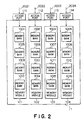
memory device 11 comprises a plurality ofmemory modules 101 to 104. Thememory modules 101 to 104 haveaccess ports 111 to 114, respectively, so as to be accessed separately. Each of thememory modules 101 to 104 comprises a first predetermined number ofmemory banks memory banks 1001 to 1016 have access ports (not shown), respectively, so as to be accessed. Each of thememory banks 1001 to 1016 comprises a second predetermined number of memory elements (not shown). - Turning back to Fig. 1, the memory
access control device 10 comprises an addresssignal processing unit 13. The addresssignal processing unit 13 is connected through the twoports second processors second processors - Turning to Fig. 3, the first input address signal comprises a first module address portion, a first bank address portion, and a first input element address portion. The first module address portion has two bits. The first bank address portion has two bits. The first element address portion has twelve bits.
- The second input address signal comprises a second module address portion, a second bank address portion, and a second element address portion. The second module address portion has two bits. The second bank address portion has two bits. The second element address portion has twelve bits.
- Turning back to Fig. 1, the address
signal processing unit 13 comprises first andsecond registers first register 131 is supplied with the first input address signal from thefirst processor 121 through theport 123. Thesecond register 132 is supplied with the second input address signal from thesecond processor 122 through theport 124. The addresssignal processing unit 13 processes the first and the second module address portions into first and second module address signals, each of which represents one of addresses of thememory modules 101 to 104, the first and the second bank address portions into first and the second bank address signals, each of which represents one of addresses of thememory banks 1001 to 1016, and produces the first and the second input address signals as first and second address signals, as they are. The first and the second input address signals are equal to, or identical with, the first and the second address signals. - A first bank address
signal holding circuit 14 comprises a plurality of gate circuits (not shown) and is a part of thefirst register 131. This part of thefirst register 131 holds the first bank address portion of the first bank address signal. The first bank addresssignal holding circuit 14 holds the first bank address portion of the first bank address signal as a first bank address held signal. A second bank addresssignal holding circuit 15 comprises a plurality of gate circuits (not shown) and is a part of thesecond register 132. This part of thesecond register 132 holds the second bank address portion of the second bank address signal. The second bank addresssignal holding circuit 15 holds the second bank address portion of the second bank address signal as a second bank address held signal. - A
module checking circuit 16 is connected to the first and thesecond registers ports module checking circuit 16 is supplied with the first and the second module address signals from the first and thesecond registers - A first
bank checking unit 17 is connected to the first and thesecond registers ports signal holding circuit 14 through aport 141. A secondbank checking unit 18 is connected to the first and thesecond registers ports signal holding circuit 15 through aport 151. - Turning to Fig. 4, the first
bank checking unit 17 comprises a first bank accesssignal holding circuit 171 and a first bankaccess checking circuit 172. - The first bank access
signal holding circuit 171 is connected to the first bank address signal holding circuit 14 (Fig. 1) and comprises first throughthird access registers 1711 to 1713. Supplied with the first bank address held signal through theport 141, thefirst access register 1711 memorizes the first bank address held signal as a first memorized signal when thefirst access register 1711 receives the first shift signal which is substantially equal to one of the clock pulses. Supplied with the first memorized signal, thesecond access register 1712 memorizes the first memorized signal as a second memorized signal on reception of the first shift signal. Likewise, thethird access register 1713 memorizes the second memorized signal as a third memorized signal on reception of the first shift signal. Thus, the first bank accesssignal holding circuit 171 holds a first bank access held signal which is a combination of the first through the third memorized signals. - The
memory device 11 is supplied with data from thefirst processor 121. Thememory device 11 has a memory access time Ta in which thememory device 11 has memorized the data from thefirst processor 121. It is assumed that the period between two ones of the clock pulses is equal to a quarter of the memory access time Ta. In this case, thefirst processor 121 can access different four ones of thememory banks 1001 to 1016 that are included indifferent memory modules 101 to 104 in the memory access time Ta. Consequently, the first bank accesssignal holding circuit 171 comprises the first through thethird access registers 1711 to 1713 which memorize the first through the third memorized signals each of which indicates one of thememory banks 1001 to 1016 that is accessed by thefirst processor 121. - The first bank
access checking circuit 172 is connected to the first and thesecond registers ports third access registers 1711 to 1713 through threeports 1715 to 1717. The first bankaccess checking circuit 172 comprises first throughsixth comparators 1721 to 1726 and two ORgates - The
first comparator 1721 is connected to the first register 131 (Fig. 1) and thefirst access register 1711 through theport 135 and theport 1715. Thefirst comparator 1721 is supplied with the first bank address signal and the first memorized signal through theports - The
second comparator 1722 is connected to the second register 132 (Fig. 1) and thefirst access register 1711 through theports first comparator 1722 is supplied with the second bank address signal and the first memorized signal through theports - The
third comparator 1723 is connected to the first register 131 (Fig. 1) and thesecond access register 1712 through theports third comparator 1723 is supplied with the first bank address signal and the second memorized signal through theports - The
fourth comparator 1724 is connected to the second register 132 (Fig. 1) and thesecond access register 1712 through theports fourth comparator 1724 is supplied with the second bank address signal and the second memorized signal through theports - The
fifth comparator 1725 is connected to the first register 131 (Fig. 1) and thethird access register 1713 through theports fifth comparator 1725 is supplied with the first bank address signal and the third memorized signal through theports - The
sixth comparator 1726 is connected to the second register 132 (Fig. 1) and thethird access register 1713 through theports sixth comparator 1726 is supplied with the second bank address signal and the third memorized signal through theports - The
OR gate 1727 is connected to the first, the third, and thefifth comparators ports OR gate 1727 is supplied with the first, the third, and the fifth access coincidence signal through theports port 1710. - The
OR gate 1728 is connected to the second, the fourth, and thesixth comparators ports OR gate 1728 is supplied with the second, the fourth, and the sixth access coincidence signal through theports port 1720. - Thus, the first bank
access checking circuit 172 checks the first bank address signal and the first bank access held signal to produce the first bank coincidence signal when the first bank address signal and the first bank access held signal coincide with each other. The first bankaccess checking circuit 172 checks the second bank address signal and the first bank access held signal to produce the second bank coincidence signal when the second bank address signal and the first bank access held signal coincide with each other. - Turning to Fig. 5, the second
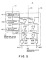
bank checking unit 18 comprises a second bank accesssignal holding circuit 181 and a second bankaccess checking circuit 182. - The second bank access
signal holding circuit 181 is connected to the second bank address signal holding circuit 15 (Fig. 1) and comprises fourth throughsixth access registers 1811 to 1813. Supplied with the second bank address held signal through theport 151, thefourth access register 1811 memorizes the second bank address held signal as a fourth memorized signal when thefourth access register 1811 receives the second shift signal which is substantially equal to one of the clock pulses. Supplied with the fourth memorized signal, thefifth access register 1812 memorized the fourth memorized signal as a fifth memorized signal on reception of the second shift signal. Likewise, thesixth access register 1813 memorizes the fifth memorized signal as a sixth memorized signal on reception of the second shift signal. Thus, the second bank accesssignal holding circuit 181 holds a second bank access held signal which is a combination of the fourth through the sixth memorized signals. - The
memory device 11 is supplied with data from thesecond processor 122. Thememory device 11 has the memory access time Ta in which thememory device 11 has memorized the data from thesecond processor 122. It is assumed that the period between two ones of the clock pulses is equal to a quarter of the memory access time Ta. In this case, thesecond processor 122 can access different four ones of thememory banks 1001 to 1016 that are included indifferent memory modules 101 to 104 in the memory access time Ta. Consequently, the second bank accesssignal holding circuit 181 comprises the fourth through thesixth access registers 1811 to 1813 which memorize the fourth through the sixth memorized signals each of which indicates one of thememory banks 1001 to 1016 that is accessed by thesecond processor 122. - The second bank
access checking circuit 182 is connected to the first and thesecond registers ports sixth access registers 1811 to 1813 through threeports 1815 to 1817. The first bankaccess checking circuit 182 comprises seventh throughtwelfth comparators 1821 to 1826 and two ORgates - The
seventh comparator 1821 is connected to the first register 131 (Fig. 1) and thefourth access register 1811 through theports fourth comparator 1821 is supplied with the first bank address signal and the fourth memorized signal through theports - The
eighth comparator 1822 is connected to the second register 132 (Fig. 1) and thefourth access register 1811 through theports eighth comparator 1822 is supplied with the second bank address signal and the fourth memorized signal through theports - The
ninth comparator 1823 is connected to the first register 131 (Fig. 1) and thefifth access register 1812 through theports ninth comparator 1823 is supplied with the first bank address signal and the fifth memorized signal through theports - The
tenth comparator 1824 is connected to the second register 132 (Fig. 1) and thefifth access register 1812 through theports tenth comparator 1824 is supplied with the second bank address signal and the fifth memorized signal through theports - The
eleventh comparator 1825 is connected to the first register 131 (Fig. 1) and thesixth access register 1813 through theports eleventh comparator 1825 is supplied with the first bank address signal and the sixth memorized signal through theports - The
twelfth comparator 1826 is connected to the second register 132 (Fig. 1) and thesixth access register 1813 through theports twelfth comparator 1826 is supplied with the second bank address signal and the sixth memorized signal through theports - The
OR gate 1827 is connected to the seventh, the ninth, and theeleventh comparators ports OR gate 1827 is supplied with the seventh, the ninth, and the eleventh access coincidence signal through theports port 1810. - The
OR gate 1828 is connected to the eighth, the tenth, and thetwelfth comparators ports OR gate 1828 is supplied with the eighth, the tenth, and the twelfth access coincidence signal through theports port 1820. - Thus, the second bank
access checking circuit 182 checks the first bank address signal and the second bank access held signal to produce the first bank coincidence signal when the first bank address signal and the second bank access held signal coincide with each other. The second bankaccess checking circuit 182 checks the second bank address signal and the second bank access held signal to produce the second bank coincidence signal when the second bank address signal and the second bank access held signal coincide with each other. - Turning back to Fig. 1, a judging
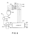
unit 19 is connected to themodule checking circuit 16 and the first and the secondbank checking units ports unit 19 comprises anaccess judging circuit 191 and a shiftsignal supply circuit 193. - Turning to Fig. 6, the
access judging circuit 191 comprises a judgingcircuit 1911, a first ANDgate 1912, a second ANDgate 1913, and amodule flag generator 1914. The first ANDgate 1912 is connected to theports inverters 1915 to 1918. The first ANDgate 1912 is supplied with the first bank coincidence signal from the first bank checking unit 17 (Fig. 1) through theport 1710 and theinverter 1915, with the second bank coincidence signal from the first bank checking unit 17 (Fig. 1) through theport 1720 and theinverter 1916, with the first bank coincidence signal from the second bank checking unit 18 (Fig. 1) through theport 1810 and theinverter 1917, and with the second bank coincidence signal from the second bank checking unit 18 (Fig. 1) through 5 theport 1820 and theinverter 1918 and outputs a first AND signal through aport 1919. - The second AND
gate 1913 is connected to the first ANDgate 1912 and the module checking circuit 16 (Fig. 1) through theports gate 1913 is supplied with the first AND signal and the module coincidence signal from the first ANDgate 1912 and the module checking circuit 16 (Fig. 1) through theports port 1920. - The
module flag generator 1914 is connected to the second ANDgate 1913 through theport 1920. An input port and an output port of themodule flag generator 1914 are connected to each other through aninverter 1921. Themodule flag generator 1914 is supplied with the second AND signal from the second ANDgate 1913 through theport 1920 and outputs a flag signal through aport 1922. - The judging
circuit 1911 is connected to the firstbank checking unit 17, the second bank checking unit 18 (Fig. 1), and themodule flag generator 1914 through theports circuit 1911 comprises a plurality of gate circuits (not shown). The judgingcircuit 1911 is supplied with the first bank coincidence signal from the first bank checking unit 17 (Fig. 1) through theport 1710, with the second bank coincidence signal from the first bank checking unit 17 (Fig. 1) through theport 1720, with the first bank coincidence signal from the second bank checking unit 18 (Fig. 1) through theport 1810, with the second bank coincidence signal from the second bank checking unit 18 (Fig. 1) through theport 1820, and with the flag signal from themodule flag generator 1914 through theport 1922 and outputs a first inhibit signal and a second inhibit signal through twoports - Turning back to Fig. 1, the shift
signal supply circuit 193 is connected to theaccess judging circuit 191 through theports signal holding circuit 14 and the second bank addresssignal holding circuit 15 through twoports signal supply circuit 193 comprises a plurality of gate circuits (not shown) and outputs the first shift signal and the second shift signal through theports - A truth table of the judging
unit 19 is illustrated in Figs. 7 and 8. In the truth table,symbols access control device 10 illustrated in Fig. 1. - As is apparent from the truth table (Figs. 7 and 8), the
access judging circuit 191 alternatingly produces the first inhibit signal and the second inhibit signal when supplied with the module coincidence signal, produces the first inhibit signal when supplied with the first bank coincidence signal, and produces the second inhibit signal when supplied with the second bank coincidence signal. Theaccess judging circuit 191 outputs the first and the second inhibit signals through theports signal supply circuit 193 produces the first shift signal when theaccess judging circuit 191 does not produce the first inhibit signal. The shiftsignal supply circuit 193 produces the second shift signal when theaccess judging circuit 191 does not produce the second inhibit signal. - Turning back to Fig. 1, the shift
signal supply circuit 193 uses the first and the second shift signal in transferring the first bank address held signal to the first bank access signal holding circuit 171 (Fig. 4) as the first bank access held signal, and the second bank address held signal to the second bank access signal holding circuit 181 (Fig. 5) as the second bank access held signal. - The address
signal processing unit 13 further comprises a first and a second input flag generator (not shown). The first input flag generator is connected to thefirst processor 121 and theaccess judging circuit 191 through aport 125 of the memoryaccess control device 10 and through theport 1923. The second input flag generator is connected to thesecond processor 122 and theaccess judging circuit 191 through alike port 126 and theport 1924. When the first input flag generator is supplied with the first inhibit signal from theaccess judging circuit 191 through theport 1923, the first input flag generator produces a first input inhibit signal which inhibits supply of the first input address signal to thefirst register 131 and supplies the first input inhibit signal to thefirst processor 121. When the second input flag generator is supplied with the second inhihit signal from theaccess judging circuit 191 through theport 1924, the second input flag generator produces a second input inhibit signal which inhibits supply of the second input address signal to thesecond register 132 and supplies the second input inhibit signal to thesecond processor 122. - An access signal
output control unit 20 is connected to the addresssignal processing unit 13 and the judgingunit 19 through twoports signal processing unit 13 and through theports output control unit 20 comprises an accesssignal sending controller 201 and a specifyingcircuit 202. - The access
signal sending controller 201 is connected to the addresssignal processing unit 13 and the judgingunit 19 through the twoports ports signal sending controller 201 comprises a plurality of gate circuits (not shown). The accesssignal sending controller 201 sends the first input address signal to the specifyingcircuit 202 when theaccess sending controller 201 is supplied with the first input address signal through theport 137 and when theaccess judging circuit 191 does not produce the first inhibit signal. The accesssignal sending controller 201 sends the second input address signal to the specifyingcircuit 202 when the accesssignal sending controller 201 is supplied with the second input address signal through theport 138 and when theaccess judging circuit 191 does not produce the second inhibit signal. - The specifying
circuit 202 is connected to the accesssignal sending controller 201 through twoports memory modules 101 to 104 (Fig. 2) of thememory device 11 through fourports 2021 to 2024. The specifyingcircuit 202 comprises a plurality of gate circuits (not shown). - When the specifying
circuit 202 is supplied with the first address signal from the accesssignal sending controller 201 through theport 2011, the specifyingcircuit 202 specifies, as a first specified memory module and a first specified memory bank, a particular memory module of thememory modules 101 to 104 (Fig. 2) and a particular memory bank of thememory banks 1001 to 1016 in the particular memory module. It is to be noted that the particular memory module and the particular memory bank are collectively indicated by the first address signal. The specifyingcircuit 202 sends the first element address portion of the first address signal to the first specified memory bank of the first specified memory module. - When the specifying
circuit 202 is supplied with the second address signal from the accesssignal sendinq controller 201 through theport 2012, thespecifyinq circuit 202 specifies, as a second specified memory module and a second specified memory bank, a specific memory module of thememory modules 101 to 104 (Fig. 2) and a specific memory bank of thememory banks 1001 to 1016 in the specific memory module. The specific memory module and the specific memory bank are collectively indicated by the second address signal. The specifyingcircuit 202 sends the second element address portion of the second address signal to the second specified memory bank of the second specified memory module. - The
memory device 11 is connected to thefirst processor 121 through twoports second processor 122 through twodifferent ports memory device 11 is supplied with a readout demand signal, a write demand signal, and the data from the first and thesecond processors second processors memory device 11.
Claims (4)
- A memory access control device which is for controlling access to a memory device (11) comprising first to N-th memory modules (101-104), where N represents an integer greater than 3, each of said memory modules comprising a predetermined number of memory banks, characterized by:a) address signal processing means (13) supplied with a first input address signal comprising a first module address portion, a first bank address portion, and a first element address portion and a second input address signal comprising a second module address portion, a second bank address portion, and a second element address portion for processing said first and said second module address portions into first and second module address signals each of which represents one of addresses of said memory modules, said first and said second bank address portions into first and second bank address signals each of which represents one of addresses of said memory banks, and for producing, said first and said second input address signals as first and second address signals as they are,b) a first bank address signal holding circuit (14) connected to said address signal processing means for holding said first bank address signal as a first bank address held signal;c) a second bank address signal holding circuit (15) connected to said address signal processing means for holding said second bank address signal as a second bank address held signal;d) a module checking circuit (16) connected to said address signal processing means for checking said first and said second module address signals to produce a module coincidence signal when said first and said second module address signals coincide with each other;e) a first bank access signal holding circuit (171) connected to said first bank address signal holding circuit for holding a first bank access held signal;f) a second bank access signal holding circuit (181) connected to said second bank address signal holding circuit for holding a second bank access held signal;g) a first bank access checking (172) circuit connected to said address signal processing means and said first bank access signal holding circuit for checking said first bank address signal and said first bank access held signal to produce a first bank coincidence signal when said first bank address signal and said first bank access held signal coincide with each other;h) a second bank access checking circuit (182) connected to said address signal processing means and said second bank access signal holding circuit for checking said second bank address signal and said second bank access held signal to produce a second bank coincidence signal when said second bank address signal and said second bank access held signal coincide with each other;i) access judging means (191) connected to said module checking circuit and said first and said second bank access checking circuits for alternatingly producing a first inhibit signal and a second inhibit signal when supplied with said module coincidence signal, said access judging means producing said first inhibit signal when supplied with said first bank coincidence signal, said access judging means producing said second inhibit signal when supplied with said second bank coincidence signal, and said access judging means producing first and second shift signals when said first and said second inhibit signals are not produced, respectively;j) shift signal supply means (193) connected to said access judging means and said first and said second bank address signal holding circuits for using said first and said second shift signals in transferring said first bank address held signal to said first bank access signal holding circuit as said first bank access held signal, and said second bank address held signal to said second bank access signal holding circuit as said second bank access held signal; andk) access signal output control means (20) connected to said memory modules, said address signal processing means, and said access judging means for specifying by said first address signal, as a first specified memory module, a particular memory module of said memory modules to send said first bank address portion and said first element address portion to said first specified memory module when said access signal output control means is supplied with said first address signal and when said access judging means does not produce said first inhibit signal, said access signal output control means specifying by said second address signal, as a second specified memory module, a specific memory module of said memory modules to send said second bank address portion and said second element address portion to said second specified memory module when said access signal output control means is supplied with said second address signal and when said access judging means does not produce said second inhibit signal.
- A memory access control device as claimed in Claim 1, characterized in that said access signal output control means is for inhibiting supply of aid first and said second address signals to said memory modules when said access judging means produces said first inhibit signal and when said access judging means produces said second inhibit signal, respectively.
- A memory access control device as claimed in Claim 1, characterized in that said access signal output control means is for specifying by said first address signal, as said first specified memory module and a first specified memory bank, said particular memory module of said memory modules and a particular memory bank of said predetermined number of memory banks in said particular memory module to send said first element address portion to said first specified memory bank of said first specified memory module when said access signal output control means is supplied with said first address signal and when said access judging means does not produce said first inhibit signal, said access signal output control means specifying by said second address signal, as said second specified memory module and a second specified memory bank, said specific memory module of said memory modules and a specific memory bank of said predetermined number of memory banks in said specific memory module to send said second element address portion to said second specified memory bank of said second specified memory module when said access signal output control means is supplied with said second address signal and when said access judging means does not produce said second inhibit signal.
- A memory access control device as claimed in Claim 3, characterized in that said access signal output control means is for inhibiting supply of said first and said second address signals to said memory modules when said access judging means produces said first inhibit signal and when said access judging means produces said second inhibit signal, respectively.
Applications Claiming Priority (2)
| Application Number | Priority Date | Filing Date | Title |
|---|---|---|---|
| JP2035704A JPH03238539A (en) | 1990-02-15 | 1990-02-15 | Memory access controller |
| JP35704/90 | 1990-02-15 |
Publications (3)
| Publication Number | Publication Date |
|---|---|
| EP0442496A2 EP0442496A2 (en) | 1991-08-21 |
| EP0442496A3 EP0442496A3 (en) | 1992-01-29 |
| EP0442496B1 true EP0442496B1 (en) | 1997-10-15 |
Family
ID=12449258
Family Applications (1)
| Application Number | Title | Priority Date | Filing Date |
|---|---|---|---|
| EP91102100A Expired - Lifetime EP0442496B1 (en) | 1990-02-15 | 1991-02-14 | Memory access control device having bank access checking circuits smaller in number than the memory modules |
Country Status (4)
| Country | Link |
|---|---|
| US (1) | US5293604A (en) |
| EP (1) | EP0442496B1 (en) |
| JP (1) | JPH03238539A (en) |
| DE (1) | DE69127914T2 (en) |
Families Citing this family (6)
| Publication number | Priority date | Publication date | Assignee | Title |
|---|---|---|---|---|
| DE69316955T2 (en) | 1992-09-18 | 1998-07-30 | Hitachi Ltd | Computer system with synchronous, dynamic memory |
| JP3010947B2 (en) * | 1992-11-26 | 2000-02-21 | 日本電気株式会社 | Memory access control device |
| US5949997A (en) * | 1997-01-03 | 1999-09-07 | Ncr Corporation | Method and apparatus for programming a microprocessor using an address decode circuit |
| EP0935199B1 (en) | 1998-02-04 | 2011-05-04 | Panasonic Corporation | Memory control unit and memory control method and medium containing program for realizing the same |
| US20070150667A1 (en) * | 2005-12-23 | 2007-06-28 | Intel Corporation | Multiported memory with ports mapped to bank sets |
| WO2012080556A1 (en) * | 2010-12-13 | 2012-06-21 | Nokia Corporation | Method and apparatus for 3d capture syncronization |
Family Cites Families (5)
| Publication number | Priority date | Publication date | Assignee | Title |
|---|---|---|---|---|
| US3601812A (en) * | 1969-01-22 | 1971-08-24 | Rca Corp | Memory system |
| JPS5128450B2 (en) * | 1971-10-06 | 1976-08-19 | ||
| JPS57211659A (en) * | 1981-06-23 | 1982-12-25 | Fujitsu Ltd | Memory access controller |
| US4745545A (en) * | 1985-06-28 | 1988-05-17 | Cray Research, Inc. | Memory reference control in a multiprocessor |
| US5167028A (en) * | 1989-11-13 | 1992-11-24 | Lucid Corporation | System for controlling task operation of slave processor by switching access to shared memory banks by master processor |
-
1990
- 1990-02-15 JP JP2035704A patent/JPH03238539A/en active Pending
-
1991
- 1991-02-14 EP EP91102100A patent/EP0442496B1/en not_active Expired - Lifetime
- 1991-02-14 DE DE69127914T patent/DE69127914T2/en not_active Expired - Fee Related
- 1991-02-15 US US07/655,947 patent/US5293604A/en not_active Expired - Fee Related
Also Published As
| Publication number | Publication date |
|---|---|
| US5293604A (en) | 1994-03-08 |
| DE69127914D1 (en) | 1997-11-20 |
| JPH03238539A (en) | 1991-10-24 |
| EP0442496A2 (en) | 1991-08-21 |
| EP0442496A3 (en) | 1992-01-29 |
| DE69127914T2 (en) | 1998-02-12 |
Similar Documents
| Publication | Publication Date | Title |
|---|---|---|
| EP0020908B1 (en) | Data processing system comprising a common bus communication system in which the width of the address field is greater than the number of lines on the bus | |
| US5345573A (en) | High speed burst read address generation with high speed transfer | |
| US5437019A (en) | Addressing method and apparatus for a computer system | |
| US3934227A (en) | Memory correction system | |
| EP0518488A1 (en) | Bus interface and processing system | |
| US4825404A (en) | Interface system which generates configuration control signal and duplex control signal for automatically determining the configuration of removable modules | |
| US4115854A (en) | Channel bus controller | |
| GB2215497A (en) | Self configuring memory system | |
| CA2052559C (en) | Vector processing device comprising a reduced amount of hardware | |
| EP0442496B1 (en) | Memory access control device having bank access checking circuits smaller in number than the memory modules | |
| EP0454836B1 (en) | System for memory data integrity | |
| US5020013A (en) | Bidirectional variable bit shifter | |
| US7355917B2 (en) | Two-dimensional data memory | |
| US4162534A (en) | Parallel alignment network for d-ordered vector elements | |
| GB2241598A (en) | Six-way access ported ram array cell | |
| US5327362A (en) | System for detecting a runaway of a microcomputer | |
| EP0283230B1 (en) | A register circuit | |
| US5414721A (en) | Serial data receiving device | |
| US6292882B1 (en) | Method and apparatus for filtering valid information for downstream processing | |
| RU2054710C1 (en) | Multiprocessor control system | |
| US4151375A (en) | System for selectively shifting groups of bits for temporary storage in a processor memory of a telephone exchange | |
| US3702463A (en) | Data processor with conditionally supplied clock signals | |
| CA1076708A (en) | Parallel bidirectional shifter | |
| EP0192209B1 (en) | Address contention arbitrator for multi-port memories | |
| US5845131A (en) | Multiprocessor system employing an improved self-coded distributed interrupt arbitration technique |
Legal Events
| Date | Code | Title | Description |
|---|---|---|---|
| PUAI | Public reference made under article 153(3) epc to a published international application that has entered the european phase |
Free format text: ORIGINAL CODE: 0009012 |
|
| 17P | Request for examination filed |
Effective date: 19910311 |
|
| AK | Designated contracting states |
Kind code of ref document: A2 Designated state(s): BE DE FR GB IT NL SE |
|
| PUAL | Search report despatched |
Free format text: ORIGINAL CODE: 0009013 |
|
| AK | Designated contracting states |
Kind code of ref document: A3 Designated state(s): BE DE FR GB IT NL SE |
|
| 17Q | First examination report despatched |
Effective date: 19940919 |
|
| GRAH | Despatch of communication of intention to grant a patent |
Free format text: ORIGINAL CODE: EPIDOS IGRA |
|
| GRAH | Despatch of communication of intention to grant a patent |
Free format text: ORIGINAL CODE: EPIDOS IGRA |
|
| GRAA | (expected) grant |
Free format text: ORIGINAL CODE: 0009210 |
|
| AK | Designated contracting states |
Kind code of ref document: B1 Designated state(s): BE DE FR GB IT NL SE |
|
| REF | Corresponds to: |
Ref document number: 69127914 Country of ref document: DE Date of ref document: 19971120 |
|
| ITF | It: translation for a ep patent filed | ||
| ET | Fr: translation filed | ||
| PLBE | No opposition filed within time limit |
Free format text: ORIGINAL CODE: 0009261 |
|
| STAA | Information on the status of an ep patent application or granted ep patent |
Free format text: STATUS: NO OPPOSITION FILED WITHIN TIME LIMIT |
|
| 26N | No opposition filed | ||
| PGFP | Annual fee paid to national office [announced via postgrant information from national office to epo] |
Ref country code: SE Payment date: 19990204 Year of fee payment: 9 |
|
| PGFP | Annual fee paid to national office [announced via postgrant information from national office to epo] |
Ref country code: FR Payment date: 19990209 Year of fee payment: 9 |
|
| PGFP | Annual fee paid to national office [announced via postgrant information from national office to epo] |
Ref country code: GB Payment date: 19990218 Year of fee payment: 9 |
|
| PGFP | Annual fee paid to national office [announced via postgrant information from national office to epo] |
Ref country code: NL Payment date: 19990224 Year of fee payment: 9 |
|
| PGFP | Annual fee paid to national office [announced via postgrant information from national office to epo] |
Ref country code: DE Payment date: 19991231 Year of fee payment: 10 |
|
| PGFP | Annual fee paid to national office [announced via postgrant information from national office to epo] |
Ref country code: BE Payment date: 20000119 Year of fee payment: 10 |
|
| PG25 | Lapsed in a contracting state [announced via postgrant information from national office to epo] |
Ref country code: GB Free format text: LAPSE BECAUSE OF NON-PAYMENT OF DUE FEES Effective date: 20000214 |
|
| PG25 | Lapsed in a contracting state [announced via postgrant information from national office to epo] |
Ref country code: SE Free format text: LAPSE BECAUSE OF NON-PAYMENT OF DUE FEES Effective date: 20000215 |
|
| PG25 | Lapsed in a contracting state [announced via postgrant information from national office to epo] |
Ref country code: NL Free format text: LAPSE BECAUSE OF NON-PAYMENT OF DUE FEES Effective date: 20000901 |
|
| GBPC | Gb: european patent ceased through non-payment of renewal fee |
Effective date: 20000214 |
|
| EUG | Se: european patent has lapsed |
Ref document number: 91102100.4 |
|
| PG25 | Lapsed in a contracting state [announced via postgrant information from national office to epo] |
Ref country code: FR Free format text: LAPSE BECAUSE OF NON-PAYMENT OF DUE FEES Effective date: 20001031 |
|
| NLV4 | Nl: lapsed or anulled due to non-payment of the annual fee |
Effective date: 20000901 |
|
| REG | Reference to a national code |
Ref country code: FR Ref legal event code: ST |
|
| PG25 | Lapsed in a contracting state [announced via postgrant information from national office to epo] |
Ref country code: BE Free format text: LAPSE BECAUSE OF NON-PAYMENT OF DUE FEES Effective date: 20010228 |
|
| BERE | Be: lapsed |
Owner name: NEC CORP. Effective date: 20010228 |
|
| PG25 | Lapsed in a contracting state [announced via postgrant information from national office to epo] |
Ref country code: DE Free format text: LAPSE BECAUSE OF NON-PAYMENT OF DUE FEES Effective date: 20011201 |
|
| PG25 | Lapsed in a contracting state [announced via postgrant information from national office to epo] |
Ref country code: IT Free format text: LAPSE BECAUSE OF NON-PAYMENT OF DUE FEES;WARNING: LAPSES OF ITALIAN PATENTS WITH EFFECTIVE DATE BEFORE 2007 MAY HAVE OCCURRED AT ANY TIME BEFORE 2007. THE CORRECT EFFECTIVE DATE MAY BE DIFFERENT FROM THE ONE RECORDED. Effective date: 20050214 |