EP0442527A2 - Appareil de formation d'images - Google Patents
Appareil de formation d'images Download PDFInfo
- Publication number
- EP0442527A2 EP0442527A2 EP91102196A EP91102196A EP0442527A2 EP 0442527 A2 EP0442527 A2 EP 0442527A2 EP 91102196 A EP91102196 A EP 91102196A EP 91102196 A EP91102196 A EP 91102196A EP 0442527 A2 EP0442527 A2 EP 0442527A2
- Authority
- EP
- European Patent Office
- Prior art keywords
- control means
- constant
- voltage
- image
- charging
- Prior art date
- Legal status (The legal status is an assumption and is not a legal conclusion. Google has not performed a legal analysis and makes no representation as to the accuracy of the status listed.)
- Granted
Links
Images


Classifications
-
- G—PHYSICS
- G03—PHOTOGRAPHY; CINEMATOGRAPHY; ANALOGOUS TECHNIQUES USING WAVES OTHER THAN OPTICAL WAVES; ELECTROGRAPHY; HOLOGRAPHY
- G03G—ELECTROGRAPHY; ELECTROPHOTOGRAPHY; MAGNETOGRAPHY
- G03G15/00—Apparatus for electrographic processes using a charge pattern
- G03G15/14—Apparatus for electrographic processes using a charge pattern for transferring a pattern to a second base
- G03G15/16—Apparatus for electrographic processes using a charge pattern for transferring a pattern to a second base of a toner pattern, e.g. a powder pattern, e.g. magnetic transfer
- G03G15/1665—Apparatus for electrographic processes using a charge pattern for transferring a pattern to a second base of a toner pattern, e.g. a powder pattern, e.g. magnetic transfer by introducing the second base in the nip formed by the recording member and at least one transfer member, e.g. in combination with bias or heat
- G03G15/167—Apparatus for electrographic processes using a charge pattern for transferring a pattern to a second base of a toner pattern, e.g. a powder pattern, e.g. magnetic transfer by introducing the second base in the nip formed by the recording member and at least one transfer member, e.g. in combination with bias or heat at least one of the recording member or the transfer member being rotatable during the transfer
- G03G15/1675—Apparatus for electrographic processes using a charge pattern for transferring a pattern to a second base of a toner pattern, e.g. a powder pattern, e.g. magnetic transfer by introducing the second base in the nip formed by the recording member and at least one transfer member, e.g. in combination with bias or heat at least one of the recording member or the transfer member being rotatable during the transfer with means for controlling the bias applied in the transfer nip
Definitions
- the present invention relates to an image forming apparatus such as an electrophotographic copying machine or printer, more particularly to an image forming apparatus having a charging member such as a transfer roller.
- An image forming apparatus has been proposed in which a nip is formed between an image bearing member and a contact type transfer member such as a transfer roller press-contacted to the image bearing member, and a recording material is passed through the nip while the transfer bias is applied to the transfer member, so that the toner image formed on the image bearing member is transferred onto the recording material.
- a contact type transfer member such as a transfer roller press-contacted to the image bearing member
- the resistivity of the charging member remarkably varies by the ambience particularly humidity, and therefore, the transfer current flowing through the recording material varies when the transfer bias is applied.
- the change of the transfer current is significant when the size of the transfer material is changed. Therefore, it has been difficult to provide stabilized images.
- Figure 19 shows such a system.
- a photosensitive member is rotatable in a direction indicated by an arrow about an axis extending perpendicularly to the sheet of the drawing.
- a primary high voltage source 23 supplies power to a primary charger 2 which uniformly charges the photosensitive member 1.
- An image signal 3 in the form of light is applied to the photosensitive member so that an electrostatic latent image is formed.
- the charged toner is supplied to the latent image from a developing sleeve supplied with a developing bias from a high voltage source 24, by which a toner image is formed.
- the roller 5 When the toner image reaches an image transfer zone where the photosensitive member 1 and the transfer roller 5 are press-contacted, the roller 5 is supplied with an image transfer bias from a transfer high voltage source 36, so that the toner image is transferred from the photosensitive member to the recording material P, thereafter the recording material P is conveyed to an unshown image fixing device.
- the bias applied to the transfer roller 5 is controlled in the following manner.
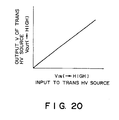
- the high voltage source 36 for the image transfer produces a voltage proportional to an analog level of the input signal, as shown in Figure 20.
- a constant current control circuit is constituted by the operational amplifier 38, the resistors 37, 43 and 44 and a capacitor 45.
- the analog switches 39 and 40 are rendered off, and the analog switch 41 is actuated. Therefore, the transfer high voltage source 36 is supplied with a voltage charged in the capacitor 47.
- the input impedance of the high voltage source 36 is sufficiently high so that the voltage drop through the capacitor 47 is small, and therefore, the capacitor 47 constitutes a constant voltage control circuit for the transfer roller.
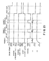
- Figure 21 illustrates the operational sequence in which the photosensitive member starts to rotate, and continuously produces three prints, and thereafter, the image forming operation terminates.
- the signals HVPON and HVDON become high to actuate a primary high voltage source 23, a developing high voltage source 24, and set the analog level CCNT for the constant current control to a predetermined level. Then, the transfer roller is constant-current-controlled in accordance with the level of the signal CCNT.
- the input voltage V1 to the transfer high voltage source 36 changes significantly, but the voltage across the capacitor 47 which is stored for the constant voltage control is determined at a point of time when the analog switch 40 is opened.
- the level of the signal CNTON becomes low, so that the transfer roller 5 is constant-current-controlled with the voltage stored in the capacitor 47.
- the voltage obtained during the constant current control of the transfer roller is stored by the charging of the capacitor, and during the constant voltage control, the transfer roller 5 is constant-voltage-controlled with the voltage stored in the capacitor.
- the constant voltage control is dependent on the capacitance of the capacitor in such an apparatus.
- the capacitance discharges with time, and therefore, the voltage level is not held for a long period of time.
- the transfer roller generally has different resistivities at different portions (circumferential direction of the roller, for example). Due to the variation in the resistance, and therefore, it is not assured that the proper voltage is applied to the transfer roller, even if the voltage applied to the transfer roller is determined during the constant current control.
- the level of the transfer bias is too high with the result of too strong electric field which may damage the image bearing member or which causes improper image transfer (local void).
- the voltage during the constant voltage control is determined on the basis of the low resistance portion of the transfer roller, the transfer bias becomes too low also with the result of improper image transfer.
- It is a yet further object of the present invention to provide an image forming apparatus comprising an A/D transducer for analog voltage level during the constant current control by a constant current control means is converted to a digital level, determining means for determining a digital level corresponding to a constant voltage level during the subsequent constant voltage control, on the basis of the converted digital level, and D/A transducer means for converting a digital level corresponding to the constant voltage level determined by the aforementioned means to an analog level, wherein the constant voltage control means is operated in accordance with the analog level provided by the D/A transducer means.
- Figure 1 is a system diagram of an apparatus according to a first embodiment of the present invention.
- Figure 2 is a timing chart of the operation of the apparatus of the first embodiment.
- Figure 3 is a graph illustrating the variation in the resistivity of the transfer roller.
- Figure 4 is a block diagram illustrating a second embodiment of the present invention.
- Figure 5 is a graph illustrating a content of a table functioning as a setting means usable with the present invention.
- Figure 6 is a system diagram of the apparatus according to a third embodiment of the present invention.
- Figure 7 is a system diagram used in a fourth and a fifth embodiments of the present invention.
- Figure 8 is a timing chart of the operation of the apparatus of the fourth embodiment.
- Figures 9 - 12 are timing charts for the apparatuses of the fourth and fifth embodiments.
- Figures 13 is a timing chart of the apparatus according to the fourth and fifth embodiments.
- Figure 14 is a flow chart illustrating sequential operation sin the apparatus SOS the fourth embodiment.
- Figure 15 is a flow chart of the sequential operations of the apparatus according to the fifth embodiment.
- Figure 16 illustrates a correcting method in the fifth embodiment.
- Figure 17 is a flow chart of the sequential operations of the apparatus according to a sixth embodiment of the present invention.
- Figure 18 illustrates a problem with A/D and D/A conversions.
- Figure 19 is a system diagram from which the present invention starts.
- Figure 20 is a graph showing the input-output of the voltage source in the apparatus of Figure 19.
- Figure 21 is a timing chart in the operation of the system of Figure 19.
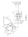
- FIG. 1 there is shown an image forming apparatus according to a first embodiment of the present invention.
- the apparatus shown has a rotatable cylindrical photosensitive member 1 having an axis extending perpendicularly to the sheet of the drawing.
- the photosensitive member 1 has a surface OPC photosensitive layer and is rotatable in the direction indicated by an arrow.
- the photosensitive layer is uniformly charged by a primary charger 2, and is exposed to a laser beam 3 which is modulated in accordance with an image.
- the electric potential of the photosensitive member is attenuated at the portion which has been exposed to the laser beam, so that an electrostatic latent image is formed.
- the photosensitive member imagewisely receives the negatively charged toner form the developing device 14, so that the latent image is reverse-developed into a toner image.
- an image transfer roller (charging member) 5 is press-contacted to the photosensitive member 1 to establish a charging zone.
- the transfer roller 5 is supplied from a bias means 9 with a positive transfer bias through a core metal 6 thereof, by which the toner image is transferred from the photosensitive member to the recording material. Thereafter, the transfer material P carrying the toner image is conveyed to an image fixing station (not shown).
- the material of the transfer roller 5 is, for example, an EPDM (of ethylene-, propylene- and diene-terpolymer) in which carbon is dispersed so as to provide a volume resistivity of 107 - 1010 ohm.cm and a hardness of 25 - 30 degrees (Asker C).
- EPDM of ethylene-, propylene- and diene-terpolymer
- the bias application means 9 comprises a high voltage source 10 for supplying electric power to the transfer roller 5, a constant current driver circuit (constant current control means) 11 for supplying a constant current to the transfer roller, a constant voltage driver circuit (constant voltage control means) 12 for supplying a constant voltage to the transfer roller, and a subordinate CPU 13 having a D/A converter to control it.
- the subordinate CPU 13 is controlled by a main CPU 14 having therein an A/D transducer and a memory.
- the subordinate CPU 13 supplies a predetermined constant current to the transfer roller 5 from the high voltage source 10 through a constant current driver circuit 14 during a pre-rotation period (timing chart of Figure 2).
- the voltage V T at this time is detected, and on the basis of the detected voltage, the voltage applied to the transfer roller 5 during the transfer operation in which the toner image is transferred from the image bearing member 1 to the recording material P, is controlled to a proper level.
- the constant current control operation is preferably performed when the toner image is not present in the transfer charging zone where the transfer roller is faced or contacted to the image bearing member, or when the recording material is not present in the developing zone.
- the constant current level supplied to the transfer roller 5 is approximately 30 micro-amperes.
- the transfer bias during the constant voltage image transfer operation is determined, and the image forming condition of image forming means is determined on the basis of the determined transfer bias voltage.
- the image forming condition includes a voltage supplied to the primary charger, the amount of exposure by the exposure means, a bias voltage applied to the developing means or the like.
- Figure 3 illustrates non-uniform resistivity in the circumferential direction of the transfer roller mentioned in the foregoing.
- the resistivity of the transfer roller so varies along one circumference A that the voltage produced thereby changes within a range from +2.7 to +3.3 KV. Without proper consideration to the fact, it is difficult to select proper and stabilized bias voltage.
- the voltage stored in the main CPU 16 during the constant current control is divided into 256 parts from which the respective voltage levels are read. Then, an average voltage level V T of the plural voltages is temporarily stored in the main CPU 14, and during the transfer operation in which the constant current control is performed, the stored voltage level is supplied to the subordinate CPU 13.
- the constant voltage driver circuit 12 drives the high voltage source 10 so that the voltage on the basis of the voltage level stored is supplied to the transfer roller. In other words, on the basis of the plural voltage levels produced during the constant current control operation by the constant current control means, the image forming condition of the image forming means is controlled by the CPU.
- the average may be determined from the data covering M circumferences (N is 0.5 or 2.3, for example). However, in consideration of the variation in the resistivity in the circumferential direction of the transfer roller, N is preferably integer.
- the non-uniform resistivity of the transfer roller may result from the contamination of the roller surface it is preferable that prior to the constant current control operation, a reversed bias voltage is applied to the transfer roller 5, as shown in Figure 2, so that the contamination toner is returned to the photosensitive member from the transfer roller surface.
- a reversed bias voltage is applied to the transfer roller 5, as shown in Figure 2, so that the contamination toner is returned to the photosensitive member from the transfer roller surface.
- good results were obtained by the reversed bias voltage of -1 - -2 KV approximately.
- a low level bias of +500 - 1 KV approximately is applied to the transfer roller, since then the photosensitive member is subjected to the transfer hysteresis which is substantially the same as the hysteresis when the transfer bias of approximately +3 KV is supplied to the photosensitive member through the recording material P, by which the surface potential of the photosensitive member after the image transfer is made uniform, and therefore, the non-uniformity of the residual charge on the photosensitive member after the image transfer operation can be avoided.
- the low level bias voltage may be obtained by multiplying the above-described bias voltage by ⁇ (0 ⁇ ⁇ ⁇ 1).
- a constant voltage control is effected to the transfer roller by a constant voltage driver circuit 12.
- the parameter corresponding to the resistivity of the transfer roller is detected from an average current i T obtained at different positions of the transfer roller for 1 - N circumferences.
- the transfer bias during the toner image transfer operation is determined. It is preferable that the currents i are detected at different positions of the transfer roller.
- the signals corresponding to one or more detected currents i is supplied from the voltage source 10 to an A/D converter of the main CPU 14, and the signal corresponding to the analog current level detected is stored in the CPU as a digital level. Then, the digital level is converted to an analog level by a D/A converter in the CPU, by which the proper transfer bias V TC is determined.
- the transfer roller is constant-voltage-controlled when the toner image is present in the charging zone or when the recording material is present in the charging zone.
- a look-up table shown in Figure 5 may be prepared in the main CPU 14 or in an external memory, from which the proper bias level is determined on the basis of the detected current level.
- the charging zone is provided by a photosensitive member 1 and a transfer belt 19 contacted thereto, the transfer belt 19 is stretched around a pair of supporting rollers 15 and 17.
- the toner image formed on the surface of the photosensitive member 1 reaches the charging zone.
- the recording material P is supplied to the charging zone on the transfer belt 19 from the right of Figure 6.
- the material of the transfer belt 19 may be PVdF (polyfluorinated vinylidene resin) having a side chain substituted with hydroxyl group, amide group or the like so that it has the intermediate resistivity similarly to the above-described transfer roller.
- PVdF polyfluorinated vinylidene resin
- the transfer belt 19 is supplied with the transfer bias means 9 through the core metal 16 and an external conductive layer 18, so as to effect the image transfer action.
- control bias is supplied as in the first embodiment.
- the transfer belt 19 is provided with a mark 20 at a proper position outside the recording material contacting zone.
- the mark is detected by a photosensor 21.
- the constant current is supplied to the transfer belt, and the voltage V supplied to the transfer belt is stored in the memory 22, for plural points along one or more (N) circumferences of the transfer belt 19 with sufficient resolution (in this case 256 points are detected).
- the transfer belt 19 is constant voltage controlled with the target voltages stored in the memory 22 corresponding to the position on the transfer belt 19 determined with reference to the mark.
- the constant voltage control is such that 256 constant large voltage levels corresponding to the non-uniformity of the resistivity of the transfer belt are used depending on the positions on the transfer belt.
- the transfer bias level can follow the local different resistivities of the transfer belt, even if the resistivity of the transfer belt 19 surface is non-uniform in its travel direction. Therefore, the image transfer performance is always stabilized.
- This follow-up system is usable to the transfer member of a roller type described in the foregoing.
- control bias has the same polarity as in the transfer operation.
- control bias may be a cleaning bias (opposite polarity), as described with the first embodiment.
- control step is effected during the pre-rotation. However, it may be performed immediately after the main switch is actuated, during a post rotation, or during the sheet interval or intervals.
- the apparatus comprises a photosensitive member 1, a rotatable transfer roller (charging member) 5 for transferring a toner image from the photosensitive member 1 to a recording material P, a transfer high voltage source 12 for supplying electric power to the transfer roller 5, a primary charger 2, a primary high voltage source 23 for supplying electric power thereto, a developing device 4 for developing a latent image formed on the photosensitive member 1 by an image exposure into a toner image and a high voltage source 24 for the developing device.
- the transfer roller 2 is faced or contacted to the photosensitive member 1.
- the apparatus further comprises a CPU 35 including an A/D transducer and a D/A transducer, operational amplifiers 25 and 26, diodes 27 and 28, resistors 29, 30 and 31 and a capacitor 32.
- a CPU 35 including an A/D transducer and a D/A transducer, operational amplifiers 25 and 26, diodes 27 and 28, resistors 29, 30 and 31 and a capacitor 32.
- An analog circuit including the operational amplifier 25, resistors 29 - 31 and the capacitor 35 constitutes a constant current control means 33 for constant-current-controls the transfer roller 5 so that the current supplied thereto is at a predetermined constant level.
- the operational amplifier 26 constitutes a constant voltage control means 34 for constant voltage control for the transfer roller 5 to supply a predetermined constant voltage to the transfer roller 5.
- the A/D converter in the CPU 35 functions to convert a detection signal corresponding to the analog voltage level obtained during the constant current control to a digital signal (digital level), and in accordance with the digital level, the CPU 35 determines a digital level corresponding to the constant voltage level to be supplied to the constant voltage control means.
- the CPU 35 first determines a target level (predetermined constant level) for the constant current control in response to an output signal CCNT of the D/A converter. At this time, the output VCNT of the other D/A is 0. With this state, the transfer roller 5 is constant-current-controlled.
- the constant current control means is performed when the image bearing member does not have the toner image in the charging zone where the charging member is faced to the image bearing member. In other words, the constant current control is effected when the recording material is not present in the charging zone.
- the input signal Y IN to the transfer high voltage source 12 is supplied to A/D port of the CPU 35.
- the CPU 35 samples a plurality of times (256 times, for example) the input signals V IN during one full rotation of the transfer roller 5, and the A/D transducer means converts the plural analog voltage levels to the respective digital levels. Then, the CPU 35 determines an average of the plural digital levels read in.
- One of the D/A output signals CCNT is used as a voltage source voltage V BB during the image forming operation.
- the plural analog voltage levels may be obtained from different positions of the transfer roller irrespective of the number of rotations of the transfer roller.
- the CPU 35 Upon start of the printing operation, the CPU 35 produces an output VCNT through the D/A transducer means for converting to an analog level the digital level corresponding to the constant current level determined by the CPU 35.
- the operational amplifier 26 functions as a voltage follower, and the VCNT signal is supplied to the transfer high voltage source 12.
- the transfer roller 5 is constant-voltage-controlled with the voltage proportional to the input signal VCNT.
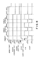
- Figure 8 shows sequential operations when three prints are produced continuously.
- the photosensitive member 1 Before starting the printing operation, the photosensitive member 1 is started for the pre-rotation (prior to the start of the image forming operation).
- the primary voltage source 23 and the developer high voltage source 24 are actuated, and the D/A output signal CCNT of the CPU 35 is set to a target level for the constant current control.
- an average of the input signals V IN of the transfer high voltage source 12 is determined, and thereafter, the output signal CCNT is returned to the voltage source V BB , and when the potential of the photosensitive member 1 which is non-uniform due to the constant current control is made uniform, the image forming operation is started.
- the target level of the constant voltage control is stored in the CPU 35.
- the target level is produced as an output signal VCNT, and the image transfer operation is effected. Then, the constant current control operation in the sheet intervals becomes unnecessary, and therefore, the good image forming operation can be effected in the continuous printing mode without reducing the throughput of the operation.
- the constant current control is performed with a digital circuit using the CPU, the response is slow with the possible result of oscillation of the output voltage due to the non-uniformity of the roller surface resistivity in the transfer roller 5.
- the constant current control for the transfer roller 3 is carried out using an analog circuit having a high response speed, and therefore, there is no liability of the oscillation.
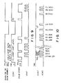
- the voltage obtained as a result of the constant current control changes mainly in accordance with the change in the ambient conditions, and therefore, the sequential control when a substantial number of prints are to be produced, may be as follows. If the ambient conditions inside the apparatus are predicted not to be significantly changed, the constant current control is effected immediately after the main switch is actuated ( Figure 9), and thereafter, the subsequent image transfer operation is effected on the basis of the voltage determined at that time, until the main switch is deactuated. Alternatively, as shown in Figure 10, the number of prints is counted, and the constant current control is performed, and the transfer voltage is renewed, for every 1000 prints, for example. Further alternatively, as shown in Figure 11, a timer is used to carry out the constant current control for every one hours, for example. Then, the similar advantageous effects are provided, as the case may be.
- the digital level may be converted to the analog level by passing a signal through a low pass filter, as shown in Figure 12.
- the output signal CCND of the CPU 35 is set to a predetermined level at step S1, thus starting the constant current control for the transfer roller 5.
- the monitor input voltages V IN of the transfer high voltage source 12 is sampled a plurality of times (256 times during one full turn, for example, of the transfer roller 5).
- the output signal CCND is reset, by which the constant current control of the transfer roller 5 is terminated.
- step S4 a constant voltage signal (D/A converted digital data DVCNT for obtaining an output signal VCNT to be supplied to the operational amplifier 26) from an average of the digital data VD IN of the transfer voltage V IN obtained by A/D conversion after the above-described sampling.
- the target level during the constant voltage control is determined (A of Figure 13). Then, the transfer voltage control is started at step S5.
- the actual output voltage V2 from the VCNT is different from the theoretical output voltage V1 if an error occurs by the passage of the signal through the D/A transducer and the A/D transducer.
- a fifth embodiment provides an image forming apparatus comprising correcting means in consideration of the error produced by the A/D converting means and the D/A converting means.
- step S5 The description will be made as to the correction of the error.
- the operation up to the step S5 is the same as in the fourth embodiment, and therefore, the detailed description thereof is omitted.
- the output signal VCNT is set as the target level which represents a constant voltage level to be supplied to the transfer roller, and the constant voltage control operation is started.
- the transfer voltage V IN at this time is sampled (three times, for example), and an average is obtained (B of Figure 13). Since the transfer voltage V IN is stable at this time, it is not necessary to sample a great number of times as in the constant current control sampling.
- the output signal VCNT is reset at step S7, and the constant voltage control is terminated.
- the target level of the constant voltage control that is, the constant voltage control signal is corrected.
- FIG 16 illustrates the correction of the constant voltage control signal.
- the VCNT voltage (V IN voltage) V3 upon the output of DV3 is very close to V1.
- the image forming process is performed through the usual electrophotographic process, as shown in Figure 13.
- the constant voltage level to be supplied to the transfer rollers is corrected to be closer to the target level corresponding to the analog level produced during the constant current control or to the analog level produced during the constant current control; or the analog level as a result of the D/A conversion is made closer to the analog level produced during the constant current control operation.
- FIG 17 is a flow chart of sequential operations of the apparatus of a sixth embodiment.
- the operations at steps S1 - S3 are the same as those during the constant current control in the steps S1 - S3 in Figure 15.
- an average of the data DV IN obtained as a result of the sampling at the step S2 is stored in the CPU 11 as a reference data DV INref and as D/A conversion data DVCNT.
- an output signal (voltage) VCNT is produced by D/A conversion of the data DVCNT.
- the constant voltage control is started.
- the sampling of the voltage V IN (reading of the data DV IN ) is carried out.
- step S14 the description is made as to whether or not the difference
- the more accurate constant voltage control voltage is determined than in the foregoing embodiments.
- An image forming apparatus includes an image forming device for forming an image on a recording material, the image forming device including an image bearing member, a movable charging member for charging the image bearing member and a power source for supplying electric power to the charging member; a constant current controller for supplying the charging member with a predetermined constant level of electric current; and a second controller for controlling an image forming condition by the image forming device on the basis of plural voltages provided at different points of time during a constant current control operation with the same constant current level by the constant current controller.
Landscapes
- Physics & Mathematics (AREA)
- General Physics & Mathematics (AREA)
- Electrostatic Charge, Transfer And Separation In Electrography (AREA)
Applications Claiming Priority (6)
| Application Number | Priority Date | Filing Date | Title |
|---|---|---|---|
| JP33698/90 | 1990-02-16 | ||
| JP2033698A JPH03238485A (ja) | 1990-02-16 | 1990-02-16 | 画像形成装置 |
| JP124170/90 | 1990-05-16 | ||
| JP12417090A JPH0420983A (ja) | 1990-05-16 | 1990-05-16 | 画像形成装置の転写装置 |
| JP2242568A JP3032897B2 (ja) | 1990-09-14 | 1990-09-14 | 画像形成装置 |
| JP242568/90 | 1990-09-14 |
Publications (3)
| Publication Number | Publication Date |
|---|---|
| EP0442527A2 true EP0442527A2 (fr) | 1991-08-21 |
| EP0442527A3 EP0442527A3 (en) | 1992-10-07 |
| EP0442527B1 EP0442527B1 (fr) | 1998-11-25 |
Family
ID=27288175
Family Applications (1)
| Application Number | Title | Priority Date | Filing Date |
|---|---|---|---|
| EP91102196A Expired - Lifetime EP0442527B1 (fr) | 1990-02-16 | 1991-02-15 | Appareil de formation d'images |
Country Status (3)
| Country | Link |
|---|---|
| US (1) | US5196885A (fr) |
| EP (1) | EP0442527B1 (fr) |
| DE (1) | DE69130511T2 (fr) |
Cited By (9)
| Publication number | Priority date | Publication date | Assignee | Title |
|---|---|---|---|---|
| EP0520819A3 (en) * | 1991-06-28 | 1993-05-26 | Canon Kabushiki Kaisha | Image forming apparatus having charging member |
| EP0522812A3 (en) * | 1991-07-06 | 1993-07-28 | Fujitsu Limited | Image transferring device |
| EP0552730A3 (fr) * | 1992-01-22 | 1994-04-27 | Ricoh Kk | |
| EP0584836A3 (fr) * | 1992-08-28 | 1995-04-12 | Canon Kk | Appareil de formation d'images pour la formation d'images sur deux faces d'un matériau d'enregistrement. |
| US5461461A (en) * | 1992-01-22 | 1995-10-24 | Ricoh Company, Ltd. | Image transferring device and medium separating device for an image forming apparatus |
| US5557384A (en) * | 1992-01-22 | 1996-09-17 | Ricoh Company, Ltd. | Image transferring device for image forming equipment |
| US5659843A (en) * | 1992-01-22 | 1997-08-19 | Ricoh Company, Ltd. | Image transferring device for image forming equipment |
| WO1999034260A1 (fr) * | 1997-12-29 | 1999-07-08 | Eastman Kodak Company | Procede et appareil de formation d'image avec commande du transfert electronique par courant constant |
| EP2474867A3 (fr) * | 2011-01-06 | 2017-05-31 | S-Printing Solution Co., Ltd. | Appareil de formation d'images et procédé de commande de son alimentation de transfert |
Families Citing this family (32)
| Publication number | Priority date | Publication date | Assignee | Title |
|---|---|---|---|---|
| US5253022A (en) * | 1989-05-18 | 1993-10-12 | Canon Kabushiki Kaisha | Image forming apparatus |
| JP2673968B2 (ja) * | 1990-07-10 | 1997-11-05 | キヤノン株式会社 | 温度制御装置 |
| JP2561400B2 (ja) * | 1991-07-31 | 1996-12-04 | キヤノン株式会社 | 電子写真装置及びこの装置に着脱可能なプロセスカートリッジ |
| JP3214120B2 (ja) * | 1992-12-24 | 2001-10-02 | キヤノン株式会社 | 帯電装置及び画像形成装置 |
| JP3278314B2 (ja) * | 1994-02-14 | 2002-04-30 | キヤノン株式会社 | 画像形成装置 |
| JP3202868B2 (ja) * | 1994-03-30 | 2001-08-27 | キヤノン株式会社 | 画像形成装置 |
| US5841362A (en) * | 1995-02-10 | 1998-11-24 | Canon Kabushiki Kaisha | Optional apparatus connectable to other apparatus |
| US5697015A (en) * | 1996-05-29 | 1997-12-09 | Lexmark International, Inc. | Electrophotographic apparatus and method for inhibiting charge over-transfer |
| US6421139B1 (en) | 1997-02-28 | 2002-07-16 | Canon Kabushiki Kaisha | Image forming apparatus for forming image on free-size sheet having arbitrary size |
| US5758229A (en) * | 1997-03-10 | 1998-05-26 | Samsung Electronic Co., Ltd. | Method of controlling the charging operation of the contact charger of an electrophotographic apparatus to prevent the contact charger from being contaminated |
| JPH10333397A (ja) | 1997-04-04 | 1998-12-18 | Canon Inc | カラー画像形成装置 |
| US6014158A (en) * | 1997-04-29 | 2000-01-11 | Eastman Kodak Company | Transfer roller electrical bias control |
| JPH11109767A (ja) * | 1997-08-04 | 1999-04-23 | Canon Inc | 画像形成装置 |
| JPH11161057A (ja) * | 1997-11-28 | 1999-06-18 | Oki Data Corp | 電子写真記録装置 |
| JP3890141B2 (ja) * | 1998-04-28 | 2007-03-07 | キヤノン株式会社 | 画像形成装置 |
| JP4371445B2 (ja) * | 1998-06-05 | 2009-11-25 | キヤノン株式会社 | 画像形成装置 |
| JP2001022192A (ja) * | 1999-07-06 | 2001-01-26 | Fujitsu Ltd | 画像形成装置 |
| JP3976990B2 (ja) | 1999-09-07 | 2007-09-19 | キヤノン株式会社 | 画像形成装置 |
| US6611665B2 (en) * | 2002-01-18 | 2003-08-26 | Xerox Corporation | Method and apparatus using a biased transfer roll as a dynamic electrostatic voltmeter for system diagnostics and closed loop process controls |
| US6879801B2 (en) * | 2002-02-28 | 2005-04-12 | Canon Kabushiki Kaisha | Image forming apparatus |
| WO2003079119A1 (fr) * | 2002-03-18 | 2003-09-25 | Fuji Xerox Co., Ltd. | Mecanisme de transfert d'image et dispositif de formation d'image utilisant ledit mecanisme |
| US6952548B2 (en) * | 2002-05-31 | 2005-10-04 | Canon Kabushiki Kaisha | Charging apparatus with auxiliary member and image forming apparatus having the charging apparatus |
| JP4464092B2 (ja) * | 2002-09-30 | 2010-05-19 | キヤノン株式会社 | 画像形成装置 |
| JP3833181B2 (ja) * | 2003-02-25 | 2006-10-11 | キヤノン株式会社 | 転写装置 |
| JP2005221677A (ja) * | 2004-02-04 | 2005-08-18 | Canon Inc | 画像形成装置 |
| JP2005221676A (ja) | 2004-02-04 | 2005-08-18 | Canon Inc | 画像形成装置およびその制御方法 |
| JP4418689B2 (ja) * | 2004-02-04 | 2010-02-17 | キヤノン株式会社 | 画像形成装置 |
| JP4386262B2 (ja) * | 2004-02-04 | 2009-12-16 | キヤノン株式会社 | 画像形成装置 |
| US20080145080A1 (en) * | 2006-12-14 | 2008-06-19 | William Paul Cook | Inter-Page Belt Impedance Measurement |
| US9247096B2 (en) | 2011-08-31 | 2016-01-26 | Canon Kabushiki Kaisha | Image reading apparatus and image reading method |
| JP6452421B2 (ja) | 2014-12-08 | 2019-01-16 | キヤノン株式会社 | 画像形成装置 |
| JP7703343B2 (ja) | 2021-03-19 | 2025-07-07 | キヤノン株式会社 | 画像形成装置 |
Family Cites Families (10)
| Publication number | Priority date | Publication date | Assignee | Title |
|---|---|---|---|---|
| US3781105A (en) * | 1972-11-24 | 1973-12-25 | Xerox Corp | Constant current biasing transfer system |
| US3837741A (en) * | 1973-12-28 | 1974-09-24 | Xerox Corp | Control arrangement for transfer roll power supply |
| JPS57173841A (en) * | 1981-04-20 | 1982-10-26 | Canon Inc | Electrostatic recorder |
| US4496238A (en) * | 1982-03-31 | 1985-01-29 | Canon Kabushiki Kaisha | Image recording apparatus |
| JPH0679183B2 (ja) * | 1985-10-21 | 1994-10-05 | 富士ゼロックス株式会社 | 暗電位制御装置 |
| JPS6397978A (ja) * | 1986-10-14 | 1988-04-28 | Canon Inc | 転写装置 |
| CN1038277C (zh) * | 1987-12-28 | 1998-05-06 | 佳能公司 | 成象设备 |
| US4977430A (en) * | 1988-06-24 | 1990-12-11 | Eastman Kodak Company | Transfer roller power supply |
| DE68925344T2 (de) * | 1988-11-02 | 1996-06-27 | Canon Kk | Bilderzeugungsgerät |
| JP2614317B2 (ja) * | 1989-06-20 | 1997-05-28 | キヤノン株式会社 | 画像形成装置 |
-
1991
- 1991-02-15 DE DE69130511T patent/DE69130511T2/de not_active Expired - Fee Related
- 1991-02-15 EP EP91102196A patent/EP0442527B1/fr not_active Expired - Lifetime
- 1991-02-19 US US07/656,966 patent/US5196885A/en not_active Expired - Lifetime
Cited By (13)
| Publication number | Priority date | Publication date | Assignee | Title |
|---|---|---|---|---|
| US5646717A (en) * | 1991-06-28 | 1997-07-08 | Canon Kabushiki Kaisha | Image forming apparatus having charging member |
| EP0520819A3 (en) * | 1991-06-28 | 1993-05-26 | Canon Kabushiki Kaisha | Image forming apparatus having charging member |
| EP0522812A3 (en) * | 1991-07-06 | 1993-07-28 | Fujitsu Limited | Image transferring device |
| US5666622A (en) * | 1992-01-22 | 1997-09-09 | Ricoh Company, Ltd. | Image transferring device and medium separating device for an image forming apparatus |
| US5461461A (en) * | 1992-01-22 | 1995-10-24 | Ricoh Company, Ltd. | Image transferring device and medium separating device for an image forming apparatus |
| US5557384A (en) * | 1992-01-22 | 1996-09-17 | Ricoh Company, Ltd. | Image transferring device for image forming equipment |
| US5640660A (en) * | 1992-01-22 | 1997-06-17 | Ricoh Company, Ltd. | Image transferring device for image forming equipment |
| US5659843A (en) * | 1992-01-22 | 1997-08-19 | Ricoh Company, Ltd. | Image transferring device for image forming equipment |
| EP0552730A3 (fr) * | 1992-01-22 | 1994-04-27 | Ricoh Kk | |
| US5897241A (en) * | 1992-01-22 | 1999-04-27 | Ricoh Company, Ltd. | Image transferring device for image forming equipment |
| EP0584836A3 (fr) * | 1992-08-28 | 1995-04-12 | Canon Kk | Appareil de formation d'images pour la formation d'images sur deux faces d'un matériau d'enregistrement. |
| WO1999034260A1 (fr) * | 1997-12-29 | 1999-07-08 | Eastman Kodak Company | Procede et appareil de formation d'image avec commande du transfert electronique par courant constant |
| EP2474867A3 (fr) * | 2011-01-06 | 2017-05-31 | S-Printing Solution Co., Ltd. | Appareil de formation d'images et procédé de commande de son alimentation de transfert |
Also Published As
| Publication number | Publication date |
|---|---|
| US5196885A (en) | 1993-03-23 |
| EP0442527B1 (fr) | 1998-11-25 |
| DE69130511D1 (de) | 1999-01-07 |
| DE69130511T2 (de) | 1999-05-27 |
| EP0442527A3 (en) | 1992-10-07 |
Similar Documents
| Publication | Publication Date | Title |
|---|---|---|
| US5196885A (en) | Image forming apparatus | |
| EP0367245B1 (fr) | Appareil de formation d'images | |
| US5179397A (en) | Image forming apparatus with constant voltage and constant current control | |
| EP0276112B1 (fr) | Appareil réalisateur d'images | |
| JP4181653B2 (ja) | 画像形成装置 | |
| EP0735434B1 (fr) | Appareil de formation d'images | |
| EP0520819A2 (fr) | Appareil de formation d'images comprenant un élément de chargement | |
| JP3192440B2 (ja) | 画像形成装置 | |
| US5278613A (en) | Image forming apparatus with transfer medium and electrometer positioned opposite the transfer region | |
| US7403727B2 (en) | Image forming apparatus and density adjusting method thereof | |
| JP5164738B2 (ja) | 画像形成装置 | |
| JP4464077B2 (ja) | 画像形成装置 | |
| US5523831A (en) | Accurate dynamic control of the potential on the photoconductor surface using an updatable look-up table | |
| US4619520A (en) | Variable magnification electrophotographic copying apparatus | |
| JP3286899B2 (ja) | 画像形成装置の制御方法 | |
| JP2019020658A (ja) | 画像形成装置 | |
| US10488801B2 (en) | Image forming apparatus | |
| JP2019020657A (ja) | 画像形成装置 | |
| KR100312724B1 (ko) | 화상형성장치의 현상전압 제어방법 | |
| JPH05107835A (ja) | 画像形成装置 | |
| JP3523960B2 (ja) | 画像形成装置 | |
| JP3227345B2 (ja) | 画像形成装置 | |
| JPH0756414A (ja) | 電位センサの感度補正方法 | |
| JPH0511645A (ja) | 画像形成装置 | |
| KR100270689B1 (ko) | 전자사진 프로세스를 채용한 화상형성장치에서 접촉롤러방식 현상시스템의 현상 전압 제어장치 |
Legal Events
| Date | Code | Title | Description |
|---|---|---|---|
| PUAI | Public reference made under article 153(3) epc to a published international application that has entered the european phase |
Free format text: ORIGINAL CODE: 0009012 |
|
| 17P | Request for examination filed |
Effective date: 19910215 |
|
| AK | Designated contracting states |
Kind code of ref document: A2 Designated state(s): DE FR GB IT |
|
| PUAL | Search report despatched |
Free format text: ORIGINAL CODE: 0009013 |
|
| AK | Designated contracting states |
Kind code of ref document: A3 Designated state(s): DE FR GB IT |
|
| 17Q | First examination report despatched |
Effective date: 19940411 |
|
| GRAG | Despatch of communication of intention to grant |
Free format text: ORIGINAL CODE: EPIDOS AGRA |
|
| GRAG | Despatch of communication of intention to grant |
Free format text: ORIGINAL CODE: EPIDOS AGRA |
|
| GRAH | Despatch of communication of intention to grant a patent |
Free format text: ORIGINAL CODE: EPIDOS IGRA |
|
| GRAH | Despatch of communication of intention to grant a patent |
Free format text: ORIGINAL CODE: EPIDOS IGRA |
|
| GRAA | (expected) grant |
Free format text: ORIGINAL CODE: 0009210 |
|
| AK | Designated contracting states |
Kind code of ref document: B1 Designated state(s): DE FR GB IT |
|
| REF | Corresponds to: |
Ref document number: 69130511 Country of ref document: DE Date of ref document: 19990107 |
|
| ET | Fr: translation filed | ||
| ITF | It: translation for a ep patent filed | ||
| PLBE | No opposition filed within time limit |
Free format text: ORIGINAL CODE: 0009261 |
|
| STAA | Information on the status of an ep patent application or granted ep patent |
Free format text: STATUS: NO OPPOSITION FILED WITHIN TIME LIMIT |
|
| 26N | No opposition filed | ||
| REG | Reference to a national code |
Ref country code: GB Ref legal event code: IF02 |
|
| PGFP | Annual fee paid to national office [announced via postgrant information from national office to epo] |
Ref country code: IT Payment date: 20080222 Year of fee payment: 18 |
|
| PGFP | Annual fee paid to national office [announced via postgrant information from national office to epo] |
Ref country code: DE Payment date: 20090228 Year of fee payment: 19 |
|
| PGFP | Annual fee paid to national office [announced via postgrant information from national office to epo] |
Ref country code: GB Payment date: 20090218 Year of fee payment: 19 |
|
| PGFP | Annual fee paid to national office [announced via postgrant information from national office to epo] |
Ref country code: FR Payment date: 20090223 Year of fee payment: 19 |
|
| GBPC | Gb: european patent ceased through non-payment of renewal fee |
Effective date: 20100215 |
|
| REG | Reference to a national code |
Ref country code: FR Ref legal event code: ST Effective date: 20101029 |
|
| PG25 | Lapsed in a contracting state [announced via postgrant information from national office to epo] |
Ref country code: FR Free format text: LAPSE BECAUSE OF NON-PAYMENT OF DUE FEES Effective date: 20100301 |
|
| PG25 | Lapsed in a contracting state [announced via postgrant information from national office to epo] |
Ref country code: DE Free format text: LAPSE BECAUSE OF NON-PAYMENT OF DUE FEES Effective date: 20100901 |
|
| PG25 | Lapsed in a contracting state [announced via postgrant information from national office to epo] |
Ref country code: IT Free format text: LAPSE BECAUSE OF NON-PAYMENT OF DUE FEES Effective date: 20090215 Ref country code: GB Free format text: LAPSE BECAUSE OF NON-PAYMENT OF DUE FEES Effective date: 20100215 |