EP0442580B1 - Sequentielle Endlichautomatenschaltung sowie integrierte Schaltung mit einer derartigen Schaltung - Google Patents
Sequentielle Endlichautomatenschaltung sowie integrierte Schaltung mit einer derartigen Schaltung Download PDFInfo
- Publication number
- EP0442580B1 EP0442580B1 EP91200295A EP91200295A EP0442580B1 EP 0442580 B1 EP0442580 B1 EP 0442580B1 EP 91200295 A EP91200295 A EP 91200295A EP 91200295 A EP91200295 A EP 91200295A EP 0442580 B1 EP0442580 B1 EP 0442580B1
- Authority
- EP
- European Patent Office
- Prior art keywords
- values
- circuit
- logic
- sequence
- input signal
- Prior art date
- Legal status (The legal status is an assumption and is not a legal conclusion. Google has not performed a legal analysis and makes no representation as to the accuracy of the status listed.)
- Expired - Lifetime
Links
Images


Classifications
-
- G—PHYSICS
- G05—CONTROLLING; REGULATING
- G05B—CONTROL OR REGULATING SYSTEMS IN GENERAL; FUNCTIONAL ELEMENTS OF SUCH SYSTEMS; MONITORING OR TESTING ARRANGEMENTS FOR SUCH SYSTEMS OR ELEMENTS
- G05B19/00—Program-control systems
- G05B19/02—Program-control systems electric
- G05B19/04—Program control other than numerical control, i.e. in sequence controllers or logic controllers
- G05B19/045—Program control other than numerical control, i.e. in sequence controllers or logic controllers using logic state machines, consisting only of a memory or a programmable logic device containing the logic for the controlled machine and in which the state of its outputs is dependent on the state of its inputs or part of its own output states, e.g. binary decision controllers, finite state controllers
Definitions
- the invention relates to a sequential finite-state machine circuit, comprising a set of N bistable elements ⁇ FF(1), ..., FF(N) ⁇ and a set of combinatory logic connected thereto, the combination of logic values of the bistable elements defining a state of the circuit which is a representation of a state of a finite-state machine, the circuit changing over to a next state at instants which are determined by a clock signal under the influence of the combinatory logic, the current state of the circuit and an input signal, the set of combinatory logic realising transitions between states of the finite-state machine in the circuit.
- the invention also relates to an integrated circuit comprising such a circuit.
- a finite-state machine is a frequently used model for the representation of logic systems. Contrary to continuous or analog machines, the operation of the FSM is based on discrete value information. FSMs can be subdivided into combinatory machines (without a memory: the input signals unambiguously define the output signals), and sequential machines (comprising a memory: the current contents thereof and the input signals unambiguously define the new contents of the memory and the output signals).
- An FSM can be implemented in an FSM circuit: combinatory logic with flipflops which are retrocoupled to the logic, with input or control signals and a clock signal (synchronous FSM), the logic realising transitions between states of the FSM (represented by the contents of the flipflops) in the circuit.
- An FSM may have a state which is referred to as being absorbing: this so-called rest state is reached from all feasible states, provided that the input or control signal has assumed a given series of values.
- the FSM is thus self-initiating: the supply of the given sequence of values of the input signal ensures that the FSM will subsequently be in the absorbing state.
- the simulator is thus enabled to realise the transition from an unknown state to the known, absorbing state in steps.
- One embodiment of a sequential finite-state machine circuit in accordance with the invention is characterized in that the N bistable elements are presettable, the circuit being provided with (X-1) further bistable elements, coupled as a shift register, for the storage of the (X-1) most recent values of the input signal or values which are a one-to-one representation thereof, and is also provided with decoding logic, fed by the input signal and the (X-1) bistable elements of the shift register, which logic forms a detection signal as regards the occurrence of the given sequence of X values of the input signal, said detection signal being applied as a preset signal to the N presettable bistable elements.
- a detection signal as regards the occurrence of the given sequence is supplied by the decoding logic which evaluates the shift register and the input signal.
- bistable elements for example, set/reset flipflops
- the FSM has 16 states and various transitions therebetween which are controlled by a clock signal and an input signal.
- the input signal is in this case a bivalent type ("0" or "1"). Generally speaking, an input signal may also consist of more bits.
- the finite-state machine changes over to a next state.
- the state bearing the number 1 is absorbing in the case of a sequence of 5 successive input signals having the value "1": the rest state 1 is reached from any rest state after at the most 5 ones of the input signal.
- composition of the set of combinatory logic required for this purpose can automatically be generated and optimised, for example, by means of the software package LOCAM from PRAXIS Systems PLC, 20 Manvers Street Bath BA1 IPX, United Kingdom.
- the FSM circuit is shown in Fig. 2: 4 flipflops numbered FF(1) to FF(4), are connected and retrocoupled to a set of combinatory logic CL which also receives an input signal CS, the clock signal CK controlling the rate of the state transitions.
- the circuit can be simulated by means of a logic digital simulator, for example, the QUICKSIM from Mentor Graphics B.V., Marsstraat 9, 2132 HR Hoofddorp, the Netherlands, as described in the User's Manual, ref. No. 14773, May 1988.
- a logic digital simulator for example, the QUICKSIM from Mentor Graphics B.V., Marsstraat 9, 2132 HR Hoofddorp, the Netherlands, as described in the User's Manual, ref. No. 14773, May 1988.
- the simulator is fed with data concerning the circuit: flipflops, connections and logic, states and possible transitions. On the basis thereof, the simulator simulates the behaviour of the circuit.
- the FSM may be in an arbitrary state; the contents of the flipflops are unknown to the simulator.
- the simulator cannot "remember” previous control signals: it has insufficient data available so as to abandon the unknown state by calculation. Thus, the state of the FSM remains unknown after a next clock signal.
- the self-initiating behaviour therefore, cannot be simulated.
- the reason of this limited simulation capacity consists in that a simulator has three logic states: low ("0"), high ("1"), and unknown ("X").
- the FSM can be set to a known state at the beginning of a simulation by forcing signals onto internal points of the circuit.
- the physical access to these internal points is often very difficult.
- the user must then know that the FSM must be initialised and also how this should be done.
- the various possibilities in this respect will be described with reference to the FSM defined above.
- Fig. 3 shows an embodiment of an FSM circuit in accordance with the invention.
- Four additional flipflops SRF(1), ... SRF(4) are added to the circuit of Fig. 2, which flipflops are coupled so as to form a shift register in which the 4 preceding values of the input signal CS can be stored.
- the outputs of the additional flipflops SRF(1), ..., SRF(4) and the current input signal on the input CS are applied to a decoder sub-circuit (in this case consisting of a NAND-gate) which forms a detection signal SET as regards the occurrence of the given sequence of input signals (in this case: logic "0" exclusively if all 5 inputs are logic "1").
- a decoder sub-circuit in this case consisting of a NAND-gate
- This detection signal SET is applied as a preset signal to the flipflops FF(1), ..., FF(4) which contain the state of the circuit. These flipflops should be presettable for this purpose. This solution can be used for any choice of X, N and the sequence which leads to absorption.
- the numbering of the set of bistable elements is, of course, irrelevant.
- the logic realising the associated transitions can again be automatically generated.
- the fact that this initialisation can be realised without it being necessary to store the input signals for more than 1 clock period can be understood as follows: FF(1) is “1” after at least one "1” as the input signal; FF(2) is “1” after at least two logic ones as the input signal; ... FF(5) is “1” after at least five logic ones as the input signal; is equivalent to: FF(1) is “1” after current input signal 1; FF(2) is “1” after current input signal 1 and FF(1) is “1”; ... FF(5) is “1” after current input signal 1 and FF(1) is “1” and FF(2) is “1” and ... and FF(4) is "1".
- the simulator can thus deduce the initialisation from the current values of the flipflops and the input signal and the given state transitions.
- FIG. 4 A combination of the above two solutions is illustrated in Fig. 4.
- This additional flipflop is connected to the clock signal CK, to the input signal CS as the input, and to the output c(0) connected to the combinatory logic CL and serves for the storage of the value of the input signal during the preceding clock period.
- X or N notably if X > N+1, more flipflops are added (X-N > 1); in that case they are used to store the most recent values of the input signal.
- the additional combinatory logic and the assignment of binary representations to the states of the FSM are such that a sub-sequence occurring (in this case one or more successive logic ones) is stored in the additional flipflop (flipflops) and, if they can no longer contain said sub-sequence, in the original flipflops.
- the representation sequence thus is the sub-sequence itself again.
- Fig. 5 shows a table illustrating a feasible assignment of representations to states of this FSM: the absorbing state 1 is assigned the representation "1111”, the state 4 is “1110”, the state 3 is “1101” (may also be “1100"), and the states 15 and 16 are “1011” and “1010", respectively (they must in any case commence with a logic 1). No restrictions exist for the other states.
- the logic realising the associated transitions can be automatically generated and optimised again.
- This embodiment offers the following advantages: no presettable flipflops are required, no decoding logic is required, fewer flipflops are required than according to the first solution, and no unused states occur, and hence no additional requirements are imposed as regards the combinatory logic. It is to be noted that for a given sequence in the form of "11111" for the input signal, the requirements imposed as regards the assignment of the representations by the additional logic are not severe: the number of states to be reached after at least J ones may not be greater than two to the power of (X-J). It is also to be noted that in another FSM an alternating sequence which leads to absorption is also possible: for example "101010", an EXOR gate then determining when the absorbing state is abandoned.
- Fig. 6 shows a feasible implementation of the required additional logic (the connections to the clock signal have been omitted for the sake of simplicity): the input signal CS is applied to FF(0) for the storage of the preceding input signal.
- the output of FF(0) and CS are applied to an AND-gate A1, the output of which is connected to an OR gate E1 whose input is also connected to an output of the block of combinatory logic CL.
- the output of the gate E1 is connected to the input of FF(4) whose output is applied, together with the output of A1, to an AND-gate A2.
- the output thereof is applied to an OR-gate E2 whose input is also connected to CL.
- the output of the gate E2 is applied to FF(3).
- a first "1" as the input signal is stored in FF(0); a second “1” produces a “1” on the output of the gate A1, so in FF(4), regardless of the value of the other input of the gate E1.
- a third “1” as the input signal also produces a “1” in FF(3), FF(4) and FF(0) also retaining the value "1".
- a fourth and a fifth “1” also render the last two flipflops "1".
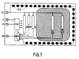
- Fig. 7 shows a digital integrated circuit comprising a circuit in accordance with the invention.
- the digital IC comprises connections for the supply of a control or input signal CS, a clock signal CK, a test data input TDI and a test data output TDO.
- the circuit also comprises a register of bistable elements BIST and a scan register SCAN, connected to combinatory logic (hatched area), and Boundary Scan cells BSC, further registers INST, BYP and ID, a multiplexer MUX, and also a finite state machine circuit FSM in accordance with the invention.
- Boundary Scan Test reference is made to Offenlegungsschrift DE-3727723-A1.
- the FSM determines state transitions in the registers.
- the testability of such ICs, constructed in Surface Mounting Technology, is of essential importance.
- the finite state machine circuit can be fully simulated. In an integrated circuit this can be realised using only little additional chip surface area.
Landscapes
- Physics & Mathematics (AREA)
- General Physics & Mathematics (AREA)
- Engineering & Computer Science (AREA)
- Automation & Control Theory (AREA)
- Logic Circuits (AREA)
- Test And Diagnosis Of Digital Computers (AREA)
- Tests Of Electronic Circuits (AREA)
Claims (6)
- Sequentielle Schaltung einer finiten Zustandsmaschine mit einer Menge N bistabiler Elemente {FF(1),...,FF(N)} und einer damit verbundenen Menge kombinatorischer Logik, wobei die Kombination von Logikwerten der bistabilen Elemente einen Zustand der Schaltung definiert, der eine Darstellung eines Zustandes einer finiten Zustandsmaschine ist, wobei die Schaltung zu von einem Taktsignal bestimmten Zeitpunkten, unter Einfluß der kombinatorischen Logik, des aktuellen Zustandes der Schaltung, und eines Eingangssignals, in einen nächsten Zustand übergeht, wobei die Menge kombinatorischer Logik Übergänge zwischen Zuständen der finiten Zustandsmaschine in der Schaltung realisiert, dadurch gekennzeichnet, daß von jedem Zustand aus mittels einer gegebenen Folge von X Werten des Eingangssignals, {c(0), c(1), ..., c(X-1)}, beginnend mit c(0), ein Ruhezustand erreicht wird, wobei jede Teilfolge {c(0), c(1), ... , c(J-1)}, mit der Länge J, die in der gegebenen Folge von X Werten des Eingangssignals auftritt, mit 1 ≦ J ≦ X, oder eine Teilfolge mit der Länge J, die eine Eins-zu-Eins-Darstellung davon ist, in der Schaltung gespeichert wird.
- Sequentielle Schaltung einer finiten Zustandsmaschine nach Anspruch 1, dadurch gekennzeichnet, daß die N bistabilen Elemente voreinstellbar sind, wobei die Schaltung mit (X-1) weiteren bistabilen Elementen versehen ist, als Schieberegister geschaltet, zur Speicherung der (X-1) neuesten Werte des Eingangssignals oder von Werten, die eine Eins-zu-Eins-Darstellung davon sind, und auch mit Decodierlogik versehen ist, der das Eingangssignal und die (X-1) bistabilen Elemente des Schieberegisters zugeführt werden, wobei diese Logik hinsichtlich des Auftretens der gegebenen Folge von X Werten des Eingangssignals ein Detektionssignal bildet und dieses Detektionssignal als Voreinstellsignal den N voreinstellbaren bistabilen Elementen zugeführt wird.
- Sequentielle Schaltung einer finiten Zustandsmaschine nach Anspruch 1, mit X ≧ N, dadurch gekennzeichnet, daß die Schaltung (X-N) weitere bistabile Elemente FF(N+1), ..., FF(X) umfaßt, und zusätzliche kombinatorische Logik, die, in Reaktion auf das Auftreten der Teilfolge {c(0), c(1), ..., c(J-1)}, mit der Länge J, der gegebenen Folge von X Werten des Eingangssignals, mit 1 ≦ J ≦ X, jedesmal die ersten J bistabilen Elemente FF(1), ..., FF(J) eine Darstellungsfolge von J Werten annehmen läßt, die eine Eins-zu-Eins-Darstellung der genannten Teilfolge ist, wobei die Zuweisung von Darstellungen an Zustände der finiten Zustandsmaschine derart ist, daß die Zustände durch Kombinationen von Logikwerten der bistabilen Elemente dargestellt werden, die hinsichtlich der ersten J Werte den Darstellungsfolgen von J Werten entsprechen.
- Sequentielle Schaltung einer finiten Zustandsmaschine nach Anspruch 1, mit X > = N, dadurch gekennzeichnet, daß die Schaltung (X-N) weitere bistabile Elemente zur Speicherung der (X-N) neuesten Werte des Eingangssignals, oder Werten, die eine Eins-zu-Eins-Darstellung davon sind, umfaßt, wobei die Schaltung auch zusätzliche Logik umfaßt, die, in Reaktion auf das Auftreten einer Teilfolge {c(0), c(1),..., c(J-1)}, mit der Länge J, der gegebenen Folge von X Werten des Eingangssignals, mit X-N < J ≦ X, jedesmal die ersten J-X+N bistabilen Elemente FF(1), ..., FF(J-X+N) eine Darstellungsfolge von J-X+N Werten annehmen läßt, die eine Eins-zu-Eins-Darstellung der genannten Teilfolge ist, wobei die Zuweisung von Darstellungen an Zustände der finiten Zustandsmaschine derart ist, daß die Zustände durch Kombinationen von Logikwerten der bistabilen Elemente dargestellt werden, die hinsichtlich der ersten J-X+N Werte den Darstellungsfolgen von J-X+N Werten entsprechen.
- Sequentielle Schaltung einer finiten Zustandsmaschine nach Anspruch 1, mit X < N, dadurch gekennzeichnet, daß die Schaltung zusätzliche Logik umfaßt, die in Reaktion auf das Auftreten einer Teilfolge {c(0), c(1), ..., c(J-1)}, mit der Länge J, der gegebenen Folge von X Werten des Eingangssignals, mit 1 ≦ J ≦ X, jedesmal die ersten J bistabilen Elemente FF(1), ..., FF(J) eine Darstellungsfolge von J annehmen läßt, die eine Eins-zu-Eins-Darstellung der genannten Teilfolge ist, wobei die Zuweisung von Darstellungen an Zustände der finiten Zustandsmaschine derart ist, daß die Zustände durch Kombinationen von Logikwerten der bistabilen Elemente dargestellt werden, die hinsichtlich der ersten J Werte den Darstellungsfolgen von J Werten entsprechen, wobei die zusätzliche Logik in Reaktion auf das Auftreten der gesamten Folge von X Werten des Eingangssignals, die bistabilen Elemente FF(X+1), ..., FF(N) Werte annehmen läßt, die den Logikwerten des Ruhezustandes entsprechen.
- Integrierte Schaltung mit einer sequentiellen Schaltung einer finiten Zustandsmaschine nach einem der Ansprüche 1 bis 5.
Applications Claiming Priority (2)
| Application Number | Priority Date | Filing Date | Title |
|---|---|---|---|
| NL9000380 | 1990-02-16 | ||
| NL9000380A NL9000380A (nl) | 1990-02-16 | 1990-02-16 | Sequentiele finite state machine schakeling, alsmede geintegreerde schakeling voorzien van de schakeling. |
Publications (2)
| Publication Number | Publication Date |
|---|---|
| EP0442580A1 EP0442580A1 (de) | 1991-08-21 |
| EP0442580B1 true EP0442580B1 (de) | 1995-05-17 |
Family
ID=19856615
Family Applications (1)
| Application Number | Title | Priority Date | Filing Date |
|---|---|---|---|
| EP91200295A Expired - Lifetime EP0442580B1 (de) | 1990-02-16 | 1991-02-13 | Sequentielle Endlichautomatenschaltung sowie integrierte Schaltung mit einer derartigen Schaltung |
Country Status (5)
| Country | Link |
|---|---|
| US (1) | US5097151A (de) |
| EP (1) | EP0442580B1 (de) |
| JP (1) | JPH04215316A (de) |
| DE (1) | DE69109703T2 (de) |
| NL (1) | NL9000380A (de) |
Families Citing this family (14)
| Publication number | Priority date | Publication date | Assignee | Title |
|---|---|---|---|---|
| EP0591593A1 (de) * | 1992-10-09 | 1994-04-13 | International Business Machines Corporation | Verfahren und Anordnung zur Verwaltung von asynchronen Ereignissen in einem endlichen Automaten |
| JP3563750B2 (ja) * | 1992-10-16 | 2004-09-08 | テキサス インスツルメンツ インコーポレイテツド | アナログ回路のための走査に基づく試験 |
| US5649163A (en) * | 1992-10-29 | 1997-07-15 | Altera Corporation | Method of programming an asynchronous load storage device using a representation of a clear/preset storage device |
| EP0618530A1 (de) * | 1993-03-30 | 1994-10-05 | Koninklijke Philips Electronics N.V. | Endlicher Automat mit Vorrichtung zum Reduzieren von Rauscheffekten |
| US5515292A (en) * | 1993-09-29 | 1996-05-07 | Texas Instruments Incorporated | Circuit activity driven state assignment of FSMS implemented in CMOS for low power reliable operations |
| JPH0887462A (ja) | 1994-09-20 | 1996-04-02 | Fujitsu Ltd | ステートマシン及び通信制御方式 |
| US6074428A (en) * | 1994-10-19 | 2000-06-13 | Hewlett-Packard Company | Minimizing logic by resolving "don't care" output values in a finite state machine |
| JP2967749B2 (ja) * | 1997-03-07 | 1999-10-25 | 日本電気株式会社 | テスト容易化論理合成システム |
| US5949251A (en) * | 1997-08-01 | 1999-09-07 | Vlsi Technology, Inc. | Register-based programmable post-silicon system to patch and dynamically modify the behavior of synchronous state machines |
| US6292023B1 (en) | 1999-09-29 | 2001-09-18 | Agere Systems Guardian Corp. | Spike-triggered asynchronous finite state machine |
| US6892343B2 (en) | 2000-03-27 | 2005-05-10 | Board Of Regents Of The University Of Nebraska | System and method for joint source-channel encoding, with symbol decoding and error correction |
| JP2004336010A (ja) * | 2003-04-16 | 2004-11-25 | Seiko Epson Corp | 半導体集積回路、電子機器、及びトランジスタのバックゲート電位制御方法 |
| US7877401B1 (en) * | 2006-05-24 | 2011-01-25 | Tilera Corporation | Pattern matching |
| US10338558B2 (en) * | 2014-10-17 | 2019-07-02 | 21, Inc. | Sequential logic circuitry with reduced dynamic power consumption |
Family Cites Families (7)
| Publication number | Priority date | Publication date | Assignee | Title |
|---|---|---|---|---|
| US4488229A (en) * | 1982-12-08 | 1984-12-11 | At&T Bell Laboratories | PLA-Based finite state machine with two-level control timing and same-cycle decision-making capability |
| US4649498A (en) * | 1984-05-08 | 1987-03-10 | The University Of Rochester | Computer systems for curve-solid classification and solid modeling |
| US4663545A (en) * | 1984-11-15 | 1987-05-05 | Motorola, Inc. | High speed state machine |
| HU195344B (en) * | 1984-12-19 | 1988-04-28 | Telefongyar | Circuit arrangement for forming sequential control circuit |
| US4755967A (en) * | 1986-03-21 | 1988-07-05 | Monolithic Memories, Inc. | Programmable synchronous sequential state machine or sequencer having decision variable input mapping circuit responsive to feedback signals |
| US4675556A (en) * | 1986-06-09 | 1987-06-23 | Intel Corporation | Binomially-encoded finite state machine |
| NL192801C (nl) * | 1986-09-10 | 1998-02-03 | Philips Electronics Nv | Werkwijze voor het testen van een drager met meerdere digitaal-werkende geïntegreerde schakelingen, geïntegreerde schakeling geschikt voor het aanbrengen op een aldus te testen drager, en drager voorzien van meerdere van zulke geïntegreerde schakelingen. |
-
1990
- 1990-02-16 NL NL9000380A patent/NL9000380A/nl not_active Application Discontinuation
-
1991
- 1991-02-13 JP JP3040530A patent/JPH04215316A/ja active Pending
- 1991-02-13 US US07/657,005 patent/US5097151A/en not_active Expired - Fee Related
- 1991-02-13 DE DE69109703T patent/DE69109703T2/de not_active Expired - Fee Related
- 1991-02-13 EP EP91200295A patent/EP0442580B1/de not_active Expired - Lifetime
Also Published As
| Publication number | Publication date |
|---|---|
| NL9000380A (nl) | 1991-09-16 |
| DE69109703T2 (de) | 1996-01-25 |
| JPH04215316A (ja) | 1992-08-06 |
| US5097151A (en) | 1992-03-17 |
| DE69109703D1 (de) | 1995-06-22 |
| EP0442580A1 (de) | 1991-08-21 |
Similar Documents
| Publication | Publication Date | Title |
|---|---|---|
| EP0442580B1 (de) | Sequentielle Endlichautomatenschaltung sowie integrierte Schaltung mit einer derartigen Schaltung | |
| EP0096176B1 (de) | Logische Simulationsverfahren und logisches Simulationsgerät | |
| US4313200A (en) | Logic test system permitting test pattern changes without dummy cycles | |
| JP3220480B2 (ja) | 自動テスト装置用イベントシーケンサ | |
| EP0978124B1 (de) | Verfahren zum überprüfen eines integrierten speichers mit hilfe einer integrierten dma-schaltung | |
| US4402081A (en) | Semiconductor memory test pattern generating apparatus | |
| US4365311A (en) | Control of instruction pipeline in data processing system | |
| JPS6134173B2 (de) | ||
| JPH10283381A (ja) | ゲーテッドクロック設計支援方法、ゲーテッドクロック設計支援装置及びゲーテッドクロック設計支援プログラムを格納したコンピュータ読み取り可能な記録媒体 | |
| EP0025087A2 (de) | Pipeline-Steuerung zur Erzeugung von Befehlen in einer digitalen Rechenanlage | |
| KR950007886B1 (ko) | 정보처리장치의 자기시험회로 | |
| US5331570A (en) | Method for generating test access procedures | |
| EP0204130B1 (de) | Gerät zur Verminderung des Bedarfs an Prüfdatenspeicher zur Prüfung von Hochgeschwindigkeits-VLSI-Schaltungen | |
| US4025768A (en) | Method and apparatus for testing and diagnosing data processing circuitry | |
| US6237117B1 (en) | Method for testing circuit design using exhaustive test vector sequence | |
| EP0699999A2 (de) | Speicherarchitektur für eine automatische Testeinrichtung mit Vektormodultabelle | |
| US4556976A (en) | Checking sequential logic circuits | |
| Chappell et al. | Simulation of large asynchronous logic circuits using an ambiguous gate model | |
| US6072948A (en) | Device for rapid simulation of logic circuits | |
| JPS59122972A (ja) | 論理回路試験装置 | |
| Marlett | On the design and testing of self-diagnosable computers. | |
| SU1524055A1 (ru) | Устройство дл контрол программ | |
| JPH04244979A (ja) | 遅延テストパターン及びその作成方法 | |
| EP0397532A2 (de) | Simulationssystem | |
| JPS6250860B2 (de) |
Legal Events
| Date | Code | Title | Description |
|---|---|---|---|
| PUAI | Public reference made under article 153(3) epc to a published international application that has entered the european phase |
Free format text: ORIGINAL CODE: 0009012 |
|
| AK | Designated contracting states |
Kind code of ref document: A1 Designated state(s): DE FR GB |
|
| 17P | Request for examination filed |
Effective date: 19920221 |
|
| 17Q | First examination report despatched |
Effective date: 19940606 |
|
| GRAA | (expected) grant |
Free format text: ORIGINAL CODE: 0009210 |
|
| AK | Designated contracting states |
Kind code of ref document: B1 Designated state(s): DE FR GB |
|
| REF | Corresponds to: |
Ref document number: 69109703 Country of ref document: DE Date of ref document: 19950622 |
|
| ET | Fr: translation filed | ||
| PLBE | No opposition filed within time limit |
Free format text: ORIGINAL CODE: 0009261 |
|
| STAA | Information on the status of an ep patent application or granted ep patent |
Free format text: STATUS: NO OPPOSITION FILED WITHIN TIME LIMIT |
|
| 26N | No opposition filed | ||
| REG | Reference to a national code |
Ref country code: FR Ref legal event code: CD |
|
| REG | Reference to a national code |
Ref country code: GB Ref legal event code: IF02 |
|
| PGFP | Annual fee paid to national office [announced via postgrant information from national office to epo] |
Ref country code: FR Payment date: 20020222 Year of fee payment: 12 |
|
| PGFP | Annual fee paid to national office [announced via postgrant information from national office to epo] |
Ref country code: GB Payment date: 20020228 Year of fee payment: 12 |
|
| PGFP | Annual fee paid to national office [announced via postgrant information from national office to epo] |
Ref country code: DE Payment date: 20020417 Year of fee payment: 12 |
|
| PG25 | Lapsed in a contracting state [announced via postgrant information from national office to epo] |
Ref country code: GB Free format text: LAPSE BECAUSE OF NON-PAYMENT OF DUE FEES Effective date: 20030213 |
|
| PG25 | Lapsed in a contracting state [announced via postgrant information from national office to epo] |
Ref country code: DE Free format text: LAPSE BECAUSE OF NON-PAYMENT OF DUE FEES Effective date: 20030902 |
|
| GBPC | Gb: european patent ceased through non-payment of renewal fee | ||
| PG25 | Lapsed in a contracting state [announced via postgrant information from national office to epo] |
Ref country code: FR Free format text: LAPSE BECAUSE OF NON-PAYMENT OF DUE FEES Effective date: 20031031 |
|
| REG | Reference to a national code |
Ref country code: FR Ref legal event code: ST |